 | –≠–ª–µ–∫—Ç—Ä–æ–Ω–Ω—ã–π –∫–æ–º–ø–æ–Ω–µ–Ω—Ç: DP83220 | –°–∫–∞—á–∞—Ç—å:  PDF PDF  ZIP ZIP |
TL F 11724
DP83220
CDL
Twisted
Pair
FDDI
Transceiver
Device
ADVANCE INFORMATION
October 1992
DP83220
CDL
TM
Twisted Pair FDDI Transceiver Device
General Description
The Copper Data Link (CDL) Transceiver is an integrated
circuit designed to interface directly with the National Semi-
conductor FDDI Chip Set or other FDDI PHY silicon allow-
ing low cost FDDI compatible data links over copper based
media The DP83220 Transceiver with the proper compen-
sation selected will allow links of up to 100 meters over
both Shielded Twisted Pair (STP) and Datagrade unshielded
Twisted Pair (DTP) CDL surpasses a Bit Error Rate (BER)
of
k
1
c
10
b
12
over both STP and DTP The CDL is de-
signed to meet the SDDI specification for FDDI transmission
across Type 1 STP cable when used in conjunction with the
appropriate transformer filter module from Pulse Engineer-
ing
Features
Y
Fully compatible with current FDDI PHY standard
Y
Fully compatible with the SDDI PMD specification
Y
Requires a single
a
5V supply
Y
Isolated TX and RX power supplies for minimum noise
coupling
Y
Allows use of Type 1 STP and Category 5 DTP cables
Y
No Transmit Clock required
Y
Loopback feature for board diagnostics
Y
Link Detect input provided
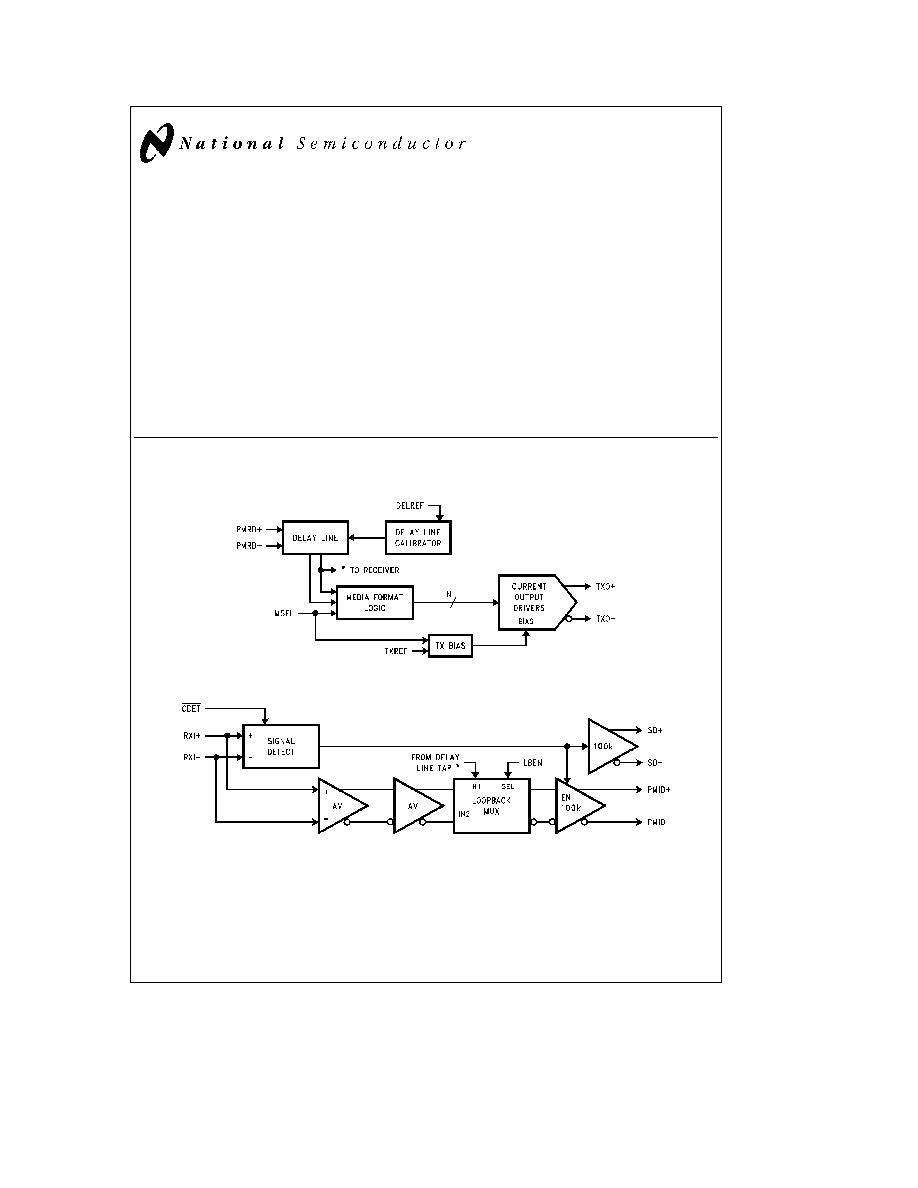
Block Diagram
Transmit Section
TL F 11724 ≠ 1
Receive Section
TL F 11724 ≠ 2
FIGURE 1 DP83220 Transceiver Block Diagram
CDL
TM
CDD
TM
CRD
TM
and PLAYER
TM
are trademarks of National Semiconductor Corporation
C1995 National Semiconductor Corporation
RRD-B30M105 Printed in U S A
1 0 Functional Description
The CDL Transceiver consists of nine major functional
blocks as shown in
Figure 1 The Transmit section includes
the following the Delay Line the Delay Line Calibrator the
Media Format Logic and the Current Output Driver circuitry
with its bias circuitry The Delay Line accepts the NRZI en-
coded data from the PMRD
g
pins and provides a short
``memory'' of the bit that preceded the bit currently being
transmitted The Delay Line Calibrator allows the use of an
external resistor which governs the time calibration of the
delay line The Delay Line outputs the data via taps which
are tied to the Media Format Logic The encoding logic is
dependent on the state of the Media Select pin The encod-
ed data is routed to the Current Output Driver through the
TXO
g
output pins and transformer coupled to the media
The Receive section consists of the following a differential
input amplifier Signal Detect circuitry a Loopback Multi-
plexer and differential 100K output drivers for data and Sig-
nal Detect The Receive signal is input to the RXI
g
pins
from the receive isolation transformer The input signal is
sensed by the Signal Detect circuit The input signal also
drives a differential input amplifier whose output is coupled
to the Loopback Mux logic The `sel' input which is driven by
LBEN controls which data stream RXI
g
or Loopback data
is routed to the differential 100K Output Driver When in
Loopback mode the Signal Detect output driver is forced
true When receiving data from copper media the signal
detect circuit provides valid states to the Signal Detect out-
put driver depending on the amplitude of the incoming sig-
nal and also allows the PMID
g
outputs to switch Cable
Detect is the final gating function for data reception If no
media is detected the transceiver will generate a logic low
Signal Detect which will inhibit data reception by the PHY
1 1 SDDI OPERATION
The CDL allows full compatibility with the current SDDI
specification By allowing the MSEL pin to float which
forces the pin to V
CC
2 internally the SDDI mode of opera-
tion is selected The appropriate transmit voltage amplitude
must also be set by selecting a value of 2 6 kX for the
TXREF resistor
Finally it is important to note that the CDL must be used in
conjunction with the Pulse Engineering 8 3 magnetics mod-
ule in order to conform to the current SDDI specification No
special terminations are required in connecting the Pulse
Engineering 8 3 module to the CDL (Refer to the typical
SDDI schematic
Figure 9 )
2 0 Pinout Summary
Signal
Pin No
Description
Type
V
CC
13 26
V
CC
Supply
GND
14 22
GND
Supply
RXV
CC
4 27
Receive V
CC
Supply
RXGND
3 28
Receive GND
Supply
TXV
CC
5 11
Transmit V
CC
Supply
TXGND
7 10
Transmit GND
Supply
EXTV
CC
23
External V
CC
Supply
RXI
g
2 1
Receive Data Inputs
Current In
PMID
g
25 24
Physical Media Indicate Data
ECL Out
PMRD
g
15 16
Physical Media Request Data
ECL In
TXO
g
9 8
Transmit Data Outputs
Current Out
SD
g
20 21
Signal Detect Outputs
ECL Out
TXREF
6
Transmit Amplitude Reference
Current Out
DELREF
12
Delay Line Calibration Reference
Current Out
LBEN
19
Loopback Enable
CMOS In
MSEL
17
Media Select
3-Level Select
CDET
18
Cable Detect Bar
CMOS Schmitt Trigger In
2

3 0 Pin Definitions
V
CC
(13 26)
Positive power supply for the 100K ECL com-
patible circuitry The Transceiver operates from a single
a
5 V
DC
power supply
GND (14 22)
Return path for the 100K ECL compatible cir-
cuitry power supply
RXV
CC
(4 27)
Positive power supply for the small signal
receive circuitry This power supply is intentionally separat-
ed from others to eliminate receive errors due to coupled
supply noise
RXGND (3 28)
Return path for the receive power supply
circuitry This Power supply return is intentionally separated
from others to eliminate receive errors due to coupled sup-
ply noise
TXV
CC
(5 11)
Positive power supply required by the analog
portion of the transmit circuitry This power supply is inten-
tionally separated from the others to prevent supply noise
from coupling to the transmit outputs
TXGND (7 10)
Return path for the analog transmit power
supply circuitry This supply return is intentionally separated
from others to prevent supply noise from being coupled to
the transmit outputs
EXTV
CC
(23)
Positive power supply for receiver output cir-
cuitry
RXI
g
(2 1)
Balanced differential line receiver inputs Sig-
nals meeting the input threshold for a given media type are
output through PMID
g
as differential ECL
PMID
g
(25 24)
100K ECL compatible differential outputs
used as the source of the receive data for the DP83231
Clock Recover Device (CRD
TM
)
PMRD
g
(15 16)
Differential 100K compatible 4B5B NRZI
transmit data inputs originating from the DP83251 55 Physi-
cal Layer Device (PLAYER
TM
)
TXO
g
(9 8)
Differential current driver outputs precompen-
sated for twisted pair cable
SD
g
(20 21)
Differential 100K ECL compatible Signal De-
tect outputs indicating that a valid signal is present at the
RXI
g
inputs
DELREF (12)
A resistor is connected between this pin and
GND The value of this resistor controls the current into the
delay line calibrator which in turn controls the delay time of
the delay line
TXREF (6)
A resistor is connected between this pin and
TXGND The value of this resistor controls the signal ampli-
tude of the TXO
g
data which drives the twisted pair
LBEN (19)
TTL compatible CMOS Loopback Enable input
pin selects the internal loopback path which effectively
routes the PMRD
g
data to the PMID
g
differential outputs
MSEL (17)
The Media Select input controls the compensa-
tion and output current required to drive to 100 meters of
either STP or DTP media This is a tri-Ievel control pin
When forced to a low voltage STP compensation is select-
ed Forcing a high voltage level will select the DTP compen-
sation mode Forcing a median voltage allows the device to
operate in the transparent mode by deasserting pre-empha-
sis
CDET (18)
The Cable Detect input is provided to support
the option of external Cable Detection circuitry With CDET
low the CDL transceiver functions normally When CDET is
high the signal detect output is forced low which inhibits
data reception by the PHY The exception is in the case of
Loop Back where Signal Detect is forced high regardless
28-Pin PLCC
TL F 11724 ≠ 3
Order Number DP83220V
See NS Package Number V28A
FIGURE 2 Pin Configuration
TL F 11724 ≠ 4
FIGURE 3 System Connection Diagram
3
4 0 Electrical Characteristics
ABSOLUTE MAXIMUM RATINGS
Symbol
Parameter
Conditions
Min
Typ
Max
Units
V
CC
Logic Power
Referenced to GND
b
0 5
6 0
V
RXV
CC
Received Power
Referenced to RXGND
b
0 5
6 0
V
TXV
CC
Transmit Power
Referenced to TXGND
b
0 5
6 0
V
EXTV
CC
ECL Output Power
Referenced to GND
b
0 5
6 0
V
I
ECL
DC Output Current (High)
b
50
mA
ESD
TBD
T
storage
Storage Temperature
b
65
a
150
C
4 1 RECOMMENDED OPERATING CONDITIONS
Symbol
Parameter
Conditions
Min
Typ
Max
Units
V
CC
Supply Voltage
4 5
5 0
5 5
V
T
A
Operating Temperature
0
25
70
C
P
D
Power Dissipation
600
mW
4 2 DC ELECTRICAL CHARACTERISTICS
T
A
e
25 C
Symbol
Parameter
Conditions
Min
Typ
Max
Units
V
IHt
TTL High Level Input
2 0
V
V
ILt
TTL Low Level Input
0 8
V
V
IHschmitt
Schmitt High Level Input
3 7
V
V
ILschmitt
Schmitt Low Level Input
1 5
V
V
IHmsel
MSEL High Level Input
3 7
V
V
ILmsel
MSEL Low Level Input
1 5
V
V
IMmsel
MSEL Middle Level Input
V
CC
2
V
V
IHe
ECL High Level Input
V
CC
b
1165
V
CC
b
870
mV
V
ILe
ECL Low Level Input
V
CC
b
1830
V
CC
b
1475
mV
V
OHe
ECL High Level Output
Refer to
Figure 4
V
CC
b
1035
V
CC
b
870
mV
V
OLe
ECL Low Level Output
Refer to
Figure 4
V
CC
b
1830
V
CC
b
1605
mV
I
CC1
Refer to
Figure 4
90
mA
I
CCT
Total Supply Current
Refer to
Figure 4
145
mA
I
TXO1
Transmit Current 1
Transmit Current
100X Z
O
20
mA
I
TXO2
Transmit Current 2
Transmit Current
150X Z
O
15
mA
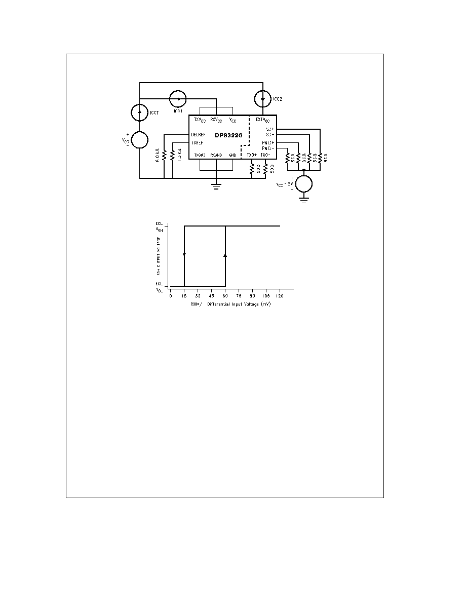
SD
THon
Sig Det Turn-On Threshold
Refer to
Figure 5 Note 1
60
mV
SD
THoff
Sig Det Turn-Off Threshold
Refer to
Figure 5 Note 1
15
mV
4 3 AC ELECTRICAL CHARACTERISTICS
T
A
e
25 C
Symbol
Parameter
Conditions
Min
Typ
Max
Units
t
TXr f
TX Driver Rise and Fall
Into 25X in Parallel with 50 pF
1 6
ns
t
TXr f
TX Driver Rise and Fall
Into 37 5X in Parallel with 50 pF
2 5
ns
t
TXpd
TX Propagation Delay
From PMRD
g
to TXO
g
6
ns
t
RXpd
RX Propagation Delay
From RXI
g
to PMID
g
10
ns
T
TXskew
TX Driver Skew
0
ps
Note 1
Subject to change
4
4 0 Electrical Characteristics
(Continued)
TL F 11724 ≠ 5
FIGURE 4 I
CC
Diagram
TL F 11724 ≠ 6
FIGURE 5 Signal Detect Threshold
5