DP83223
1
© 1997 National Semiconductor Corporation
General Description
The DP83223 Twisted Pair Transceiver is an integrated
circuit capable of driving and receiving three-level (MLT-3)
encoded datastreams. The DP83223 Transceiver is
designed to interface directly with National
Semiconductor's Fast Ethernet and FDDI Chip Sets or
similar Physical Layer silicon allowing low cost data links
over copper based media. The DP83223 allows links of up
to 100 meters over Shielded Twisted Pair (Type-1A STP)
and Category-5 datagrade Unshielded Twisted Pair (Cat-5
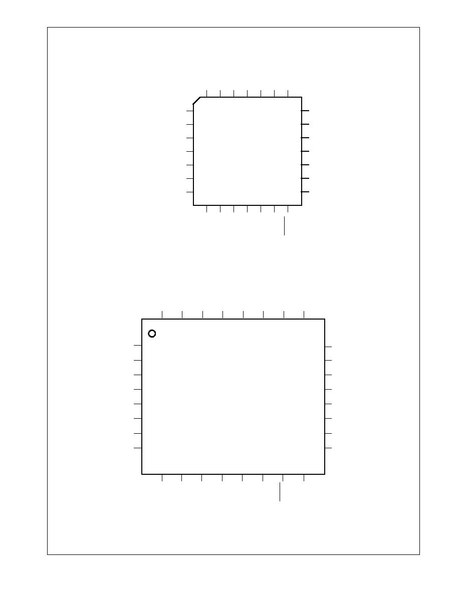
UTP) or equivalent. The DP83223 is available in a 28 pin
PLCC package and a 32 pin PQFP package.
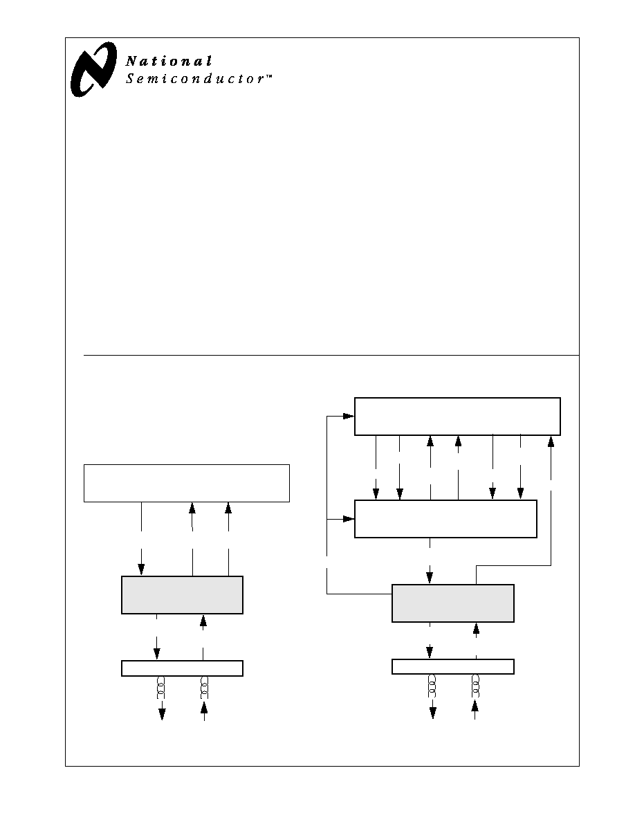
System Connection Diagrams
Features
s
Compatible with ANSI X3.263 TP-PMD draft standard
s
Allows use of Type 1 STP and Category 5 UTP cables
s
Requires a single +5V supply
s
Integrated transmitter and receiver with adaptive equal-
ization circuit
s
Isolated TX and RX power supplies for minimum noise
coupling
s
Loopback feature for board diagnostics
s
Digitally Synthesized transmit signal transition time con-
trol for reduced EMI
s
Programmable transmit voltage amplitude
s
Suitable for 100BASE-TX Fast Ethernet and Twisted
Pair FDDI applications
DP83223 TWISTER High Speed Networking Transceiver Device
April, 1997
DP83223
Transceiver
DP83840A
10/100 Ethernet PHY
Twisted Pair
Magnetics
Media
PMD
Encoded
RXDATA
PMD
Encoded
TXDATA
Scrambled
TX DATA
Signal
Scrambled
RX DATA
Detect
100BASE-TX
DP83257VF or DP83256VF-AP
PLAYER+
DP83223
Transceiver
Twisted Pair
Magnetics
DP83222
Stream Cipher
Media
TXC
SIGDET
Phased
RX CLOCK
Recovered
RXCLOCK
TX DATA
Scrambled
TX DATA
PMD
Encoded
RXDATA
PMD
Encoded
TXDATA
Descrambled
RX DATA
Recovered
RX DATA
RXDATA
Twisted Pair FDDI

4
DP83223
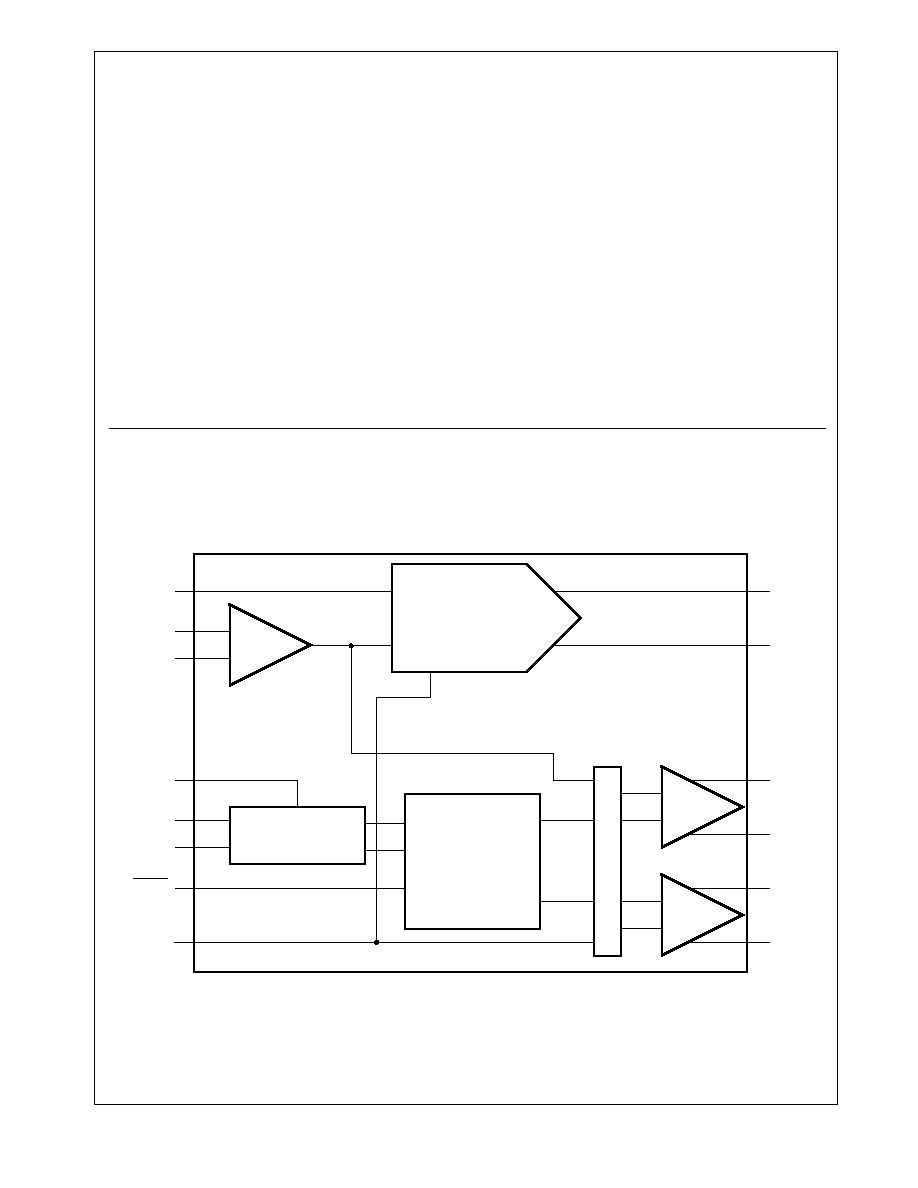
2.0 Pin Description
DP83223 Pinout Summary
Symbol
Pin No
PLCC(PQFP)
Type
Description
V
CC
13,26 (10, 25)
Supply
Vcc: Positive power supply for the ECL compatible circuitry. The
Transceiver operates from a single +5VDC power supply.
GND
14, 22(11 ,20)
Supply
GND: Return path for the ECL compatible circuitry power supply.
RXVcc
4, 27(26, 31)
Supply
Receive Vcc: Positive power supply for the small signal receive circuitry.
This power supply is intentionally separated from others to eliminate
receive errors due to coupled supply noise.
RXGND
3, 28(27, 30)
Supply
Receive GND: Return path for the receive power supply circuitry. This
power supply return is intentionally separated from others to eliminate
receive errors due to coupled supply noise.
TXVcc
5, 11(1, 7)
Supply
Transmit Vcc: Positive power supply required by the analog portion of the
transmit circuitry. This power supply is intentionally separated from the
others to prevent supply noise from coupling to the transmit outputs.
TXGND
7, 10(3, 6)
Supply
Transmit GND: Return path for the analog transmit power supply circuitry.
This supply return is intentionally separated from others to prevent supply
noise from being coupled to the transmit outputs.
EXTVcc
23(21)
Supply
External Vcc: Positive power supply for ECL output circuitry.
RXI+/-
2, 1(29, 28)
Differential
Voltage In
Receive Data Inputs: Balanced differential line receiver inputs.
PMID+/-
25, 24(23, 22)
ECL Out
Physical Media Indicate Data: Differential ECL compatible outputs
source the recovered receive data back to the Physical Layer device or to
a separate clock recovery device.
PMRD+/-
15, 16(12,13)
ECL In
Physical Media Request Data: Differential ECL compatible inputs which
receive data from Physical Layer Device.
TXO+/-
9, 8(5,4)
Differential
Current
Out
Transmit Data Outputs: Differential current driver outputs which drive
MLT-3 encoded data over twisted pair cable. These outputs provide
controlled rise and fall times designed to filter the transmitters output which
helps to reduce associated EMI.
SD+/-
20, 21(18, 19)
ECL Out
Signal Detect Outputs: Differential ECL compatible Signal Detect outputs
indicating that either a signal with the proper amplitude is present at the
RXI+/- inputs or that Loopback mode has been selected.
TXREF
6(2)
Current
Out
Transmit Amplitude Reference:
Reference current pin allowing
adjustment of TXO+/- transmit amplitude. By placing a resistor between
this pin and GND, a reference current is setup which results in a given
transmit amplitude for a given application. Refer to Functional Description
in Section 3.1 for reference current equations.
ENCSEL
12(9)
CMOS In Encode Select Input: The TTL compatible CMOS Encode Select input
controls the encoded state of the signal at the TXO+/- outputs. A logic low
level at this input causes the TXO outputs to become MLT-3 encoded with
the receiver programmed to accept MLT-3 encoded data. This is the
recommended mode of operation. A logic high level causes the TXO pins
to output standard two-level binary code and the receiver is conditioned to
receive a two-level binary signal. The DP83223V does not guarantee this
mode(binary) of operation.
LBEN
19(17)
CMOS In Loopback Enable: TTL compatible CMOS Loopback Enable input pin
selects the internal loopback path which routes the PMRD+/- data to the
PMID+/- differential outputs and forces Signal Detect true. During
loopback, data present at the RXI+/- inputs is ignored. However, binary
data is still transmitted by the TXO+/- outputs (regardless of the state of the
ENCSEL input). Loopback mode is selected when LBEN is forced high.
Normal operation occurs when LBEN is forced low.
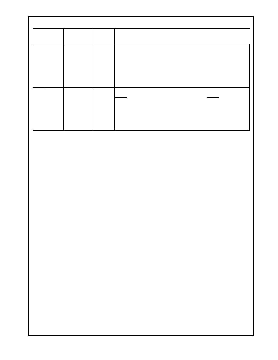
2.0 Pin Description
(Continued)
5
Revision A
DP83223
EQSEL
17(14)
3-Level Se-
lect
Equalization Select: This three level Equalization Select input controls the
mode of receiver equalization. Forcing a median voltage level,
accomplished by allowing EQSEL to float, selects the adaptive
equalization mode which automatically regulates the equalization effects
based on signal degradation caused by the media. The other two levels are
intended as test modes and are not a guaranteed mode of operation.
Forcing a voltage less than 1.5V, selects full equalization which provides
fixed equalization for a maximum length of cable. Forcing a voltage greater
than 3.0V turns the receive equalizer off.
CDET
18(15)
CMOS In Cable Detect Bar: The active low Cable Detect CMOS input is provided to
support the option of external Cable Detection circuitry (wire fault). With
CDET low, the transceiver functions normally. With CDET high, the signal
detect output is forced low which inhibits data reception by the PHY and
the PMID outputs are forced to ECL static levels. The exception is in the
case of Loopback when the Signal Detect output is forced high regardless
of all other conditions. Please refer to the National Semiconductor Com-
mon Magnetics application note for further detail regarding the proper use
of the DP83223 in a 10/100 Ethernet application.
Symbol
Pin No
PLCC(PQFP)
Type
Description