 | –≠–ª–µ–∫—Ç—Ä–æ–Ω–Ω—ã–π –∫–æ–º–ø–æ–Ω–µ–Ω—Ç: DP83261 | –°–∫–∞—á–∞—Ç—å:  PDF PDF  ZIP ZIP |
TL F 10387
DP83261
BMAC
Device
(FDDI
Media
Access
Controller)
October 1994
DP83261 BMAC
TM
Device
(FDDI Media Access Controller)
General Description
The DP83261 BMAC device implements the Media Access
Control (MAC) protocol for operation in an FDDI token ring
The BMAC device provides a flexible interface to the
BSI-2
TM
device The BMAC device offers the capabilities
described in the ANSI X3T9 5 MAC Standard and several
functional enhancements allowed by the Standard
The BMAC device transmits receives repeats and strips
tokens and frames It uses a full duplex architecture that
allows diagnostic transmission and self testing for error iso-
lation The duplex architecture also allows full duplex data
service on point-to-point connections Management soft-
ware is also aided by an array of on chip statistical counters
and the ability to internally generate Claim and Beacon
frames without program intervention A multi-frame stream-
ing interface is provided to the system interface device
Features
Y
Full duplex operation with through parity
Y
Supports all FDDI ring scheduling classes (asynchro-
nous synchronous restricted asynchronous and
immediate)
Y
Supports individual group short long and external
addressing
Y
Generates Beacon Claim and Void frames without
intervention
Y
Provides extensive ring and station statistics
Y
Provides extensions for MAC level bridging
Y
Provides separate management interface
Y
Uses low power microCMOS
TL F 10387 ≠ 1
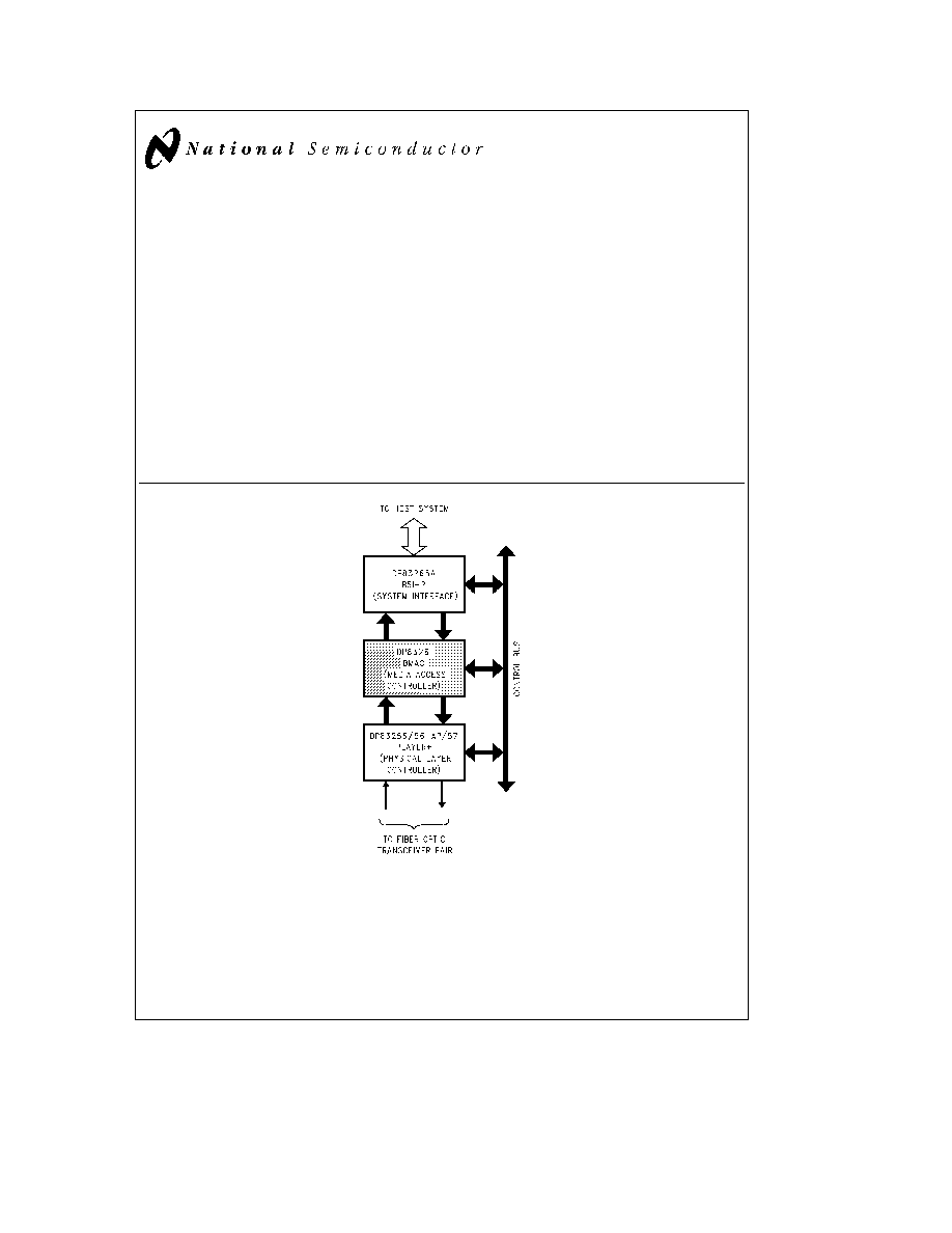
FIGURE 1-1 FDDI Chip Set Block Diagram
TRI-STATE is a registered trademark of National Semiconductor Corporation
BSI-2
TM
BMAC
TM
PLAYERa
TM
CDD
TM
and CRD
TM
are trademarks of National Semiconductor Corporation
C1995 National Semiconductor Corporation
RRD-B30M105 Printed in U S A

Table of Contents
1 0 FDDI CHIP SET OVERVIEW
2 0 ARCHITECTURAL DESCRIPTION
2 1 Ring Engine
2 2 Interfaces
3 0 FEATURE OVERVIEW
4 0 FDDI MAC FACILITIES
4 1 Symbol Set
4 2 Protocol Data Units
4 3 Frame Counts
4 4 Timers
4 5 Ring Scheduling
5 0 FUNCTIONAL DESCRIPTION
5 1 Token Handling
5 2 Servicing Transmission Requests
5 3 Request Service Parameters
5 4 Frame Validity Processing
5 5 Frame Status Processing
5 6 SMT Frame Processing
5 7 MAC Frame Processing
5 8 Receive Batching Support
5 9 Immediate Frame Transmission
5 10 Full Duplex Operation
5 11 Parity Processing
6 0 CONTROL INFORMATION
6 1 Conventions
6 2 Access Rules
6 3 Operation Registers
6 4 Event Registers
6 5 MAC Parameters
6 6 Timer Thresholds
6 7 Event Counters
7 0 SIGNAL DESCRIPTIONS
7 1 Control Interface
7 2 PHY Interface
7 3 MAC Indication Interface
7 4 MAC Request Interface
7 5 Electrical Interface
7 6 Pinout Summary
7 7 Pinout Diagram
8 0 ELECTRICAL CHARACTERISTICS
8 1 Absolute Maximum Ratings
8 2 Recommended Operating Conditions
8 3 DC Electrical Characteristics
8 4 AC Electrical Characteristics
APPENDIX A RING ENGINE STATE MACHINES
A 1 Receiver
A 2 Transmitter
2

1 0 FDDI Chip Set Overview
National Semiconductor's DP83200 FDDI chip set consists
of five components as shown in
Figure 1-1 For more infor-
mation on the other devices of the chip set consult the
appropriate datasheets and application notes
DP83256 56-AP 57 PLAYER
a
TM
Device Physical Layer Controller
The PLAYER
a
device implements the Physical Layer
(PHY) protocol as defined by the ANSI FDDI PHY X3T9 5
Standard along with all the necessary clock recovery and
clock regeneration functions
Features
Single chip FDDI Physical Layer (PHY) solution
Integrated Digital Clock Recovery Module provides en-
hanced tracking and greater lock acquisition range
Integrated Clock Generation Module provides all neces-
sary clock signals for an FDDI system from an external
12 5 MHz reference
Alternate PMD Interface (DP83256-AP 57) supports
UTP twisted pair FDDI PMDs with no external clock re-
covery or clock generation functions required
No External Filter Components
Connection Management (CMT) Support (LEM TNE
PC
React CF
React Auto Scrubbing)
Full on-chip configuration switch
Low Power CMOS-BIPOLAR design using a single 5V
supply
Full duplex operation with through parity
Separate management interface (Control Bus)
Selectable Parity on PHY-MAC Interface and Control Bus
Interface
Two levels of on-chip loopback
4B 5B encoder decoder
Framing logic
Elasticity Buffer Repeat Filter and Smoother
Line state detector generator
Supports single attach stations dual attach stations and
concentrators with no external logic
DP83256 56-AP for SAS DAS single path stations
P83257 for SAS DAS single dual path stations
In
addition
the
DP83257
contains
an
additional
PHY
Data request and PHY
Data indicate port required
for concentrators and dual attach stations
DP83261 BMAC
TM
Device
Media Access Controller
The BMAC device implements the Timed Token Media Ac-
cess Control protocol defined by the ANSI X3T9 5 FDDI
MAC Standard
Features
All of the standard defined ring service options
Full duplex operation with through parity
Supports all FDDI Ring Scheduling Classes (Synchro-
nous Asynchronous etc )
Supports Individual Group Short Long and External
Addressing
Generates Beacon Claim and Void frames internally
Extensive ring and station statistic gathering
Extensions for MAC level bridging
Separate management port that is used to configure and
control operation
Multi-frame streaming interface
DP83265A BSI-2 Device
System Interface
The BSI-2 device implements an interface between the
BMAC device and a host system
Features
Fully software and pin compatible with the original BSI
device
Over 2 kbytes of on-chip FIFO
Operates from 12 5 MHz to 33 MHz synchronously with
host system
Provides Address bit swapping capability
Reduces interface logic for SBus adapters
32-bit wide Address Data path with byte parity
Programmable transfer burst sizes of 4 or 8 32-bit words
Interfaces to DRAMs or directly to system bus
2 Output and 3 Input Channels
Supports Header Info splitting
Bridging support
Programmable Big or Little Endian alignment
Full duplex data path
Receive frame filtering services
3
2 0 Architectural Description
The BMAC device receivers transmits and strips or repeats
Protocol Data Units (PDUs i e
Tokens and Frames) and
handles the token management functions required by the
timed token protocol in accordance with the FDDI MAC
Standard
The BMAC device is comprised of the Ring Engine (RE) and
interfaces to the Control Bus (Control Interface)
the
PLAYER device (PHY Interface) and a System Interface
such as the BSI device (MAC Interface) as shown in
Figure 2-1
On transmission the system interface prepares one or more
frames for transmission and requests a service opportunity
Based on the requested service class and requested token
type the Ring Engine waits for a token meeting the request-
ed criteria When a token is captured the Ring Engine sig-
nals the interface and soon thereafter transmission begins
After traversing the ring frames are stripped based on the
Source Address Frames with a Source Address matching
one of the station individual addresses are stripped by the
Ring Engine Status is available at the MAC interface for
every transmitted frame
For reception the Ring Engine sequences through the in-
coming byte stream comparing received destination ad-
dresses against the station's short or long address The re-
sults of these comparisons are made available at the MAC
interface The System Interface then decides how to handle
the frame In the normal case a frame with a Destination
Address matching one of the station addresses is copied
and passed to the system
The BMAC device utilizes a full duplex byte-wide (symbol
pair) architecture There are two bytes of delay in the Trans-
mit path three bytes of delay in Receive and Repeat paths
and two bytes of delay in the Loopback path
TL F 10387 ≠ 2
FIGURE 2-1 BMAC Device Interfaces
4
2 0 Architectural Description
(Continued)
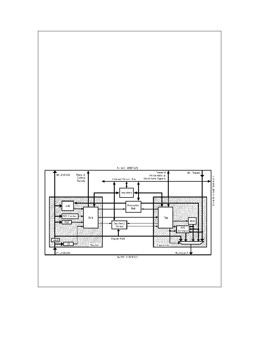
2 1 RING ENGINE
The BMAC device is operated by the Ring Engine which is
comprised of four blocks Receiver Transmitter MAC Pa-
rameter RAM and Counters Timers as shown in
Figure 2-2
2 1 1 Receiver
The Receiver Block accepts data from the PLAYER device
in the byte stream format (PH
Indicate)
Upon receiving the data the Receiver Block performs the
following functions
Determines the beginning and ending of a Protocol Data
Unit (PDU)
Decodes the Frame Control field to determine the PDU
type (frame or token)
Compares the received Destination and Source Address-
es with the internal addresses
Processes data within the frame
Calculates and checks the Frame Check Sequence at
the end of the frame
Checks the Frame Status field
And finally the Receiver Block presents the data to the
MAC Interface along with the appropriate control signals
(MA
Indicate)
2 1 2 Transmitter
The Transmitter Block inserts frames from this station into
the ring in accordance with the FDDI Timed Token MAC
protocol It also repeats frames from other stations in the
ring The Transmitter block multiplexes data from the MA
Request Interface and data from the Receiver Block During
Frame Transmission data from the Request Interface is se-
lected During Frame Repeating data from the Receiver
Block is selected
During Frame Transmission the Transmitter Block performs
the following functions
Captures a token to gain the right to transmit
Transmits one or more frames
Generates the Frame Check Sequence during transmis-
sion and appends it at the end of the frame
Generates the Frame Status field that is transmitted at
the end of the frame
Issues the token at the end of frame transmission
During Frame Repeating the Transmitter Block performs
the following functions
Repeats the received frame and modifies the Frame
Status field at the end of the frame as specified by the
standard
Whether transmitting or repeating frames the Transmitter
Block also performs the following functions
Strips the frame(s) that are transmitted by this station
Generates Idle symbols between frames
Data is presented from the Transmitter Block to the
PLAYER device in the byte stream format (PH
Request)
2 1 3 MAC Parameter RAM
The MAC Parameter RAM block is a dual port RAM that
contains MAC parameters such as the station's short and
long addresses These parameters are initiallzed via the
Control Interface Both the Receiver and Transmitter Blocks
may access the RAM
TL F 10387 ≠ 4
FIGURE 2-2 Ring Engine Overview Block Diagram
5