 | –≠–ª–µ–∫—Ç—Ä–æ–Ω–Ω—ã–π –∫–æ–º–ø–æ–Ω–µ–Ω—Ç: DP83291EB | –°–∫–∞—á–∞—Ç—å:  PDF PDF  ZIP ZIP |
TL F 10824
DP83291EB
FDDI
MAC
Layer
Evaluation
Board
April 1990
DP83291EB
FDDI MAC Layer Evaluation Board
General Description
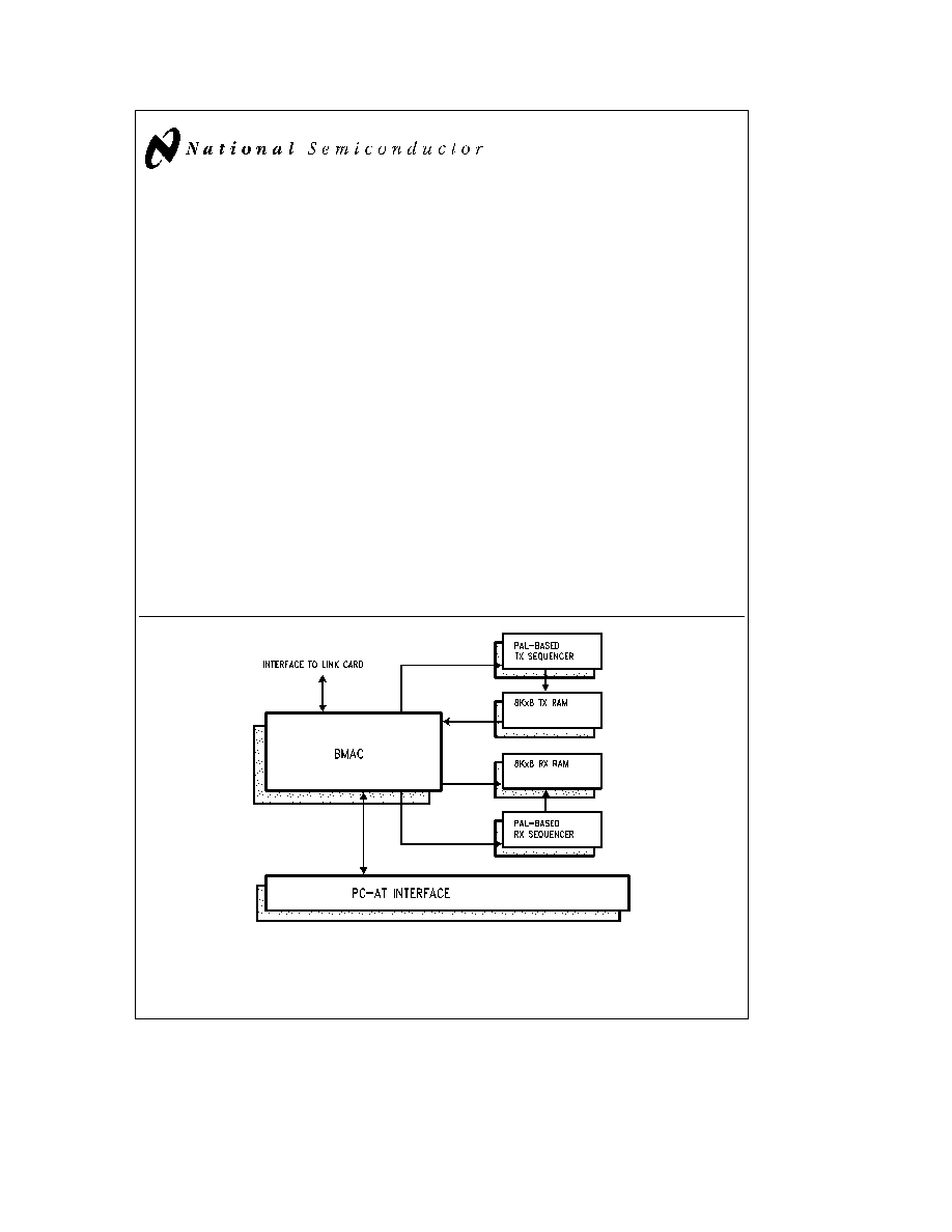
The DP83291EB FDDI MAC Layer Evaluation Board is a
PC-AT
compatible board that implements the MAC Layer
functions of the FDDI standard The Board utilizes the Na-
tional Semiconductor DP83261 BMAC
TM
device along with
PAL -based Buffer Management Logic to implement a sim-
ple MAC Layer
The MAC Demonstration Board features two 8k x 8 buffers
that are configured as Dual Ported Memory One memory
bank is dedicated to receive while the other is dedicated to
transmit This configuration supports full duplex transmis-
sion to self
The MAC board contains expansion connectors to interface
to the Link Card Three busses are provided two for data
paths and one for clock paths The MAC Card is used with a
single Link Card to implement a Single Attach Station (SAS)
and two Link Cards to implement a Dual Attach Station
(DAS)
Features
Y
PC-AT compatible full size card
Y
Dual ported memory interface
full duplex data path
Y
Interfaces to link cards for DAS or SAS configurations
Y
Supported by demonstration software
Y
Utilizes DP83261 BMAC device
Y
Full network statistics
Y
Supports asynchronous and synchronous transmission
classes
Y
Supports confirmation services
Y
PAL based buffer management
Table of Contents
1 0 General Description
2 0 Address Mapping
3 0 Installation
4 0 Board Register Description
5 0 Memory Interface
6 0 Frame Transmission
7 0 Frame Reception
8 0 Software Interface
9 0 Implementation Notes
Appendix
TL F 10824 ≠ 1
FIGURE 1 DP83291EB Block Diagram Overview
BMAC
TM
CDD
TM
and PLAYER
TM
are trademarks of National Semiconductor Corporation
PAL
is a registered trademark of and used under license from Advanced Micro Devices Inc
IBM PC
and PC-AT
are registered trademarks of International Business Machines Corporation
C1995 National Semiconductor Corporation
RRD-B30M105 Printed in U S A
1 0 General Description
The FDDI Evaluation Boards have been designed to dem-
onstrate the capabilities of National Semiconductor's FDDI
chip set
The Evaluation Board allows evaluation of the many capa-
bilities of the chip set and will serve as an educational tool
for customers designing products with the FDDI chip set
High performance as a goal was sacrificed at the expense
of simplicity and accessibility There are many laboratories
around the world with a spare IBM PC
or compatible
These boards allow users to experiment and gain experi-
ence with the FDDI chip set in order to unleash its capabili-
ties in their own products
1 1 BLOCK DIAGRAM
A simplified Block Diagram is shown in
Figure 2
1 2 OVERVIEW
The MAC Evaluation Board is designed to perform simple
transmission and reception scenarios One 8K by 8 Static
RAM is used for Transmission and another is used for Re-
ception and Status
On Transmission the Transmission Counter is used to ad-
dress the Tx
RAM where the frames to be transmitted are
written The Transmit Sequencer controls the sequencing of
frames across the BMAC device's MAC Request Interface
On Reception the Receive Sequencer controls the se-
quencing of frames across the BMAC device's MAC Indi-
cate Interface Transmit and Receive Status is stored and
multiplexed into the Rx
RAM between frames The Re-
ceive Counter is used to address the Rx
RAM The Re-
ceive Counter is under the control of the Receive Sequenc-
er The Copy PAL monitors the addressing information from
the BMAC device and determines whether to continue to
copy frames This is signaled to the Receive Sequencer
which then adjusts the Receive Counter accordingly
TL F 10824 ≠ 2
FIGURE 2 DP83291EB Block Diagram
2

1 0 General Description
(Continued)
The Tx
RAM contains either one maximum size frame or
up to 16 frames of 512 bytes or less The Rx
RAM may be
filled with up to 8 frames
The DP8570A is used as a timer on this board and provides
support for Station Management Its registers are accessed
via the PC interface and is memory mapped
The PC interface provides access to the Transmit and Re-
ceive RAM in addition to the Board Registers and BMAC
device The Board Registers include a Mode Function and
Status Register
2 0 Address Mapping
2 1 PC BUS INTERFACE
2 1 1 Board Address Mapping
The Evaluation Board Control Bus is mapped into a 64K
segment within the lowest 1M of the PC address space The
64K offset is selected (by a jumper) as shown below
Sel
e
0
offset is C0000
Sel
e
1
offset is D0000
2 1 2 64K Segment Mapping
The 64K segment reserved for the evaluation board is divid-
ed as shown below
0000
b
3FFF
used for control registers (See
Figure 3 )
4000
b
7FFF
reserved
8000
b
9FFF
used to access 8K Tx
RAM
A000
b
BFFF
shadow of Tx
RAM
C000
b
DFFF
used to access 8K Rx
RAM
E000
b
FFFF
shadow of Rx
RAM
2 1 3 Board Register Address Mapping
The address space used for control registers is divided into
512 byte pages for each PHY or MAC The MAC is select-
able as either MAC 0 or MAC 1
0000 ≠ 01FF MAC0
0200 ≠ 03FF MAC1
0400 ≠ 0FFF used for PHYs
1000 ≠ 3FFF reserved for future use
See
Figure 3
2 1 4 MAC Registers
0000 ≠ 00FF BMAC Device Registers
0100 ≠ 01FF Board Registers
2 1 4 1 BMAC Device Registers
The BMAC Device Registers are mapped directly into the
64K segment of the address space as defined in the BMAC
Device Datasheet
2 1 4 2 MAC Evaluation Board Registers
The board registers are mapped into the 64K segment of
the address space as
0100
Mode Register
0140
Function Register
0180
Status Register
01A0
Timer Registers
01C0
Board Reset
Note
For MAC1 add 200h to each address
BMAC 0 REGISTERS
0000-00FF
BOARD 0 REGISTERS
00FF-01FF
BMAC 1 REGISTERS
0200-02FF
BOARD 1 REGISTERS
0300-03FF
FUTURE PHYS
0400-0FFF
RESERVED
1000-3FFF
RESERVED
4000-7FFF
TX RAM
8000-9FFF
SHADOW TX RAM
A000-BFFF
RX RAM
C000-DFFF
SHADOW RX RAM
E000-FFFF
FIGURE 3 Board Address Map
3
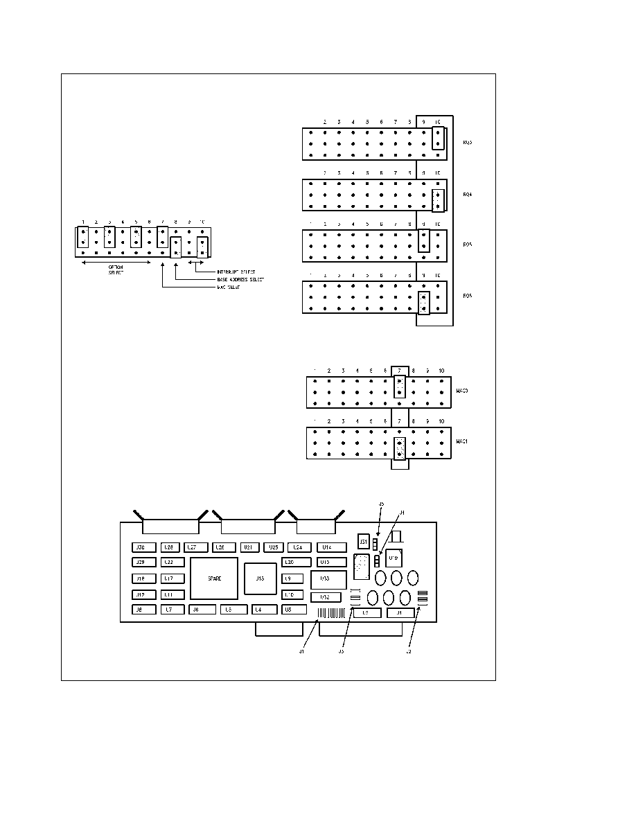
3 0 Board Installation
The MAC Card requires a full length slot It can be installed
in either an AT or XT slot There are several options that
can be programmed via jumpers provided on the MAC Card
The position of the jumpers on the board are shown in
Fig-
ure 4
3 1 JUMPER SETTINGS
3 1 1 J1 Base Address MAC Select Interrupt and
Option Selection
J1 is used to select the Base Address of the MAC Card
MAC Number interrupt to be used for the interconnected
MAC and Link Cards and Option Selections on the BMAC
device The possible settings and factory defaults follow
TL F 10824 ≠ 3
Factory Default Shown
3 1 2 Interrupts
TL F 10824 ≠ 4
Factory Default
e
IRQ4
3 1 3 MAC Select
TL F 10824 ≠ 5
Factory Default
e
MAC0
TL F 10824 ≠ 6
FIGURE 4 MAC Card Jumper Locations
4
3 0 Board Installation
(Continued)
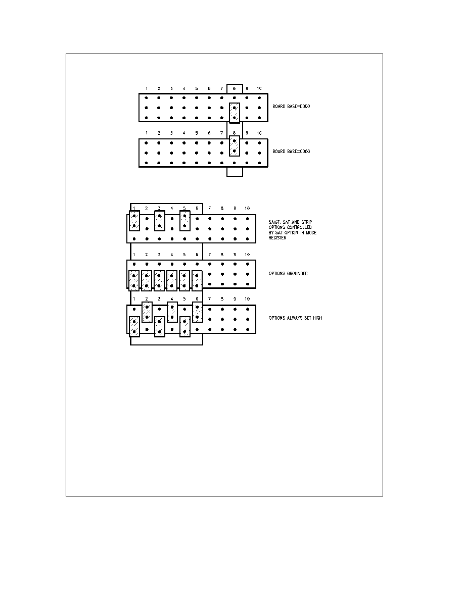
3 1 4 Base Address Select
TL F 10824 ≠ 7
Factory Default
e
D000
3 1 5 Options Selection
TL F 10824 ≠ 8
Factory Default
e
Options Controlled by SAT Option in Board Mode Register
5