1
National Semiconductor
Version A
March 1997
DP83840A 10/100 Mb/s Ethernet Physical Layer
General Description
The DP83840A is a Physical Layer device for Ethernet
10BASE-T and 100BASE-X using category 5 Unshielded,
Type 1 Shielded and Fiber Optic cables.
This VLSI device is designed for easy implementation of
10/100 Mb/s Ethernet LANs. It interfaces to the PMD sub-
layer through National Semiconductor's DP83223 Twisted
Pair Transceiver, and to the MAC layer through a Media
Independent Interface (MII), ensuring interoperability
between products from different vendors.
The DP83840A is designed with National Semiconductor's
BiCMOS process. Its system architecture is based on the
integration of several of National Semiconductor's industry
proven core technologies:
10BASE-T ENDEC/Transceiver module to provide the 10
Mb/s IEEE 802.3 functions
Clock Recovery/Generator Modules from National
Semiconductor's leading FDDI product
FDDI Stream Cipher (Cyclone)
100BASE-X physical coding sub-layer (PCS) and control
logic that integrate the core modules into a dual speed
Ethernet physical layer controller
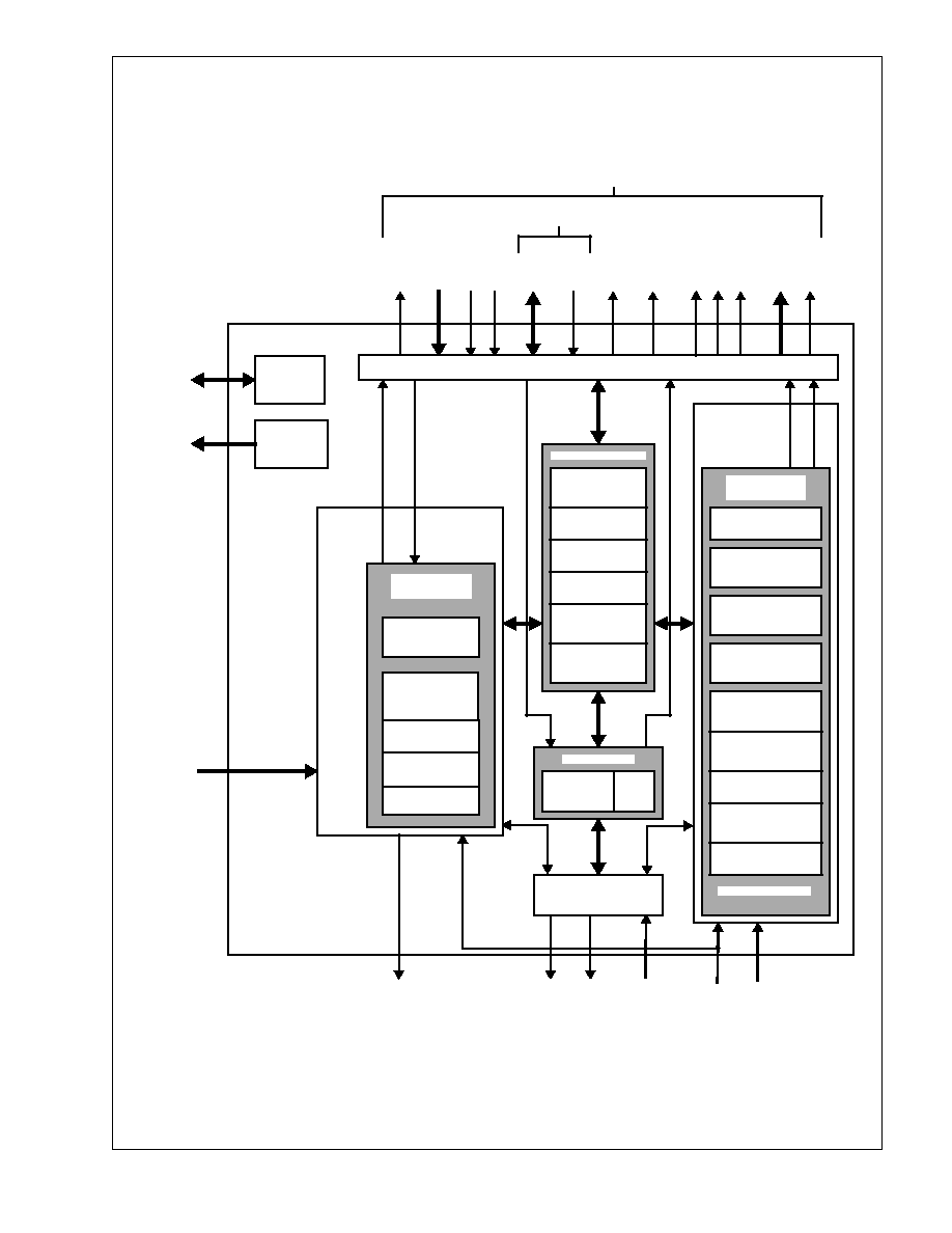
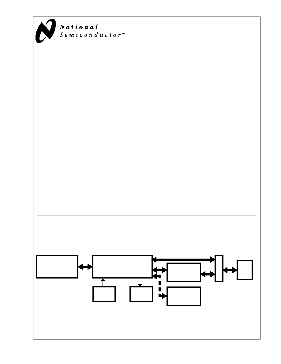
System Diagram
Features
∑
IEEE 802.3 10BASE-T compatible--ENDEC and UTP/
STP transceivers and filters built-in
∑
IEEE 802.3u 100BASE-X compatible--support for 2 pair
Category 5 UTP (100m), Type 1 STP and Fiber Optic
Transceivers--Connects directly to the DP83223 Twisted
Pair Transceiver
∑
ANSI X3T12 TP-PMD compatible
∑
IEEE 802.3u Auto-Negotiation for automatic speed
selection
∑
IEEE 802.3u compatible Media Independent Interface
(MII) with Serial Management Interface
∑
Integrated high performance 100 Mb/s clock recovery
circuitry requiring no external filters
∑
Full Duplex support for 10 and 100 Mb/s
∑
MII Serial 10 Mb/s output mode
∑
Fully configurable node and repeater modes--allows
operation in either application
∑
Programmable loopback modes for easy system
diagnostics
∑
Flexible LED support
∑
IEEE 1149.1 Standard Test Access Port and Boundary-
Scan compatible
∑
Small footprint 100-pin PQFP package
∑
Individualized scrambler seed for multi-PHY applications
DP83840A
10/100 Mb/s Ethernet Physical Layer
10 AND/OR 100 Mb/s
ETHERNET MAC OR
REPEATER/SWITCH
PORT
DP83840A
10/100 Mb/s
ETHERNET PHYSICAL LAYER
CLOCKS
STATUS
LEDS
DP83223
100BASE-TX
TRANSCEIVER
MA
GNETICS
RJ-45
10BASE-T
OR
100BASE-TX
MII
10BASE-T
100BASE-FX
TRANSCEIVER

3
Table of Contents
National Semiconductor
Version A
DP83840A 10/100 Mb/s Ethernet Physical Layer
GENERAL DESCRIPTION
FEATURES
SYSTEM DIAGRAM
BLOCK DIAGRAM
REVISION HISTORY
TABLE OF CONTENTS
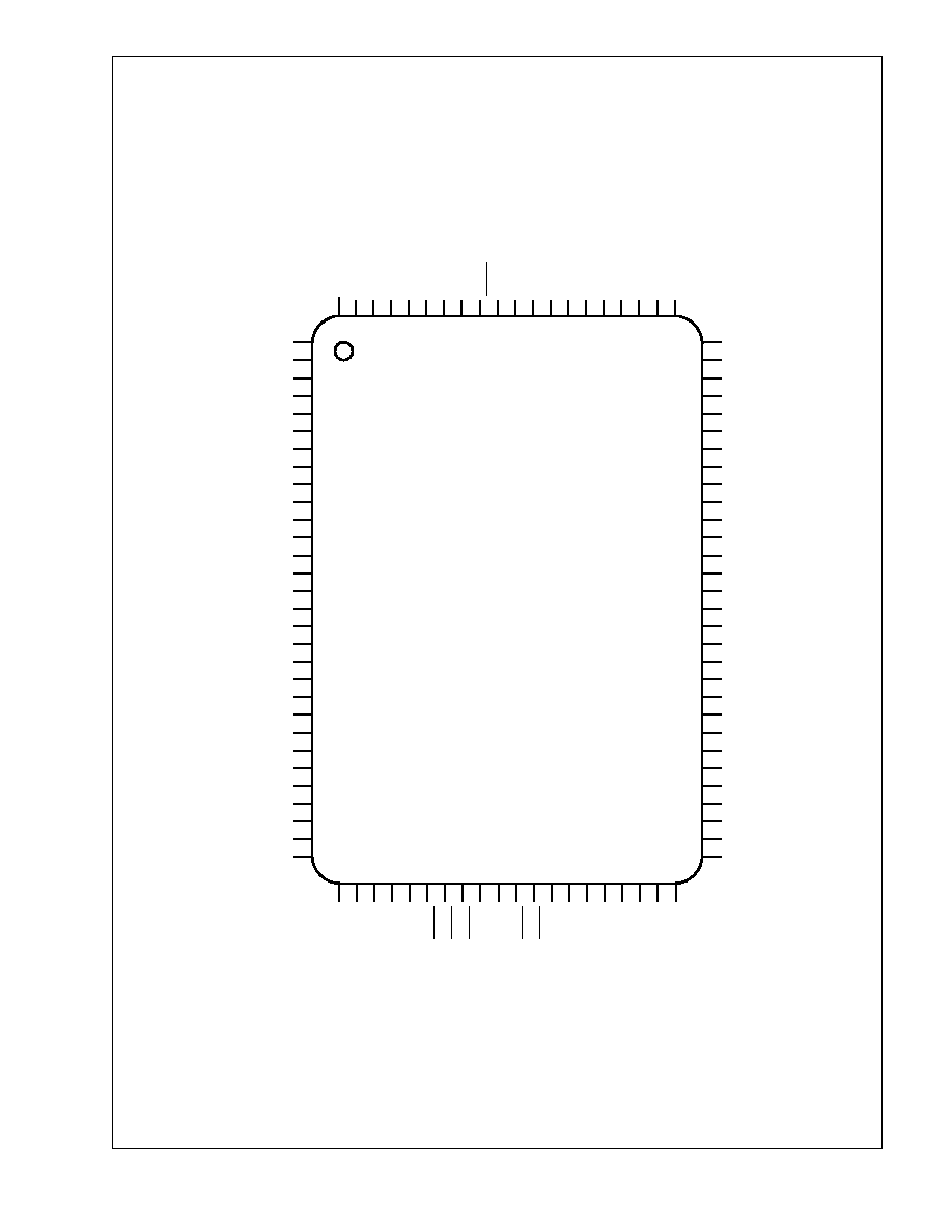
1.0 PIN CONNECTION DIAGRAM
2.0 PIN DESCRIPTION
2.1 MII Interface
2.2 100 Mb/s Serial PMD Interface
2.3 10 Mb/s Interface
2.4 Clock Interface
2.5 Device Configuration Interface
2.6 LED Interface
2.7 IEEE 1149.1 Interface
2.8 PHY Address Interface
2.9 Miscellaneous
2.10 Power and Ground Pins
2.11 Special Connect Pins
2.12
3.0 FUNCTIONAL DESCRIPTION
3.1 PCS Control
3.2 MII Serial Management Register Access
3.3 100BASE-X Transmitter
3.4 100BASE-X Receiver
3.5 Clock Generation Module
3.6 100 Mb/s Clock Recovery Module
3.7 10BASE-T Transceiver Module
3.8 IEEE 1149.1 Controller
3.9 IEEE 802.3u Auto-Negotiation
3.10 Reset Operation
3.11 Loopback Operation
3.12 Alternative 100BASE-X Operation
3.13 Low Power Mode
4.0 Registers
4.1 Key to Defaults
4.2 Basic Mode Control Register
4.3 Basic Mode Status Register
4.4 PHY Identifier Register #1
4.5 PHY Identifier Register #2
4.6 Auto-Negotiation Advertisement Register
4.7 Auto-Negotiation Link Partner Ability
Register
4.8 Auto-Negotiation Expansion Register
4.9 Disconnect Counter Register
4.10 False Carrier Sense Counter Register
4.11 Receive Error Counter Register
4.12 Silicon Revision Register
4.13 PCS Sub-Layer Configuration Register
4.14 Loopback, Bypass, and Receive Error
Mask Register
4.15 PHY Address Register
4.16 10BASE-T Status Register
4.17 10BASE-T Configuration Register
5.0 DP83840A APPLICATION
5.1 Typical Board Level Application
5.2 Layout Recommendations
5.3 Plane Partitioning
5.4 Power and Ground Filtering
6.0 Hardware User Information
6.1 Jabber/Timeout
6.2 Link Timer
6.3 Link LED, Link Status Bit
6.4 PHYAD[3] and Speed_100
6.5 Collision De-Assertion Time
6.6 Synchronization of Idle
6.7 100 Mb/s Differential Output Voltage
6.8 10Base-T Transmit Differential Output
Impedance
6.9 Low Power Mode
6.10 Software Reset
6.11 Receive Error Counter
6.12 Auto-Negotiation Test Compliancy
7.0 Software User information
7.1 100Mb/s Full Duplex Log-On
7.2 Auto-Negotiation to Link Sending 100Mb/
s Scrambled Idles
7.3 840A Auto-Negotiating to Legacy Devices
7.4 HBE Disable in 10Mb/s Repeater Mode
7.5 CRS Glitching in 10Mb/s Repeater Mode
8.0 ELECTRICAL SPECIFICATIONS
8.1 Ratings and Operating Conditions
8.2 DC Specifications
8.3 Clock Timing
8.4 MII Serial Management AC Timing
8.5 100 Mb/s AC Timing
8.6 10 Mb/s AC Timing
8.7 Fast Link Pulse Timing
8.8 Clock Recovery Module Timing
8.9 Reset Timing
8.10 Loopback Timing
8.11 PHY Isolation Timing
9.0 Package Dimensions
5
National Semiconductor
Subject to change without notice.
Version A
DP83840A 10/100 Mb/s Ethernet Physical Layer
2.0 Pin Description
The DP83840A pins are classified into the following interface categories (each interface is described in the sections that
follow):
MII INTERFACE
100 Mb/s SERIAL PMD INTERFACE
10 Mb/s INTERFACE
CLOCK INTERFACE
DEVICE CONFIGURATION INTERFACE
LED INTERFACE
IEEE 1149.1 INTERFACE
PHY ADDRESS INTERFACE
MISCELLANEOUS PINS
POWER AND GROUND PINS
SPECIAL CONNECT PINS
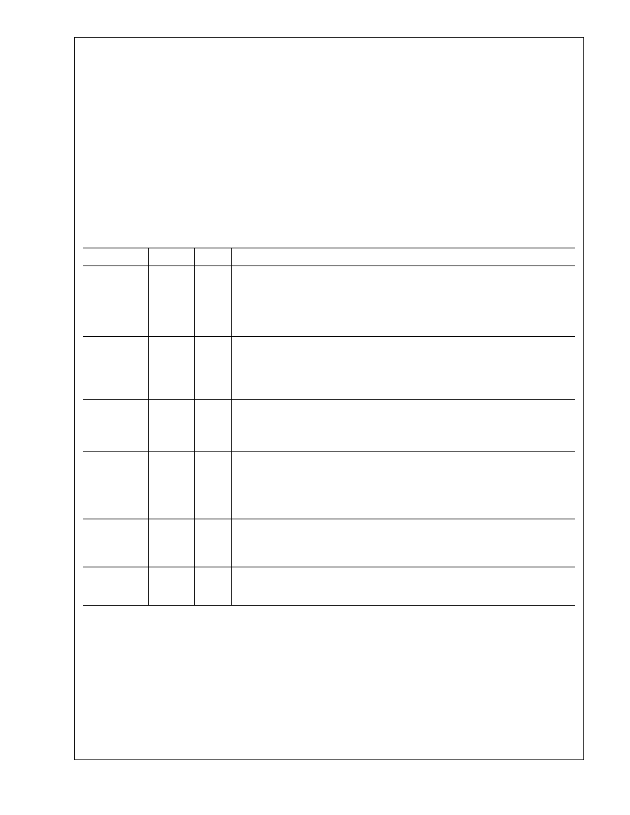
2.1 MII INTERFACE
Signal Name
Type
Pin #
Description
TX_CLK
O, Z
82
TRANSMIT CLOCK: Transmit clock output from the DP83840A:
25 MHz nibble transmit clock derived from Clock Generator Module's (CGM) PLL
in 100BASE-TX mode
2.5 MHz transmit clock in 10BASE-T nibble mode
10 MHz transmit clock in 10BASE-T serial mode
TXD[3]
TXD[2]
TXD[1]
TXD[0]
I, J
75
76
77
78
TRANSMIT DATA: Transmit data MII input pins that accept nibble data during
normal nibble-wide MII operation at either 2.5 MHz (10BASE-T mode) or 25MHz
(100BASE-X mode)
In 10 Mb/s serial mode, the TXD[0] pin is used as the serial data input pin. TXD[3:1]
are ignored.
TX_EN
I, J
74
TRANSMIT ENABLE: Active high input indicates the presence of valid nibble data
on TXD[3:0] for both 100 Mb/s or 10 Mb/s nibble mode.
In 10 Mb/s serial mode, active high indicates the presence of valid 10 Mb/s data on
TXD[0].
TX_ER
(TXD[4])
I, J
73
TRANSMIT ERROR: In 100 Mb/s mode, when this signal is high and TX_EN is
active the HALT symbol is substituted for the actual data nibble.
In 10 Mb/s mode, this input is ignored.
In encoder bypass mode (BP_4B5B or BP_ALIGN), TX_ER becomes the TXD [4]
pin, the new MSB for the transmit 5-bit data word.
MDC
I,J
72
MANAGEMENT DATA CLOCK: Synchronous clock to the MDIO management
data input/output serial interface which may be asynchronous to transmit and
receive clocks. The maximum clock rate is 2.5 MHz. There is no minimum clock
rate.
MDIO
I/O, Z, J
67
MANAGEMENT DATA I/O: Bi-directional management instruction/data signal that
may be sourced by the station management entity or the PHY. This pin requires a
1.5k
pullup resistor.
I = TTL/CMOS input
O = TTL/CMOS output
Z = TRI-STATE output
J = IEEE 1149.1 pin