1
National Semiconductor
Version A
March 1997
DP83840A 10/100 Mb/s Ethernet Physical Layer
General Description
The DP83840A is a Physical Layer device for Ethernet
10BASE-T and 100BASE-X using category 5 Unshielded,
Type 1 Shielded and Fiber Optic cables.
This VLSI device is designed for easy implementation of
10/100 Mb/s Ethernet LANs. It interfaces to the PMD sub-
layer through National Semiconductor's DP83223 Twisted
Pair Transceiver, and to the MAC layer through a Media
Independent Interface (MII), ensuring interoperability
between products from different vendors.
The DP83840A is designed with National Semiconductor's
BiCMOS process. Its system architecture is based on the
integration of several of National Semiconductor's industry
proven core technologies:
10BASE-T ENDEC/Transceiver module to provide the 10
Mb/s IEEE 802.3 functions
Clock Recovery/Generator Modules from National
Semiconductor's leading FDDI product
FDDI Stream Cipher (Cyclone)
100BASE-X physical coding sub-layer (PCS) and control
logic that integrate the core modules into a dual speed
Ethernet physical layer controller
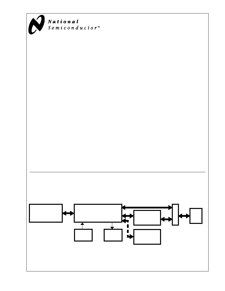
System Diagram
Features
∑
IEEE 802.3 10BASE-T compatible--ENDEC and UTP/
STP transceivers and filters built-in
∑
IEEE 802.3u 100BASE-X compatible--support for 2 pair
Category 5 UTP (100m), Type 1 STP and Fiber Optic
Transceivers--Connects directly to the DP83223 Twisted
Pair Transceiver
∑
ANSI X3T12 TP-PMD compatible
∑
IEEE 802.3u Auto-Negotiation for automatic speed
selection
∑
IEEE 802.3u compatible Media Independent Interface
(MII) with Serial Management Interface
∑
Integrated high performance 100 Mb/s clock recovery
circuitry requiring no external filters
∑
Full Duplex support for 10 and 100 Mb/s
∑
MII Serial 10 Mb/s output mode
∑
Fully configurable node and repeater modes--allows
operation in either application
∑
Programmable loopback modes for easy system
diagnostics
∑
Flexible LED support
∑
IEEE 1149.1 Standard Test Access Port and Boundary-
Scan compatible
∑
Small footprint 100-pin PQFP package
∑
Individualized scrambler seed for multi-PHY applications
DP83840A
10/100 Mb/s Ethernet Physical Layer
10 AND/OR 100 Mb/s
ETHERNET MAC OR
REPEATER/SWITCH
PORT
DP83840A
10/100 Mb/s
ETHERNET PHYSICAL LAYER
CLOCKS
STATUS
LEDS
DP83223
100BASE-TX
TRANSCEIVER
MA
GNETICS
RJ-45
10BASE-T
OR
100BASE-TX
MII
10BASE-T
100BASE-FX
TRANSCEIVER
2
National Semiconductor
Version A
DP83840A 10/100 Mb/s Ethernet Physical Layer
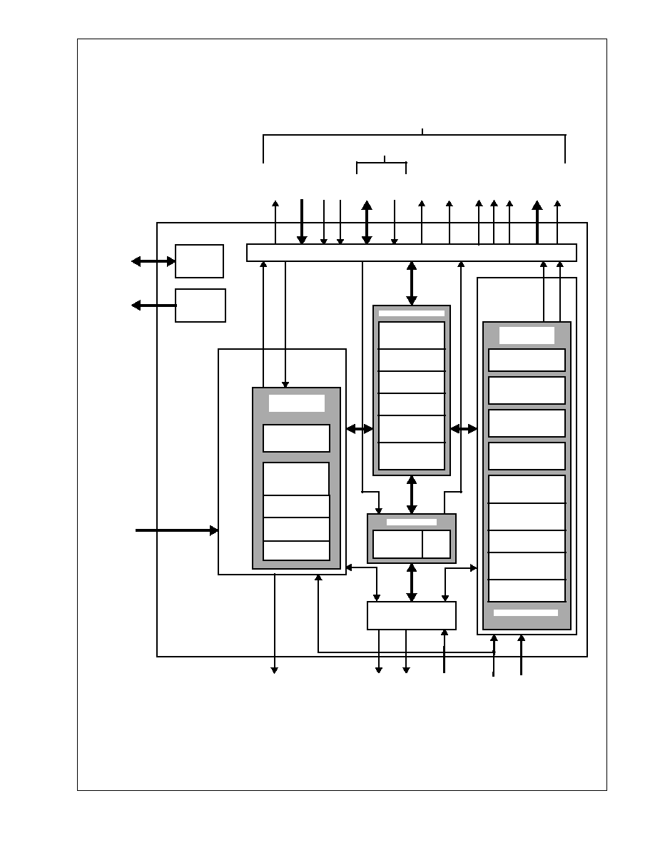
Block Diagram
SERIAL
MANAGEMENT
MII
IEEE
1149.1
(JTAG)
TX_CLK
TXD[3:0]
TX_ER
TX_EN
MDIO
MDC
COL
CRS
RX_ER
RX_D
V
RXD[3:0]
RX_CLK
MII INTERFACE/CONTROL
TEST
ACCESS
PORT
LED
DRIVERS
LED 1-5
100 Mb/s
RECEIVE
CLOCK
D
ATA
REGISTERS
AUTO
NEGOTIATION
RX STATE
MACHINE
PCS
SSD
DETECT
CARRIER
SENSE
COLLISION
DETECTION
CODE-GROUP
DECODER
CODE-GROUP
ALIGNMENT
DESCRAMBLER
RD +/-
SD +/-
SERIAL TO
PARALLEL
CRM
NRZI TO NRZ
100BASE-X
10BASE-T
MII
NODE/
REPEATER
PCS
CONTROL
10BASE-T
TX
UTP/STP
RX
AUTO
NEGOTIATION
100 Mb/s
RECEIVE
CLOCK
D
ATA
PCS
CODE-GROUP
ENCODER AND
INJECTION
SCRAMBLER
CLOCK(S)
PARALLEL TO
SERIAL
100BASE-X
RECEIVE INTERFACE
RXI +/-
TXS+/-
TXU+/-
TD +/-
100BASE-X
TRANSMIT INTERFACE
10 BASE-T
INTERFACE
CGM
NRZ / NRZI
TX STATE
MACHINE
RX_EN

3
Table of Contents
National Semiconductor
Version A
DP83840A 10/100 Mb/s Ethernet Physical Layer
GENERAL DESCRIPTION
FEATURES
SYSTEM DIAGRAM
BLOCK DIAGRAM
REVISION HISTORY
TABLE OF CONTENTS
1.0 PIN CONNECTION DIAGRAM
2.0 PIN DESCRIPTION
2.1 MII Interface
2.2 100 Mb/s Serial PMD Interface
2.3 10 Mb/s Interface
2.4 Clock Interface
2.5 Device Configuration Interface
2.6 LED Interface
2.7 IEEE 1149.1 Interface
2.8 PHY Address Interface
2.9 Miscellaneous
2.10 Power and Ground Pins
2.11 Special Connect Pins
2.12
3.0 FUNCTIONAL DESCRIPTION
3.1 PCS Control
3.2 MII Serial Management Register Access
3.3 100BASE-X Transmitter
3.4 100BASE-X Receiver
3.5 Clock Generation Module
3.6 100 Mb/s Clock Recovery Module
3.7 10BASE-T Transceiver Module
3.8 IEEE 1149.1 Controller
3.9 IEEE 802.3u Auto-Negotiation
3.10 Reset Operation
3.11 Loopback Operation
3.12 Alternative 100BASE-X Operation
3.13 Low Power Mode
4.0 Registers
4.1 Key to Defaults
4.2 Basic Mode Control Register
4.3 Basic Mode Status Register
4.4 PHY Identifier Register #1
4.5 PHY Identifier Register #2
4.6 Auto-Negotiation Advertisement Register
4.7 Auto-Negotiation Link Partner Ability
Register
4.8 Auto-Negotiation Expansion Register
4.9 Disconnect Counter Register
4.10 False Carrier Sense Counter Register
4.11 Receive Error Counter Register
4.12 Silicon Revision Register
4.13 PCS Sub-Layer Configuration Register
4.14 Loopback, Bypass, and Receive Error
Mask Register
4.15 PHY Address Register
4.16 10BASE-T Status Register
4.17 10BASE-T Configuration Register
5.0 DP83840A APPLICATION
5.1 Typical Board Level Application
5.2 Layout Recommendations
5.3 Plane Partitioning
5.4 Power and Ground Filtering
6.0 Hardware User Information
6.1 Jabber/Timeout
6.2 Link Timer
6.3 Link LED, Link Status Bit
6.4 PHYAD[3] and Speed_100
6.5 Collision De-Assertion Time
6.6 Synchronization of Idle
6.7 100 Mb/s Differential Output Voltage
6.8 10Base-T Transmit Differential Output
Impedance
6.9 Low Power Mode
6.10 Software Reset
6.11 Receive Error Counter
6.12 Auto-Negotiation Test Compliancy
7.0 Software User information
7.1 100Mb/s Full Duplex Log-On
7.2 Auto-Negotiation to Link Sending 100Mb/
s Scrambled Idles
7.3 840A Auto-Negotiating to Legacy Devices
7.4 HBE Disable in 10Mb/s Repeater Mode
7.5 CRS Glitching in 10Mb/s Repeater Mode
8.0 ELECTRICAL SPECIFICATIONS
8.1 Ratings and Operating Conditions
8.2 DC Specifications
8.3 Clock Timing
8.4 MII Serial Management AC Timing
8.5 100 Mb/s AC Timing
8.6 10 Mb/s AC Timing
8.7 Fast Link Pulse Timing
8.8 Clock Recovery Module Timing
8.9 Reset Timing
8.10 Loopback Timing
8.11 PHY Isolation Timing
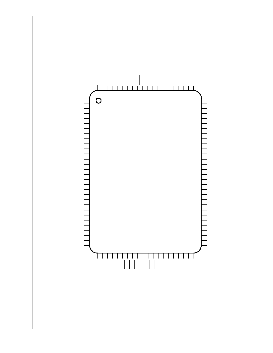
9.0 Package Dimensions
4
National Semiconductor
Subject to change without notice.
Version A
DP83840A 10/100 Mb/s Ethernet Physical Layer
2
1
4
3
BPSCR
OSCIN
LOWPWR
RES_0
6
5
8
7
RD+
RD-
SD-
SD+
10
9
12
11
ANAV
CC
ANAGND
CRMGND
CRMV
CC
14
13
16
15
NC
NC
ECLV
CC
TD-
TD+
RXV
CC
RXGND
RXI-
RXI+
TDV
CC
TXS-
TXS+
TXU-
TXU+
TDGND
RTX
REQ
PLLGND
18
17
20
19
22
21
24
23
26
25
28
27
30
29
81
CLK25M
TX_CLK
NC
REFV
CC
REFGND
REFIN
CGMV
CC
CGMGND
SPEED_100 / PHY
AD[3]
RES_0
TDI
TRST
TCLK
TMS
AN0
IO
V
CC1
IOGND1
10BTSER
BP
ALIGN
82
83
84
85
86
87
88
89
90
91
92
93
94
95
96
97
98
99
100
BP4B5B
50
49
48
47
46
45
44
43
42
41
40
39
38
37
36
35
34
33
32
31
79
80
77
78
75
76
73
74
71
72
69
70
67
68
65
66
63
64
61
62
59
60
57
58
55
56
53
54
51
52
IOGND6
IOV
CC6
TXD[0]
TXD[1]
TXD[2]
TXD[3]
TX_EN
TX_ER
MDC
PCSGND
PCSV
CC
IOGNDS
IOV
CC5
MDIO
CRS / PHYAD[2]
COL
RX_DV
RX_ER / PHYAD[4]
RX_CLK
RCLKGND
IOGND4
IOV
CC4
RXD[0]
RXD[1]
RXD[2]
RXD[3]
SPEED_10
ENCSEL / PHYAD[1]
IOGND3
IOV
CC3
TDO
LBEN / PHY
AD[0]
RES_0
REPEA
TER
AN1
RES_0
RESET
RX_EN
LED1
LED2
IOGND2
IO
V
CC2
LED3
LED4
LED5
OGND
X2
X1
OV
CC
PLL
V
CC
DP83840AVCE
10/100BASE-X ETHERNET PHYSICAL LAYER
100 -PIN JEDEC METRIC PQFP
FIGURE 1. DP83840A Pin Connection Diagram
2.0 Pin Connection Diagram

5
National Semiconductor
Subject to change without notice.
Version A
DP83840A 10/100 Mb/s Ethernet Physical Layer
2.0 Pin Description
The DP83840A pins are classified into the following interface categories (each interface is described in the sections that
follow):
MII INTERFACE
100 Mb/s SERIAL PMD INTERFACE
10 Mb/s INTERFACE
CLOCK INTERFACE
DEVICE CONFIGURATION INTERFACE
LED INTERFACE
IEEE 1149.1 INTERFACE
PHY ADDRESS INTERFACE
MISCELLANEOUS PINS
POWER AND GROUND PINS
SPECIAL CONNECT PINS
2.1 MII INTERFACE
Signal Name
Type
Pin #
Description
TX_CLK
O, Z
82
TRANSMIT CLOCK: Transmit clock output from the DP83840A:
25 MHz nibble transmit clock derived from Clock Generator Module's (CGM) PLL
in 100BASE-TX mode
2.5 MHz transmit clock in 10BASE-T nibble mode
10 MHz transmit clock in 10BASE-T serial mode
TXD[3]
TXD[2]
TXD[1]
TXD[0]
I, J
75
76
77
78
TRANSMIT DATA: Transmit data MII input pins that accept nibble data during
normal nibble-wide MII operation at either 2.5 MHz (10BASE-T mode) or 25MHz
(100BASE-X mode)
In 10 Mb/s serial mode, the TXD[0] pin is used as the serial data input pin. TXD[3:1]
are ignored.
TX_EN
I, J
74
TRANSMIT ENABLE: Active high input indicates the presence of valid nibble data
on TXD[3:0] for both 100 Mb/s or 10 Mb/s nibble mode.
In 10 Mb/s serial mode, active high indicates the presence of valid 10 Mb/s data on
TXD[0].
TX_ER
(TXD[4])
I, J
73
TRANSMIT ERROR: In 100 Mb/s mode, when this signal is high and TX_EN is
active the HALT symbol is substituted for the actual data nibble.
In 10 Mb/s mode, this input is ignored.
In encoder bypass mode (BP_4B5B or BP_ALIGN), TX_ER becomes the TXD [4]
pin, the new MSB for the transmit 5-bit data word.
MDC
I,J
72
MANAGEMENT DATA CLOCK: Synchronous clock to the MDIO management
data input/output serial interface which may be asynchronous to transmit and
receive clocks. The maximum clock rate is 2.5 MHz. There is no minimum clock
rate.
MDIO
I/O, Z, J
67
MANAGEMENT DATA I/O: Bi-directional management instruction/data signal that
may be sourced by the station management entity or the PHY. This pin requires a
1.5k
pullup resistor.
I = TTL/CMOS input
O = TTL/CMOS output
Z = TRI-STATE output
J = IEEE 1149.1 pin

2.0 Pin Description
(Continued)
6
National Semiconductor
Version A
DP83840A 10/100 Mb/s Ethernet Physical Layer
CRS
(PHYAD[2])
I/O, Z, J
66
CARRIER SENSE: This pin is asserted high to indicate the presence of carrier due
to receive or transmit activities in 10BASE-T or 100BASE-X Half Duplex modes.
In Repeater or Full Duplex mode a logic 1 indicates presence of carrier due only to
receive activity.
This is also the PHY address sensing (PHYAD[2]) pin for multiple PHY
applications--see Section 2.8 for further detail.
COL
O, Z, J
65
COLLISION DETECT: Asserted high to indicate detection of collision conditions in
10 Mb/s and 100 Mb/s Half Duplex modes.
During 10BASE-T Half Duplex mode with Heartbeat asserted (bit 4, register 1Ch),
this pin is also asserted for a duration of approximately 1
µ
s at the end of
transmission to indicate CD heartbeat.
In Full Duplex mode, for 10 Mb/s or 100 Mb/s operation, this signal is always logic
0. There is no heartbeat function during 10 Mb/s full duplex operation.
RX_CLK
O, Z
62
RECEIVE CLOCK: Provides the recovered receive clock for different modes of
operation:
∑
25 MHz nibble clock in 100 Mb/s mode
∑
2.5 MHz nibble clock in 10 Mb/s nibble mode
∑
10 MHz receive clock in 10 Mb/s serial mode
RX_ER
(RXD[4])
(PHYAD[4])
O, Z, J
63
RECEIVE ERROR: Asserted high to indicate that an invalid symbol has been
detected within a received packet in 100 Mb/s mode.
In decoder bypass mode (BP_4B5B or BP_ALIGN modes), RX_ER becomes
RXD[4], the new MSB for the receive 5-bit data word.
This is also the PHY address sensing (PHYAD) pin for multiple PHY applications--
see Section 2.8 for more details.
RX_DV
O, Z, J
64
RECEIVE DATA VALID: Asserted high to indicate that valid data is present on
RXD[3:0].
This pin is not meaningful during either transparent or phaser mode. Refer to
section 3.12 for further detail.
RXD[3]
RXD[2]
RXD[1]
RXD[0]
O, Z, J
55
56
57
58
RECEIVE DATA: Nibble wide receive data (synchronous to RX_CLK, 25 MHz for
100BASE-X mode, 2.5 MHz for 10BASE-T nibble mode). Data is driven on the
falling edge of RX_CLK.
In 10 Mb/s serial mode, the RXD[0] pin is used as the data output pin which is also
clocked out on the falling edge of RX_CLK. During 10 Mb/s serial mode RXD[3:1]
become don't care.
RX_EN
I, J
43
RECEIVE ENABLE: Active high enable for receive signals RXD[3:0], RX_CLK,
RX_DV and RX_ER. A low on this input tri-states these output pins. For normal
operation in a node application this pin should be pulled high.
2.2 100 Mb/s SERIAL PMD INTERFACE
Signal Name
Type
Pin #
Description
SPEED_10
O, J
54
SPEED 10 Mb/s: Indicates 10 Mb/s operation when high. Indicates 100 Mb/s
operation when low. This pin can be used to drive peripheral circuitry such as an
LED indicator or control circuits for common magnetics.
SPEED_100
(PHYAD[3])
I/O, J
89
SPEED 100 Mb/s: Indicates 100 Mb/s operation when high. Indicates 10 Mb/s
operation when low. This pin can be used to drive peripheral circuitry such as an
LED indicator or control circuits for common magnetics.
This is also the PHY address sensing (PHYAD[3]) pin for multiple PHY applications-
-see Section 2.8 for more details.
2.1 MII INTERFACE
I = TTL/CMOS input
O = TTL/CMOS output
Z = TRI-STATE output
J = IEEE 1149.1 pin

2.0 Pin Description
(Continued)
7
National Semiconductor
Version A
DP83840A 10/100 Mb/s Ethernet Physical Layer
ENCSEL
(PHYAD[1])
I/O, J
53
ENCODE SELECT: Used to select binary or MLT-3 coding scheme in the PMD
transceiver (at the DP83223, logic high selects binary coding scheme and logic low
selects MLT-3 coding scheme).
This is also the PHY address sensing (PHYAD[1]) pin for multiple PHY applications-
-see Section 2.8 for more details.
LBEN
(PHYAD[0])
I/O, J
49
LOOPBACK ENABLE: For 100BASE-TX operation, this pin should be connected
to the Loopback Enable pin of a DP83223 100 Mb/s Transceiver:
1 = local 100BASE-TX transceiver Loopback enabled
0 = local 100BASE-TX transceiver Loopback disabled (normal operation)
This is also the PHY address sensing (PHYAD[0]) pin for multiple PHY applications-
-see Section 2.8 for more details.
This pin has no effect during 10 Mb/s operation.
TD-
TD+
O (ECL)
16
17
TRANSMIT DATA: Differential ECL 125 Mb/s serialized transmit data outputs to
the PMD transceiver (such as the DP83223).
SD-
SD+
I (ECL)
7
8
SIGNAL DETECT: Differential ECL signal detect inputs. Indicates that the PMD
transceiver has detected a receive signal from the twisted pair or fiber media.
RD-
RD+
I (ECL)
6
5
RECEIVE DATA: Differential ECL 125 Mb/s receive data inputs from the PMD
transceiver (such as the DP83223).
2.3 10 Mb/s INTERFACE
Signal Name
Type
Pin #
Description
REQ
I
29
EQUALIZATION RESISTOR: A resistor connected between this pin and GND or
V
CC
adjusts the equalization step amplitude on the 10BASE-T Manchester
encoded transmit data (TXU+/- or TXS+/-). Typically no resistor is required for
operation with cable lengths less than 100m. Great care must be taken to ensure
system timing integrity when using cable lengths greater than 100m. Refer to the
IEEE 802.3u standard, Clause 29 for more details on system topology issues.
This value must be determined empirically. Refer to section 3.7.8 for further detail.
RTX
I
28
EXTENDED CABLE RESISTOR: A resistor connected between this pin and GND
or V
CC
adjusts the amplitude of the differential transmit outputs (TXU+/- or TXS+/-
). Typically no resistor is required for operation with cable lengths less than 100m.
Great care must be taken to ensure system timing integrity when using cable
lengths greater than 100m. Refer to the IEEE 802.3u standard, Clause 29 for more
details on system topology issues.
This value must be determined empirically. Refer to section 3.7.8 for further detail.
TXU-
TXU+
O
25
26
UNSHIELDED TWISTED PAIR OUTPUT: This differential output pair sources the
10BASE-T transmit data and link pulses for UTP cable.
TXS-
TXS+
O
23
24
SHIELDED TWISTED PAIR OUTPUT: This differential output pair sources the
10BASE-T transmit data and link pulses for STP cable.
RXI-
RXI+
I
20
21
TWISTED PAIR RECEIVE INPUT: These are the differential 10BASE-T receive
data inputs for either STP or UTP.
2.2 100 Mb/s SERIAL PMD INTERFACE
I = TTL/CMOS input
O = TTL/CMOS output
Z = TRI-STATE output
J = IEEE 1149.1 pin

2.0 Pin Description
(Continued)
8
National Semiconductor
Version A
DP83840A 10/100 Mb/s Ethernet Physical Layer
2.4 CLOCK INTERFACE
Signal Name
Type
Pin #
Description
REFIN
I
86
REFERENCE INPUT: 25 MHz TTL reference clock input. This clock can be
supplied from an external oscillator module or from the CLK25M output (pin 81).
CLK25M
O, Z
81
25 MHz CLOCK OUTPUT: Derived from the 50 MHz OSCIN input. When not in
use, this clock output may be shut off through software by setting bit 7 of the PCS
Configuration Register at address 17h. This output remains unaffected by
hardware and software reset.
OSCIN
I
2
OSCILLATOR INPUT: 50 MHz 50 ppm external TTL oscillator input. If not used,
pull down to GND (4.7 k
pull down resistor suggested).
X2
O
34
CRYSTAL OSCILLATOR OUTPUT: External 20 MHz 0.005% crystal
connection. Used for 10BASE-T timing. When using an external 20 MHz oscillator
connected to X1 or with no reference to X1, leave this pin unconnected.
X1
I
33
CRYSTAL OSCILLATOR INPUT: External 20 MHz 0.005% crystal connection.
Used for 10BASE-T timing and Auto-Negotiation. If not used, this pin should be
pulled up to V
CC.
(4.7 k
pull up resistor suggested). When pulled high, the
DP83840A detects this condition, enables the internal 2.5 divider, and switches
the 10 Mb/s and Auto-Negotiation circuitry to the internally derived 20 MHz clock.
I = TTL/CMOS input
O = TTL/CMOS output
Z = TRI-STATE output
J = IEEE 1149.1 pin

2.0 Pin Description
(Continued)
9
National Semiconductor
Version A
DP83840A 10/100 Mb/s Ethernet Physical Layer
2.5 DEVICE CONFIGURATION INTERFACE
Signal Name
Type
Pin #
Description
AN0
I
95
AN0: This is a quad state input pin (i.e, 1, M, 0, Clock) that works in conjunction
with the AN1 pin to control the forced or advertised operating mode of the
DP83840A according to the following table. The value on this pin is set by
connecting the input pin to GND (0), V
CC
(1), a continuous 25 MHz clock (C), or
leaving it unconnected (M.) The unconnected state, M, refers to the mid-level
(VCC2) set by internal resistors. This value is latched into the DP83840A at
power-up/reset. See section 3.9 for more details.
AN1
I
46
AN1: This is a quad-state input pin (i.e., 1, M, 0, Clock) that works in conjunction
with the AN0 pin to control the forced or advertised operating mode of the
DP83840A according to the table given in the AN0 pin description above. The
value on this pin is set by connecting the input pin to GND (0), V
CC
(1), a continuous
25 MHz clock (C), or leaving it unconnected (M.) This value is latched into the
DP83840A at power-up/reset. See Section 3.9 for more details.
REPEATER
I, J
47
REPEATER/NODE MODE: Selects REPEATER mode when set high and NODE
mode when set low. In REPEATER mode (or NODE mode with Full Duplex
configured), the Carrier Sense (CRS) output from the DP83840A is asserted due
to receive activity only. In NODE mode, and not configured for Full Duplex
operation, CRS is asserted due to either receive and transmit activity.
The Carrier Integrity Monitor (CIM) function is automatically disabled when this pin
is set low (node mode) and enabled when this pin is set high (Repeater mode) in
order to facilitate 802.3u /D5.3 CIM requirements.
At power-up/reset, the value on this pin (set by a pull-up or pull-down resistor,
typically 4.7 k
) is latched to bit 12 of the PCS Configuration Register, address
17h.
AN1
AN0
Forced Mode
0
M
10BASE-T, Half-Duplex without Auto-Negotiation
1
M
10BASE-T, Full Duplex without Auto-Negotiation
M
0
100BASE-TX, Half-Duplex without Auto-Negotiation
M
1
100BASE-TX, Full Duplex without Auto-Negotiation
C
M
100BASE-TX, Full Duplex without Auto-Negotiation
ANAR, register address 04h default modified
M
C
100BASE-TX, Full Duplex without Auto-Negotiation
ANAR, register address 04h default modified
C
C
100BASE-TX, Half Duplex without Auto-Negotiation
ANAR, register address 04h default modified
AN1
AN0
Advertised Mode
M
M
All capable (i.e. Full Duplex for 10BASE-T and 100BASE-
TX) advertised via Auto-Negotiation
0
0
10BASE-T, Half-Duplex advertised via Auto-Negotiation
0
1
10BASE-T, Full Duplex advertised via Auto-Negotiation
1
0
100BASE-TX, Half-Duplex advertised via Auto-Negotiation
1
1
100BASE-TX, Full Duplex advertised via Auto-Negotiation
C
1
100BASE-TX Full Duplex and 10BASE-T Full Duplex
advertised via Auto-Negotiation
C
0
100BASE-TX Half Duplex and 10BASE-T Half Duplex
advertised via Auto-Negotiation
1
C
100BASE-TX Half Duplex and 100BASE-TX Full Duplex
advertised via Auto-Negotiation
0
C
10BASE-T Half Duplex and 10BASE-T Full Duplex
advertised via Auto-Negotiation
I = TTL/CMOS input
O = TTL/CMOS output
Z = TRI-STATE output
J = IEEE 1149.1 pin

2.0 Pin Description
(Continued)
10
National Semiconductor
Version A
DP83840A 10/100 Mb/s Ethernet Physical Layer
10BTSER
I, J
98
SERIAL/NIBBLE SELECT:
10 Mb/s Serial Operation:
When set high, this input selects serial data transfer mode. Transmit and receive
data is exchanged serially at a 10 MHz clock rate on the least significant bits of the
nibble-wide MII data buses, pins TXD[0] and RXD[0] respectively. This mode is
intended for use with the DP83840A connected to a device (MAC or Repeater)
using a 10 Mb/s serial interface. Serial operation is not supported in 100 Mb/s
mode, therefore this input is ignored during 100 Mb/s operation
10 and 100 Mb/s Nibble Operation:
When set low, this input selects the MII compliant nibble data transfer mode.
Transmit and receive data is exchanged in nibbles on the TXD[3:0] and RXD[3:0]
pins respectively.
At power-up/reset, the value on this pin (set by a pull-up or pull-down resistor,
typically 4.7 k
) is latched into bit 9 of the 10BASE-T Status Register at address
1Bh.
BPALIGN
I, J
99
BYPASS ALIGNMENT: Allows 100 Mb/s transmit and receive data streams to
bypass all of the transmit and receive operations when set high. Refer to Figures 4
and 5. Note that the PCS signaling (CRS, RX_DV, RX_ER, and COL) is not
meaningful during this mode. Additionally TXD[4]/TX_ER is always active.
At power-up/reset, the value on this pin (set by a pull-up or pull-down resistor,
typically 4.7 k
) is latched into bit 12 of the Loopback, Bypass and Receiver Error
Mask Register at address 18h.
BP4B5B
I, J
100
BYPASS 4B5B ENCODER/DECODER: Allows 100 Mb/s transmit and receive
data streams to bypass the 4B to 5B encoder and 5B to 4B decoder circuits when
set high. All PCS signaling (CRS, RX_DV, RX_ER, and COL) remain active and
unaffected by this bypass mode. Additionally, TXD[4]/TX_ER is gated by TX_EN.
Refer to figures 4 and 5.
At power-up/reset, the value on this pin (set by a pull-up or pull-down resistor,
typically 4.7 k
) is latched into bit 14 of the Loopback, Bypass and Receiver Error
Mask Register at address 18h.
BPSCR
I, J
1
BYPASS SCRAMBLER/DESCRAMBLER: Allows 100 Mb/s transmit and receive
data streams to bypass the scrambler and descrambler circuits when set high to
facilitate 100BASE-FX operation. All PCS signaling (CRS, RX_DV, RX_ER, and
COL) remain active and unaffected by this bypass mode. Refer to figures 4 and 5.
At power-up/reset, the value on this pin (set by a pull-up or pull-down resistor,
typically 4.7 k
) is latched into bit 13 of the Loopback, Bypass and Receiver Error
Mask Register at address 18h.
2.5 DEVICE CONFIGURATION INTERFACE
I = TTL/CMOS input
O = TTL/CMOS output
Z = TRI-STATE output
J = IEEE 1149.1 pin
2.0 Pin Description
(Continued)
11
National Semiconductor
Version A
DP83840A 10/100 Mb/s Ethernet Physical Layer
2.6 LED INTERFACE
These outputs can be used to drive LEDs directly, or can be used to provide status information to a network
management device. Refer to Figure 12 for the LED connection diagram. Refer to section 2.2 for a description of how to
generate LED indication of 100 Mb/s mode. Note that these outputs are standard CMOS voltage drivers and not
open-drain.
Signal Name
Type
Pin #
Description
LED1
O, J
42
TRANSMIT LED: Indicates the presence of transmit activity (TXE asserted) for 10
Mb/s and 100 Mb/s operation. Active low.
If bit 2 (LED1_MODE) of the PCS Configuration Register (address 17h) is set
high, then the LED1 pin function is changed to indicate the status of the
Disconnect Function as defined by the state of bit 5 (CON_STATUS) in the PHY
address register (address 19h).
The DP83840A incorporates a "monostable" function on the LED1 output. This
ensures that even minimum size packets generate adequate LED ON time
(approximately 50ms) for visibility.
LED2
O, J
41
RECEIVE LED: Indicates the presence of any receive activity (CRS active) for 10
Mb/s and 100 Mb/s operation. Active low.
The DP83840A incorporates a "monostable" function on the LED2 output. This
ensures that even minimum size packets generate adequate LED ON time
(approximately 50ms) for visibility.
LED3
O, J
38
LINK LED: Indicates Good Link status for 10 Mb/s and 100 Mb/s operation. Active
low.
100 Mb/s Link is established as a result of the assertion of the Signal Detect input
to the DP83840A. LED3 will assert after SD has remained asserted for a minimum
of 500
µ
s. LED3 will deassert immediately following the deassertion of Signal
Detect.
10 Mb/s Link is established as a result of the reception of at least seven
consecutive normal Link Pulses or the reception of a valid 10BASE-T packet
which will cause the assertion of LED3. LED3 will deassert in accordance with the
Link Loss Timer as specified in 802.3.
LED4
O, J
37
POLARITY/FULL DUPLEX LED: Indicates Good Polarity status for 10 Mb/s
operation. Can be configured to Indicate Full Duplex mode status for 10 Mb/s or
100 Mb/s operation. Active low.
The DP83840A automatically compensates for polarity inversion. Polarity
inversion is indicated by the assertion of LED4.
If bit 1 (LED4_MODE) in the PCS Configuration Register (address 17h) is set
high, the LED4 pin function is changed to indicate Full Duplex mode status for 10
Mb/s and 100 Mb/s operation.
LED5
O, J
36
COLLISION LED: Indicates the presence of collision activity for 10 Mb/s and 100
Mb/s Half Duplex operation. This LED has no meaning for 10 Mb/s or 100 Mb/s
Full Duplex operation and will remain deasserted. Active low.
I = TTL/CMOS input
O = TTL/CMOS output
Z = TRI-STATE output
J = IEEE 1149.1 pin

2.0 Pin Description
(Continued)
12
National Semiconductor
Version A
DP83840A 10/100 Mb/s Ethernet Physical Layer
2.7 IEEE 1149.1 INTERFACE
The IEEE 1149.1 Standard Test Access Port and Boundary Scan (sometimes referred to as JTAG) interface signals
allow system level boundary scan to be performed. These pins may be left floating when JTAG testing is not required.
Signal Name
Type
Pin #
Description
TDO
O, Z
50
TEST DATA OUTPUT: Serial instruction/test output data for the IEEE 1149.1
scan chain.
If Boundary-Scan is not implemented this pin may be left unconnected (NC).
TDI
I
91
TEST DATA INPUT: Serial instruction/test input data for the IEEE 1149.1 scan
chain.
TRST
I
92
TEST RESET: An asynchronous low going pulse will reset and initialize the IEEE
1149.1 test circuitry.
If Boundary-Scan is not implemented, this pin may be left unconnected (NC) since
it has an internal pull-up resistor (10 k
).
TCLK
I
93
TEST CLOCK: Test clock for the IEEE 1149.1 circuitry.
If Boundary-Scan is not implemented this pin may be left unconnected (NC).
TMS
I
94
TEST MODE SELECT: Control input to the IEEE 1149.1 test circuitry.
If Boundary-Scan is not implemented, this pin may be left unconnected (NC) since
it has an internal pull-up resistor (10 k
).
I = TTL/CMOS input
O = TTL/CMOS output
Z = TRI-STATE output
J = IEEE 1149.1 pin

2.0 Pin Description
(Continued)
13
National Semiconductor
Version A
DP83840A 10/100 Mb/s Ethernet Physical Layer
2.8 PHY ADDRESS INTERFACE
The DP83840A PHYAD[4:0] inputs provide up to 32 unique PHY address options. An address selection of all zeros
(00000) will result in a PHY isolation condition. See the Isolate bit description in the BMCR, address 00h, Section 4.2
for further detail.
Signal Name
Type
Pin #
Description
PHYAD[0]
(LBEN)
I/O, J
49
PHY ADDRESS [0]: PHY address sensing pin (bit 0) for multiple PHY
applications. PHY address sensing is achieved by strapping a pull-up/pull-down
resistor (typically 4.7 k
) to this pin as required.
The pull-up/pull-down status of this pin is latched into the PHYAD address register
(address 19h) during power up/reset.
This pin is also the Loopback Enable output pin (LBEN) for the 100 Mb/s Serial
PMD Interface. See Section 2.2 for further detail.
PHYAD[1]
(ENCSEL)
I/O, J
53
PHY ADDRESS [1]: PHY address sensing pin (bit 1) for multiple PHY
applications. PHY address sensing is achieved by strapping a pull-up/pull-down
resistor (typically 4.7 k
) to this pin as required.
The pull-up/pull-down status of this pin is latched into the PHYAD address register
(address 19h) during power up/reset.
This pin is also the Encode Select output pin (ENCSEL) for the 100 Mb/s Serial
PMD Interface. See Section 2.2 for further detail.
PHYAD[2]
(CRS)
I/O, Z, J
66
PHY ADDRESS [2]: PHY address sensing pin (bit 2) for multiple PHY
applications. PHY address sensing is achieved by strapping a pull-up/pull-down
resistor (typically 4.7 k
) to this pin as required.
The pull-up/pull-down status of this pin is latched into the PHYAD address register
(address 19h) during power up/reset.
This pin is also the Carrier Sense output pin (CRS) for the MII Interface. See
Section 2.1 for further detail.
PHYAD[3]
(SPEED_100)
I/O, J
89
PHY ADDRESS [3]: PHY address sensing pin (bit 3) for multiple PHY
applications. PHY address sensing is achieved by strapping a pull-up/pull-down
resistor (typically 4.7 k
) to this pin as required.
The pull-up/pull-down status of this pin is latched into the PHYAD address register
(address 19h) during power up/reset.
This pin is also the Speed 100 Mb/s output pin (SPEED_100) for optional control
of peripheral circuitry. See Section 2.2 for further detail.
PHYAD[4]
(RX_ER)
I/O, Z, J
63
PHY ADDRESS [4]: PHY address sensing pin (bit 4) for multiple PHY
applications. PHY address sensing is achieved by strapping a pull-up/pull-down
resistor (typically 4.7 k
) to this pin as required.
The pull-up/pull-down status of this pin is latched into the PHYAD address register
(address 19h) during power up/reset.
This pin is also the Receive Error output pin (RX_ER) for the MII Interface. See
Section 2.1 for further detail.
2.9 MISCELLANEOUS
Signal Name
Type
Pin #
Description
RESET
I, J
44
RESET: Active high input that initializes or reinitializes the DP83840A. See
section 3.10 for further detail.
LOWPWR
I, J
3
LOW POWER MODE SELECT: Active high input that enables the low power
mode (100 Mb/s operation only). See section 3.13 for further detail.
I = TTL/CMOS input
O = TTL/CMOS output
Z = TRI-STATE output
J = IEEE 1149.1 pin

14
National Semiconductor
Version A
2.10 POWER AND GROUND PINS
The power (V
CC
) and ground (GND) pins of the DP83840A are grouped in pairs into four categories--TTL/CMOS Input
pairs, TTL/CMOS Output and I/O pairs, 10 Mb/s pairs and 100 Mb/s pairs. This grouping allows for optimizing the layout
and filtering of the power and ground supplies to this device. Refer to section 5.0 for further detail relating to power
supply filtering.
Signal Name
Pin #
Description
GROUP A - TTL/CMOS INPUT SUPPLY PAIRS
IOVCC1, IOGND1
96, 97
TTL Input/Output Supply #1
IOVCC2, IOGND2
39, 40
TTL Input/Output Supply #2
IOVCC3, IOGND3
51, 52
TTL Input/Output Supply #3
PCSVCC, PCSGND
70, 71
Physical Coding Sublayer Supply
GROUP B- TTL/CMOS OUTPUT AND I/O SUPPLY PAIRS
IOVCC4, IOGND4
59, 60
TTL Input/Output Supply #4
RCLKGND
61
Receive Clock Ground, No paired V
CC
IOVCC5, IOGND5
68, 69
TTL Input/Output Supply #5
IOVCC6, IOGND6
79, 80
TTL Input/Output Supply #6
REFVCC, REFGND
84, 85
25 MHz Clock Supply
GROUP C- 10 Mb/s SUPPLY PAIRS
RXVCC, RXGND
18, 19
Receive Section Supply
TDVCC, TDGND
22, 27
Transmit Section Supply
PLLVCC, PLLGND
31, 30
Phase Locked Loop Supply
OVCC, OGND
32, 35
Internal Oscillator Supply
GROUP D- 100 Mb/s SUPPLY PAIRS
ANAVCC, ANAGND
9, 10
Analog Section Supply
CRMVCC, CRMGND
12, 11
Clock Recovery Module Supply
ECLVCC
15
ECL Outputs Supply
CGMVCC, CGMGND
87, 88
Clock Generator Module Supply
2.11 SPECIAL CONNECT PINS
Signal Name
Type
Pin #
Description
NC
13
14
83
NO CONNECT: These pins are reserved for future use. Leave them unconnected
(floating).
RES_0
4
RESERVED_0: These pins are reserved for future use. This pin must be
connected to ground. For future upgradability, connect this pin to GND via a 0
resistor.
RES_0
J
45
48
90
RESERVED_0: These pins are reserved for future use. These pins must be
connected to ground. For future upgradability, connect these pins to GND via 0
resistors.
I = TTL/CMOS input
O = TTL/CMOS output
Z = TRI-STATE output
J = IEEE 1149.1 pin

15
National Semiconductor
Version A
DP83840A 10/100 Mb/s Ethernet Physical Layer
3.0 Functional Description
The DP83840A 10/100 Mb/s Ethernet Physical Layer
integrates a 100BASE-X Physical Coding Sub-layer (PCS)
and a complete 10BASE-T module in a single chip. It
provides a standard Media Independent Interface (MII) to
communicate between the Physical Signaling and the
Medium Access Control (MAC) layers for both 100BASE-X
and 10BASE-T operations. It interfaces to a 100 Mb/s
Physical Medium Dependent (PMD) transceiver, such as
the DP83223.
The 100BASE-X section of the device consists of the
following functional blocks:
∑
Transmitter
∑
Receiver
∑
Clock Generation Module (CGM)
∑
Clock Recovery Module (CRM)
The 10BASE-T section of the device consists primarily of
the 10 Mb/s transceiver module with filters and an ENDEC
module.
The 100BASE-X and 10BASE-T sections share the
following functional blocks:
∑
PCS Control
∑
MII Registers
∑
IEEE 1149.1 Controller
∑
IEEE 802.3u Auto-Negotiation
A description of each of these functional blocks follows.
3.1 PCS CONTROL
The IEEE 802.3u 100BASE-X Standard defines the
Physical Coding Sublayer (PCS) as the transmit, receive
and carrier sense functions. These functions within the
DP83840A are controlled via external pins and internal
registers via the MII serial management interface.
3.1.1 100BASE-X Bypass Options
The DP83840A incorporates a highly flexible transmit and
receive channel architecture. Each of the major 100BASE-
X transmit and receive functional blocks of the DP83840A
may be selectively bypassed to provide increased flexibility
for various applications.
3.1.1.1 Bypass 4B5B and 5B4B
The 100BASE-X 4B5B code-group encoder in the transmit
channel and the 100BASE-X 5B4B code-group decoder in
the receive channel may be bypassed by setting the
BP_4B5B bit in the LBREMR (bit 14, register address 18h).
The default value for this bit is set by the BP4B5B pin 100
at power-up/reset. This mode of operation is referred to as
the "Transparent" mode as further defined in section 3.12.
3.1.1.2 Bypass Scrambler and Descrambler
The 100BASE-T scrambler in the transmit channel and the
100BASE-T descrambler in the receive channel may be
bypassed by setting the BP_SCR bit in the LBREMR (bit
13, register address 18h). The default value for this bit is
set by the BPSCR signal (pin 1) at power-up/reset. This
bypass option has been included to facilitate 100BASE-FX
operation where data scrambling is not required.
3.1.1.3 Bypass NRZI Encoder and Decoder
The 100BASE-X NRZI encoder in the transmit channel and
the 100BASE-X NRZI decoder in the receive channel may
be bypassed by setting the NRZI_EN bit in the PCR (bit 15,
register address 17h). The default for this bit is a 1, which
enables the NRZI encoder and decoder. This bypass
option has been included for test purposes only and should
not be selected during normal 100BASE-X operation.
3.1.1.4 Bypass Align
The 100BASE-X transmit channel operations (4B5B code-
group encoder, scrambler and NRZ to NRZI) and the
100BASE-X receive channel operations (NRZI to NRZ,
descrambler and 4B5B code-group decoding) may all be
bypassed by setting the BP_ALIGN bit in the LBREMR (bit
12, register address 18h). The default value for this bit is
set by the BP_ALIGN signal (pin 99) at power-up/reset.
The bypass align function is intended for those repeater
applications where none of the transmit and receive
channel operations are required. This mode of operation is
referred to as the "Phaser" mode as further defined in
section 3.12
3.1.2 Repeater Mode
The DP83840A Carrier Sense (CRS) operation depends
on the value of the REPEATER bit in the PCR (bit 12,
register address 17h). When set high, the CRS output (pin
66) is asserted for receive activity only. When set low, the
CRS output is asserted for either receive or transmit
activity. The default value for this bit is set by the
REPEATER pin 47 at power-up/reset.
When the Repeater mode of operation is selected during
10 Mb/s operation, all functional parameters other than
CRS remain unaffected. CRS will respond only to receive
activity during 10 Mb/s repeater mode.
When the repeater mode of operation is selected during
100 Mb/s operation, there are three parameters that are
directly effected. First, as with 10 Mb/s Repeater operation,
CRS will only respond to receive activity.
Second, in compliance with D5 of the 802.3 standard, the
Carrier Integrity Monitor (CIM) function is automatically
enabled for detection and reporting of bad start of stream
delimiters (whereas in node mode the CIM is disabled).
Finally, the deassertion of CRS during the reception of a
long Jabber event is effected by the selection of the
repeater mode. If the repeater mode is selected, CRS will
remain asserted even if a long Jabber event (>722us)
occurs. This facilitates proper handling of a jabber event by
the Repeater Controller device. This Jabber related CRS
function can be over-ridden. Refer to section 4.15 (bit 11 of
register 19h) for further detail.
3.1.3 MII Control
The DP83840A provides three basic MII modes of
operation:
3.1.3.1 100 Mb/s Operation
For 100 Mb/s operation, the MII operates in nibble mode
with a clock rate of 25 MHz. This clock rate is independent
of bypass conditions.
In normal (non-bypassed) operation the MII data at
RXD[3:0] and TXD[3:0] is nibble wide. In bypass mode
(BP_4B5B or BP_ALIGN set) the MII data takes the form of
3.0 Functional Description
(Continued)
16
National Semiconductor
Version A
DP83840A 10/100 Mb/s Ethernet Physical Layer
5-bit code-groups. The lower significant 4 bits appear on
TXD[3:0] and RXD[3:0] as normal, and the most significant
bits (TXD[4] and RXD[4]) appear on the TX_ER and
RX_ER pins respectively.
3.1.3.2 10 Mb/s Nibble Mode Operation
For 10 Mb/s nibble mode operation, the MII clock rate is 2.5
MHz. The 100BASE-X bypass functions do not apply to 10
Mb/s operation.
3.1.3.3 10 Mb/s Serial Mode Operation
For applications based on serial repeater controllers for 10
Mb/s operation, the DP83840A accepts NRZ serial data on
the TXD[0] input and provides NRZ serial data output on
RXD[0] with a clock rate of 10 MHz. The unused MII inputs
and outputs (TXD[3:1] and RXD[3:1] are ignored during
serial mode. The PCS control signals, CRS, COL, TX_ER,
RX_ER, and RX_DV, continue to function normally.
This mode is selected by setting the 10BT_SER bit in the
10BTSR (bit 9, register address 1Bh). The default value for
this bit is set by the 10BTSER pin 98 at power-up/reset.
3.2 MII SERIAL MANAGEMENT REGISTER
ACCESS
The MII specification defines a set of thirty-two 16-bit
status and control registers that are accessible through the
serial management data interface pins MDC and MDIO.
The DP83840A implements all the required MII registers
as well as several optional registers. These registers are
fully described in Section 4. A description of the serial
management access protocol follows.
3.2.1 Serial Management Access Protocol
The serial control interface consists of two pins,
Management Data Clock (MDC) and Management Data
Input/Output (MDIO). MDC has a maximum clock rate of
2.5 MHz and no minimum rate. The MDIO line is bi-
directional and may be shared by up to 32 devices. The
MDIO frame format is shown in Table I.
The MDIO pin requires a pull-up resistor (1.5K
) which,
during IDLE and Turnaround, will pull MDIO high. Prior to
initiating any transaction, the station management entity
sends a sequence of 32 contiguous logic ones on MDIO to
provide the DP83840A with a sequence that can be used
to establish synchronization. This preamble may be
generated either by driving MDIO high for 32 consecutive
MDC clock cycles, or by simply allowing the MDIO pull-up
resistor to pull the MDIO PHY pin high during which time
32 MDC clock cycles are provided.
The DP83840A waits until it has received this preamble
sequence before responding to any other transaction.
Once the DP83840A serial management port has
initialized no further preamble sequencing is required until
after a Reset/Power-on has occurred.
The Start code is indicated by a <01> pattern. This assures
the MDIO line transitions from the default idle line state.
Turnaround is an idle bit time inserted between the
Register Address field and the Data field. To avoid
contention, no device actively drives the MDIO signal
during the first bit of Turnaround during a read transaction.
The addressed DP83840A drives the MDIO with a zero for
MDC
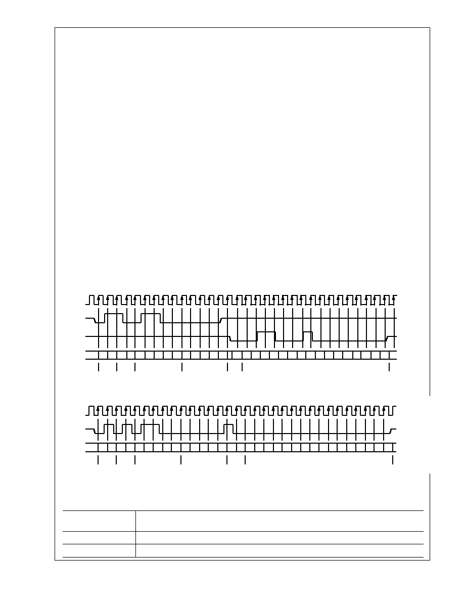
MDIO
0
0 0
1 1
1 1 0 0 0 0 0 0 0
(STA)
Idle
Start
Opcode
(Read)
PHY Address
(PHYAD = 0Ch)
Register Address
(00h = BMCR)
TA
Register Data
Z
MDIO
(PHY)
Z
Z
Z
0 0 0 1 1 0 0 0 1 0 0 0 0 0 0 0 0
Z
Idle
Z
Z
MDC
MDIO
0
0
0
1
1
1 1 0 0 0 0 0 0 0
(STA)
Idle
Start
Opcode
(Write)
PHY Address
(PHYAD = 0Ch)
Register Address
(00h = BMCR)
TA
Register Data
Z
0 0 0
0 0 0
0 0 0 0 0 0 0 0
Z
Idle
1
0 0
0
Z
Z
FIGURE 2. Typical MDC/MDIO Read Operation
FIGURE 3. Typical MDC/MDIO Write Operation
Table I.
MII Management
Serial Protocol
<idle><start><op code><device addr> <reg addr><turnaround><data><idle>
Read Operation
<idle><01><10><AAAAA> <RRRRR><Z0><xxxx xxxx xxxx xxxx><idle>
Write Operation
<idle><01><01><AAAAA> <RRRRR><10><xxxx xxxx xxxx xxxx><idle>

3.0 Functional Description
(Continued)
17
National Semiconductor
Version A
DP83840A 10/100 Mb/s Ethernet Physical Layer
the second bit of Turnaround and follows this with the
required data. Figure 2 shows the timing relationship
between MDC and the MDIO as driven/received by the
Station Management Entity (STA) and the DP83840A
(PHY) for a typical register read access.
For write transactions, the station management entity
writes data to an addressed DP83840A eliminating the
requirement for MDIO Turnaround. The Turnaround time is
filled by the management entity inserting <10> for these
two bits. Figure 3 shows the timing relationship for a typical
MII register write access.
3.2.1.1 Preamble Suppression
The DP83840A supports a Preamble Suppression mode
as indicated by a one in bit 6 of the Basic Mode Status
Register (BMSR, address 01h.) If the station management
entity (i.e. MAC or other management controller)
determines that all PHYs in the system support Preamble
Suppression by returning a one in this bit, then the station
management entity need not generate preamble for each
management transaction.
The DP83840A requires a single initialization sequence of
32 bits of preamble following power-up/hardware reset.
This requirement is generally met by the mandatory pull-up
resistor on MDIO or the management access made to
determine whether Preamble Suppression is supported.
While the DP83840A will respond to management
accesses without preamble,
a minimum of one idle bit
between management transactions is required as specified
in IEEE 802.3u.
3.2.2 PHY Address Sensing
The DP83840A can be set to respond to any of the
possible 32 PHY addresses. Each DP83840A connected
to a common serial MII must have a unique address. It
should be noted that while an address selection of all zeros
<00000> will result in PHY Isolate mode, this will not effect
serial management access.
The DP83840A provides five PHY address pins, the state
of which are latched into the PHY Address Register (PAR)
at system power-up/reset. These pins are described in
Section 2.8. For further detail relating to the latch-in timing
requirements of the PHY Address pins, as well as the other
hardware configuration pins, refer to section 3.10.
3.2.3 MII Management
The MII may be used to connect PHY devices to MAC or
repeater devices in 10/100 Mb/s systems.
The management interface of the MII allows the
configuration and control of multiple PHY devices, the
gathering of status and error information, and the
determination of the type and abilities of the attached
PHY(s).
3.2.4 MII Isolate Mode
A 100BASE-X PHY connected to the mechanical MII
interface specified in IEEE 802.3u is required to have a
default value of one in bit 10 of the Basic Mode Control
Register (BMCR, address 00h.) The DP83840A will set this
bit to one if the PHY Address is set to 00000 upon power-
up/hardware reset. Otherwise, the DP83840A will set this
bit to zero upon power-up/hardware reset.
With bit 10 in the BMCR set to one the DP83840A does not
respond to packet data present at TXD[3:0], TX_EN, and
TX_ER inputs and presents a high impedance on the
TX_CLK, RX_CLK, RX_DV, RX_ER, RXD[3:0], COL, and
CRS outputs. The CLK_25M output remains active and the
DP83840A will continue to respond to all management
transactions.
While in Isolate mode, the TD +/-, TXU +/-, and TXS +/-
outputs will not transmit packet data. However, the
DP83840A will default to 100 Mb/s mode and source
100BASE-X Idles during the Isolate condition. Data
present on the RD +/- and RXI +/- inputs is ignored and the
link will be forced to disable.
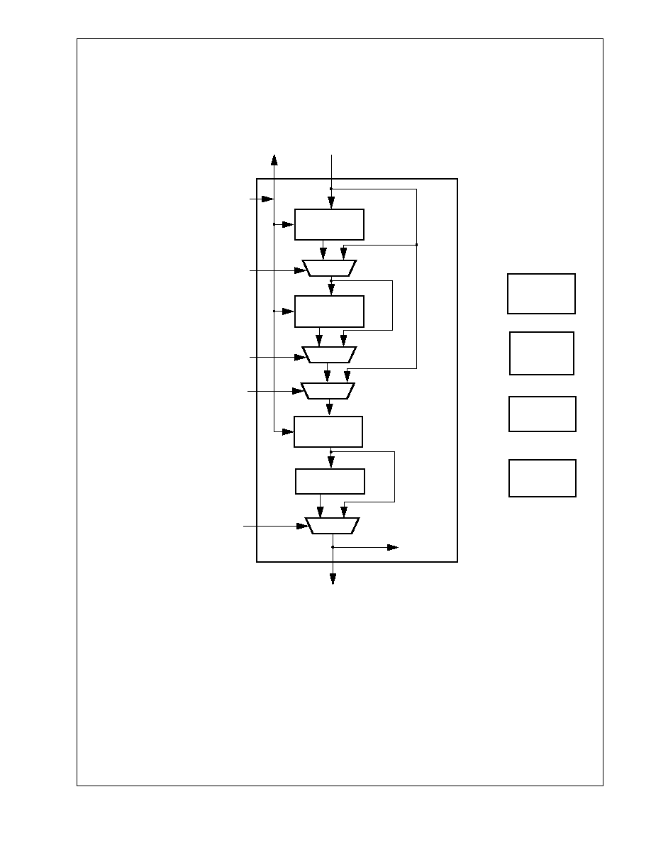
3.3 100BASE-X TRANSMITTER
The 100BASE-X transmitter consists of functional blocks
which convert synchronous 4-bit nibble data, as provided
by the MII, to a scrambled 125 Mb/s serial data stream.
This data stream may be routed either to a twisted pair
PMD such as the DP83223 TWISTER for 100BASE-TX
signaling, or to an optical PMD for 100BASE-FX
applications. The block diagram in Figure 4 provides an
overview of each functional block within the 100BASE-X
transmit section.
The Transmitter section consists of the following functional
blocks:
∑
code-group Encoder and Injection block (bypass option)
∑
Scrambler block (bypass option)
∑
NRZ to NRZI encoder block (bypass option)
The bypass option for each of the functional blocks within
the 100BASE-X transmitter provides flexibility for
applications such as 100 Mb/s repeaters where data
conversion is not always required.
3.3.1 100 Mb/s Transmit State Machine
The DP83840A implements the 100BASE-X transmit state
machine diagram as given in the IEEE 802.3u Standard,
Clause 24.
3.3.2 Code-group Encoding and Injection
The code-group encoder converts 4 bit (4B) nibble data
generated by the MAC into 5 bit (5B) code-groups for
transmission. This conversion is required to allow control
data to be combined with packet data code-groups. Refer
to Table II for 4B to 5B code-group mapping details.
The code-group encoder substitutes the first 8 bits of the
MAC preamble with a J/K code-group pair (11000 10001).
The code-group encoder continues to replace subsequent
4Bdata with corresponding 5B code-groups. At the end of
the transmit packet, upon the deassertion of Transmit
Enable signal from the MAC or Repeater, the code-group
encoder injects the T/R code-group pair (01101 00111)
indicating end of frame.
After the T/R code-group pair, the code-group encoder
continuously injects IDLEs into the transmit data stream
until the next transmit packet is detected (reassertion of
Transmit Enable).
3.3.3 Scrambler
The scrambler is required to control the radiated emissions
at the media connector and on the twisted pair cable (for

3.0 Functional Description
(Continued)
18
National Semiconductor
Version A
DP83840A 10/100 Mb/s Ethernet Physical Layer
100BASE-TX applications). By scrambling the data, the
total energy launched onto the cable is randomly
distributed over a wide frequency range. Without the
scrambler, energy levels at the PMD and on the cable
would peak beyond FCC limitations at frequencies related
to repeating 5B sequences (i.e., continuous transmission
of IDLEs).
The scrambler is configured as a closed loop linear
feedback shift register (LFSR) with an 11-bit polynomial.
The output of the closed loop LFSR is combined with the
NRZ 5B data from the code-group encoder via an X-OR
logic function. The result is a scrambled data stream with
sufficient randomization to decrease radiated emissions at
certain frequencies by as much as 20 dB. The DP83840A
uses the PHYID as determined by the PHYAD [4:0] pins to
set a unique seed value for the scrambler so that the total
energy produced by a multi-PHY application (i.e. repeater)
distributes the energy across the spectrum and reduces
overall EMI.
3.3.4 NRZ to NRZI Encoder
After the transmit data stream has been scrambled and
serialized, the data must be NRZI encoded in order to
comply with the TP-PMD standard for 100BASE-TX
transmission over Category-5 un-shielded twisted pair
cable. Normal operation for both twisted pair and fiber
applications requires that this encoder remain engaged.
This encoder should only be bypassed for system testing
and or debug.
3.3.5 TX_ER
Assertion of the TX_ER input while the TX_EN input is also
asserted will cause the DP83840A to substitute HALT
code-groups for the 5B data present at TXD[3:0]. However,
the SSD (/J/K/) and ESD (/T/R/) will not be substituted with
Halt code-groups. As a result, the assertion of TX_ER
while TX_EN is asserted will result in a frame properly
encapsulated with the /J/K/ and /T/R/ delimiters which
contains HALT code-groups in place of the data code-
groups.
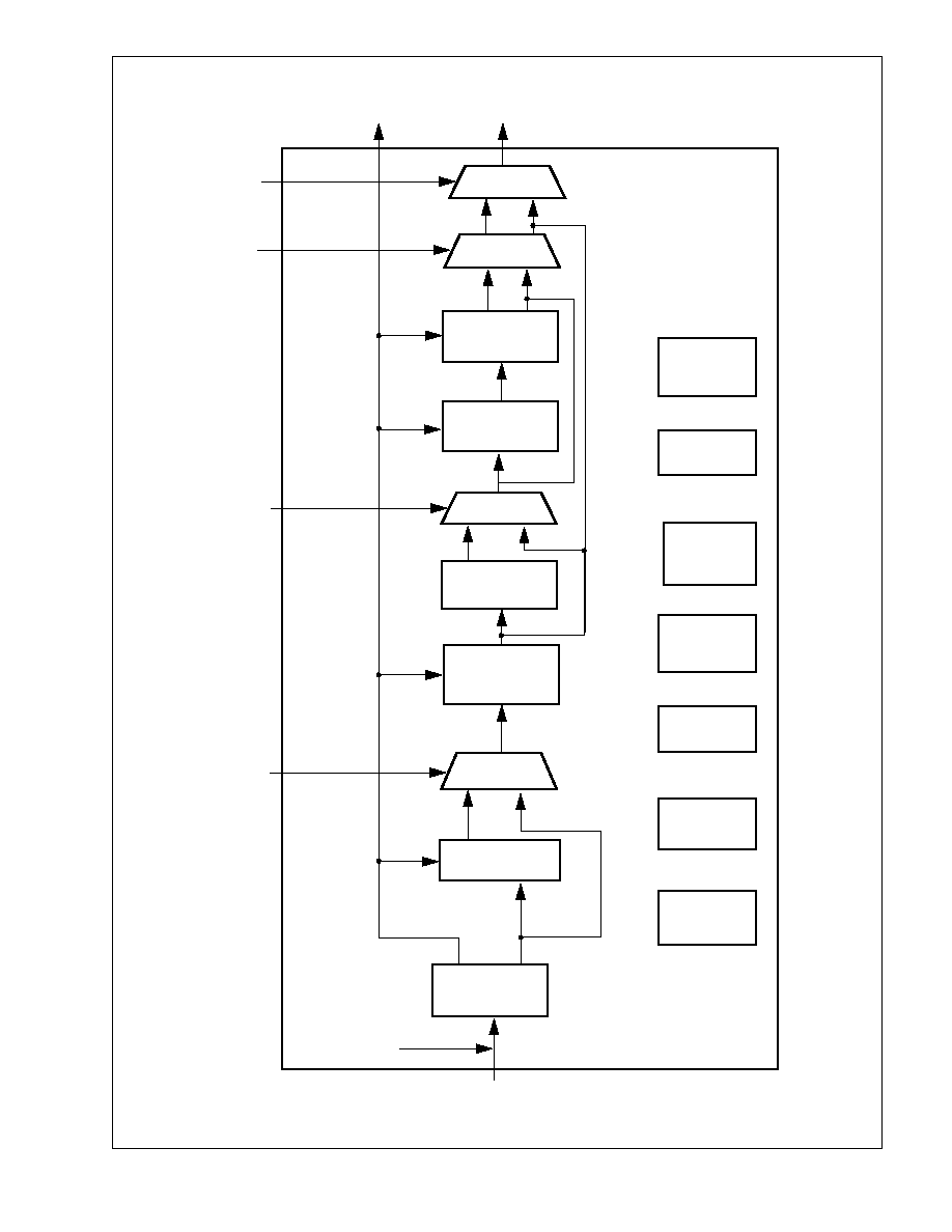
3.4 100BASE-X RECEIVER
The 100BASE-X receiver consists of several functional
blocks which are required to recover and condition the 125
Mb/s receive data stream as specified by the IEEE 802.3u
Standard. The 125 Mb/s receive data stream may originate
from a twisted pair transceiver such as the DP83223
TWISTER in a 100BASE-TX application. Alternatively, the
receive data stream may be generated by an optical
receiver as in a 100BASE-FX application. The block
diagram in Figure 5 provides an overview of each
functional block within the 100BASE-X receive section.
The Receiver block consists of the following functional
blocks:
∑
Clock Recovery block
∑
NRZI to NRZ decoder block (bypass option)
∑
Descrambler block (bypass option)
∑
code-group Alignment block (bypass option)
∑
5B/4B code-group Decoder block (bypass option)
∑
Collision Detect block
∑
Carrier Sense block
∑
100 Mb/s Receive State Machine
∑
Far End Fault Indication block
∑
Link Integrity Monitor block
∑
Carrier Integrity Monitor Block
The bypass option for each of the functional blocks within
the 100BASE-X receiver provides flexibility for applications
such as 100 Mb/s repeaters where data conversion is not
always required.
3.4.1 Clock Recovery
The Clock Recovery Module (CRM) accepts 125 Mb/s
scrambled or unscrambled NRZI data from an external
twisted pair or fiber PMD receiver. The CRM locks onto the
125 Mb/s data stream and extracts a 125 MHz reference
clock. The extracted and synchronized clock and data are
used as required by the synchronous receive operations as
generally depicted in Figure 5.
The CRM is implemented using an advanced digital Phase
Locked Loop (PLL) architecture that replaces sensitive
analog circuits. Using digital PLL circuitry allows the
DP83840A to be manufactured and specified to tighter
tolerances.
3.4.2 NRZI to NRZ
In a typical application the NRZI to NRZ decoder is
required in order to present NRZ formatted data to the
descrambler (or to the code-group alignment block if the
descrambler is bypassed).
The receive data stream, as recovered by the PMD
receiver, is in NRZI format, therefore the data must be
decoded to NRZ before further processing.
3.4.3 Descrambler
A 5-bit parallel (code-group wide) descrambler is used to
de- scramble the receive NRZ data. To reverse the data
scrambling process, the descrambler has to generate an
identical data scrambling sequence (N) in order to recover
the original unscrambled data (UD) from the scrambled
data (SD) as represented in the equations:
Synchronization of the descrambler to the original
scrambling sequence (N) is achieved based on the
knowledge that the incoming scrambled data stream
consists of scrambled IDLE data. After the descrambler
has recognized 16 consecutive IDLE code-groups, where
an IDLE code-group in 5B NRZ is equal to five consecutive
ones (11111), it will synchronize to the receive data stream
and generate unscrambled data in the form of unaligned
5B code-groups.
In order to maintain synchronization, the descrambler must
continuously monitor the validity of the unscrambled data
that it generates. To ensure this, a line state monitor and a
hold timer are used to constantly monitor the
synchronization status. Upon synchronization of the
descrambler the hold timer starts a 722
µ
s countdown.
Upon detection of sufficient IDLE code-groups within the
722
µ
s period, the hold timer will reset and begin a new
countdown. This monitoring operation will continue
indefinitely given a properly operating network connection
with good signal integrity. If the line state monitor does not
recognize sufficient unscrambled IDLE code-groups within
the 722
µ
s period, the entire descrambler will be forced out
UD
SD
N
(
)
=
SD
UD
N
(
)
=
3.0 Functional Description
(Continued)
19
National Semiconductor
Version A
DP83840A 10/100 Mb/s Ethernet Physical Layer
CODE-GROUP
ENCODER
SCRAMBLER
NRZ TO NRZI
ENCODER
PARALLEL
TO SERIAL
TD +/-
_NRZI_EN
BYP_SCR
BYP_4B5B
TX_CLK
TXD[3:0]
FROM CGM
BYP_ALIGN
100BASE-X
LOOPBACK
MUX
MUX
MUX
MUX
CARRIER SENSE
COLLISON
DETECTION
FAR END FAULT
INDICATION
100 Mb/s
TX STATE
MACHINE
FIGURE 4. 100BASE-X Transmitter

3.0 Functional Description
(Continued)
20
National Semiconductor
Version A
DP83840A 10/100 Mb/s Ethernet Physical Layer
Table II. 4B5B code-group Encoding/Decoding.
*Control code-groups I, J, K, T and R in data fields will be mapped as invalid codes, together with RX_ER asserted.
**Normally, invalid codes (V) are mapped to 6h on RXD[3:0] with RX_ER asserted. If the CODE_ERR bit in the LBREMR (bit 4, register address 18h) is
set, the invalid codes are mapped to 5h on RXD[3:0] with RX_ER asserted. Refer to section 4.14 for further detail.
Name
PCS 5B Code-group
MII 4B Nibble Code
DATA CODES
0
11110
0000
1
01001
0001
2
10100
0010
3
10101
0011
4
01010
0100
5
01011
0101
6
01110
0110
7
01111
0111
8
10010
1000
9
10011
1001
A
10110
1010
B
10111
1011
C
11010
1100
D
11011
1101
E
11100
1110
F
11101
1111
IDLE AND CONTROL CODES
H
00100
Halt code-group - Error code
I
11111
Inter-Packet Idle - 0000*
J
11000
First Start of Packet - 0101*
K
10001
Second Start of Packet - 0101*
T
01101
First End of Packet - 0000*
R
00111
Second End of Packet - 0000*
INVALID CODES
V
00000
0110 or 0101*
V
00001
0110 or 0101*
V
00010
0110 or 0101*
V
00011
0110 or 0101*
V
00101
0110 or 0101*
V
00110
0110 or 0101*
V
01000
0110 or 0101*
V
01100
0110 or 0101*
V
10000
0110 or 0101*
V
11001
0110 or 0101*
3.0 Functional Description
(Continued)
21
National Semiconductor
Version A
DP83840A 10/100 Mb/s Ethernet Physical Layer
CODE-GROUP
DECODER
CODE-GROUP
ALIGNMENT
DESCRAMBLER
NRZI TO NRZ
DECODER
CLOCK RECOVERY
MODULE
100 Mb/s
RX STATE
MACHINE
RX_DATA VALID
SSD DETECT
CARRIER SENSE
COLLISON
DETECTION
SERIAL
TO
PARALLEL
RX_CLK
RXD[3:0]
BYP_ALIGN
BYP_4B5B
BYP_SCR
NRZI_EN
RD +/-
CLK
DATA
FAR END FAULT
INDICATION
LINK INTEGRITY
MONITOR
CARRIER
INTEGRITY
MONITOR
MUX
MUX
MUX
MUX
100BASE-X
LOOPBACK
FIGURE 5. 100BASE-X Receiver

3.0 Functional Description
(Continued)
22
National Semiconductor
Version A
DP83840A 10/100 Mb/s Ethernet Physical Layer
of the current state of synchronization and reset in order to
re-acquire synchronization.
The value of the time-out for this timer may be modified from
722 s to 2 ms by setting bit 14 of the PCR (address 17h) to
one. The 2 ms option allows applications with Maximum
Transmission Units (packet sizes) larger than IEEE 802.3 to
maintain descrambler synchronization (i.e. Token Ring/
Fast-Ethernet switch/router applications).
Additionally, this timer may be disabled entirely by setting
bit 13 of the PCR (address 17h) to one. The disabling of the
time-out timer is not recommended as this will eventually
result in a lack of synchronization between the transmit
scrambler and the receive descrambler which will corrupt
data.
3.4.4 Code-group Alignment
The code-group alignment module operates on unaligned
5-bit data from the descrambler (or, if the descrambler is
bypassed, directly from the NRZI/NRZ decoder) and
converts it into 5B code-group data (5 bits). code-group
alignment occurs after the J/K code-group pair is detected.
Once the J/K code-group pair (11000 10001) is detected,
subsequent data is aligned on a fixed boundary.
3.4.5 Code-group Decoder
The code-group decoder functions as a look up table that
translates incoming 5B code-groups into 4B nibbles. The
code-group decoder first detects the J/K code-group pair
preceded by IDLE code-groups and replaces the J/K with
MAC preamble. Specifically, the J/K 10-bit code-group pair
is replaced by the nibble pair (0101 0101). All subsequent
5B code-groups are converted to the corresponding 4B
nibbles for the duration of the entire packet. This
conversion ceases upon the detection of the T/R code-
group pair denoting the End of Stream Delimiter (ESD) or
with the reception of a minimum of two IDLE code-groups.
3.4.6 Collision Detect
Half Duplex collision detection for 100 Mb/s follows the
model of 10BASE-T (refer to section 3.7.3). Collision
detection is indicated by the COL pin of the MII whenever
both the transmit and receive functions within the
DP83840A attempt to process packet data simultaneously.
For Full Duplex applications the COL signal is never
asserted.
3.4.7 Carrier Sense
Carrier Sense (CRS) is asserted, as a function of receive
activity, upon the detection of two non-contiguous zeros
occurring within any 10-bit boundary of the receive data
stream. CRS is asserted, as a function of transmit activity
(depending on the mode of operation), whenever the
TX_EN (transmit enable) input to the DP83840A is
asserted.
For 100 Mb/s Half Duplex operation (non-repeater mode),
CRS is asserted during either packet transmission or
reception.
In REPEATER mode (pin 47/bit 12, register address 17h),
CRS is only asserted due to receive activity.
For 100 Mb/s Full Duplex operation, the behavior of CRS
depends on bit 6 of the LBREMR (address 18h). If this bit
is zero, then CRS is asserted only due to receive activity. If
this bit is one, then CRS is asserted only due to transmit
activity. This operation allows flexibility for interfacing a Full
Duplex MAC to the DP83840A.
When the IDLE code-group pair is detected in the receive
data stream, CRS is deasserted. In modes where transmit
activity results in the assertion of CRS, the deassertion of
TX_EN results in the immediate deassertion of CRS.
The carrier sense function is independent of code-group
alignment.
3.4.8 100 Mb/s Receive State Machine
The DP83840A implements the 100BASE-X receive state
machine diagram as given in ANSI/IEEE Standard 802.3u/
D5, Clause 24.
3.4.9 100BASE-X Link Integrity Monitor
The 100BASE-X Link Integrity Monitor function (LIM)
allows the receiver to ensure that reliable data is being
received. Without reliable data reception, the LIM will halt
both transmit and receive operations until such time that a
valid link is detected (i.e. good link.)
If Auto-Negotiation is not enabled, then a valid link will be
indicated once SD+/- is asserted continuously for 500
µ
s.
If Auto-Negotiation is enabled, then Auto-Negotiation will
further qualify a valid link as follows:
The descrambler must receive a minimum of 15 IDLE
code groups for proper link initialization
Auto-Negotiation must determine that the 100BASE-X
function should be enabled.
A valid link may be detected externally by either the LED3
output or by reading bit 2 of the Basic Mode Status
Register (address 01h.)
3.4.10 Bad SSD Detection
A Bad Start of Stream Delimiter (Bad SSD) is an error
condition that occurs in the 100BASE-X receiver if carrier is
detected (CRS asserted) and a valid /J/K/ set of code
groups (SSD) is not received.
If this condition is detected, then the DP83840A will assert
RX_ER and present RXD[3:0] = 1110 to the MII for the
cycles that correspond to received 5B code-groups until at
least two IDLE code groups are detected. In addition, the
False Carrier Event Counter (address 12h) and the RX_ER
Counter (address 15h) will be incremented by one.
Once at least two IDLE code groups are detected, RX_ER
and CRS become de-asserted.
RX_ER becomes RXD[4] in transparent mode (Bypass_
4B5B), such that RXD[4:0]=11110 during a Bad SSD
event.
When bit 12 of the LBREMR is one (Bypass Align mode),
RXD[3:0] and RX_ER/RXD[4] are not modified regardless
of the state of bit 15 of the LBREMR (Bad SSD Enable.)
Disabling the Bad SSD function supports non-IEEE 802.3u
compliant applications.
3.4.11 Far End Fault Indication
Auto-Negotiation provides a mechanism for transferring
information from the Local Station to the Link Partner that a
remote fault has occurred for 100BASE-TX. As Auto-
Negotiation is not currently specified for operation over
fiber, the Far End Fault Indication function (FEFI) provides
this capability for 100BASE-FX applications.

3.0 Functional Description
(Continued)
23
National Semiconductor
Version A
DP83840A 10/100 Mb/s Ethernet Physical Layer
A remote fault is an error in the link that one station can
detect while the other cannot. An example of this is a
disconnected wire at a station's transmitter. This station will
be receiving valid data and detect that the link is good via
the Link Integrity Monitor, but will not be able to detect that
its transmission is not propagating to the other station.
A 100BASE-FX station that detects such a remote fault
may modify its transmitted IDLE stream from all ones to a
group of 84 ones followed by a single zero (i.e. 16 IDLE
code groups followed by a single Data 0 code group.) This
is referred to as the FEFI IDLE pattern.
If the FEFI function has been enabled via bit 8 of the PAR
(address 19h), then the DP83840A will halt all current
operations and transmit the FEFI IDLE pattern when SD+/-
is de-asserted following a good link indication from the Link
Integrity Monitor. Transmission of the FEFI IDLE pattern
will continue until SD+/- is asserted.
If three or more FEFI IDLE patterns are detected by the
DP83840A, then bit 4 of the Basic Mode Status Register
(address 01h) is set to one until read by management.
Additionally, upon detection of Far End Fault, all receive
and transmit MII activity is disabled/ignored.
This function is optional for 100BASE-FX compliance and
should be disabled for 100BASE-TX compliance.
Note: The first FEFI IDLE pattern may contain more than 84 ones as the
pattern may have started during IDLE transmission. Also, the FEFI IDLE
pattern will not cause carrier detection.
3.4.12 Carrier Integrity Monitor
The Carrier Integrity Monitor function (CIM) protects the
repeater from transient conditions that would otherwise
cause spurious transmission due to a faulty link. This
function is required for repeater applications and is not
specified for node applications.
The REPEATER pin (pin # 47) determines the default state
of bit 5 of the PCR (Carrier Integrity Monitor Disable,
address 17h) to automatically enable or disable the CIM
function as required for IEEE 802.3u/D5 compliant
applications. After power-up/hardware reset, software may
enable or disable this function independent of repeater or
node/switch mode.
If the CIM determines that the link is unstable, the
DP83840A will not propagate the received data or control
signaling to the MII and will ignore data transmitted via the
MII. The DP83840A will continue to monitor the receive
stream for valid carrier events.
Detection of an unstable link condition will cause bit 5 of
the PAR (address 19h) to be set to one. This bit is cleared
to zero upon a read operation once a stable link condition
is detected by the CIM. Upon detection of a stable link, the
DP83840A will resume normal operations.
The Disconnect Counter (address 12h) increments each
time the CIM determines that the link is unstable.
3.5 CLOCK GENERATION MODULE
The Clock Generation Module (CGM) within the DP83840A
can be configured for several different applications. This
offers the flexibility of selecting a clocking scheme that is
best suited for a given design.
This section describes the operation of the CGM from both
the device perspective as well as at the system level such
as in an adapter or repeater. A tolerance of no greater than
50ppm is recommended for all external references driving
the CGM.
It is important to note that in order to provide proper device
initialization, even when operating the DP83840A in
100BASE-X only mode, the 10BASE-T sections of the
device must also be provided with a clock upon device
power-up/reset to ensure proper device initialization. This
is taken into consideration in the following subsections.
It is also important to note that the state of the internal
divide-by-two flip-flop, between OSCIN and CLK25M, is
unknown at power-up/reset. Therefore, the phase of
CLK25M relative to that of OSCIN can be either 0 degrees
or 180 degrees.
3.5.1 Single 50 MHz Reference
This option will support 10BASE-T, 100BASE-X, or
combined 10/100.
A 50 MHz oscillator can be used to drive the OSCIN input.
This reference is internally divided by two and then routed
to the CLK25M output pin. By connecting the CLK25M
output directly to the REFIN input pin, the 25 MHz
reference is allowed to drive the 100 Mb/s module. The 50
MHz signal is also divided by 2.5 internally to provide the
20 MHz reference directly to the 10 Mb/s module. This
option is shown in Figure 6.
The 10BASE-T module within the DP83840A will
automatically switch to the 20 MHz reference (sourced by
the internal 2.5 circuit) upon detection of inactivity on the
X1 input pin. When not in use, the X1 input pin should be
pulled-up to V
CC
(4.7 k
pull-up resistor recommended)).
It should be noted that an external 20 MHz reference
driving the X1 input will provide the best over all transmit
jitter performance from the integrated 10BASE-T
transmitter.
3.5.2 50 MHz and 20 MHz References
This option will support 10BASE-T, 100BASE-X, or
combined 10/100.
For improved jitter performance in the 10 Mb/s module, an
external 20 MHz oscillator can be used to drive the X1 pin.
Alternatively, a 20 MHz crystal network can be connected
across pins X1 and X2 to provide the required reference for
the 10 Mb/s module. The 100 Mb/s module must still
receive a 25 MHz reference which can be provided by a 50
MHz oscillator as described in 3.5.1. This option is shown
in Figure 7 (20 MHz oscillator module) and Figure 8 (20
MHz crystal).
3.5.3 25 MHz and 20 MHz References
This option will support 10BASE-T, 100BASE-X, or
combined 10/100.
A 25 MHz reference, either from an oscillator or a system
clock can directly drive the 100 Mb/s module via the REFIN
input.
A separate 20 MHz reference from either an oscillator or a
crystal network must be provided to the X1 and X2 inputs
as described in 3.5.2. This option is shown in Figure 9.
Because the CLK25M output is not used with this clocking
scheme, it is recommended that it be disabled by setting bit
7 of the PCS Configuration Register (PCR address 17h).
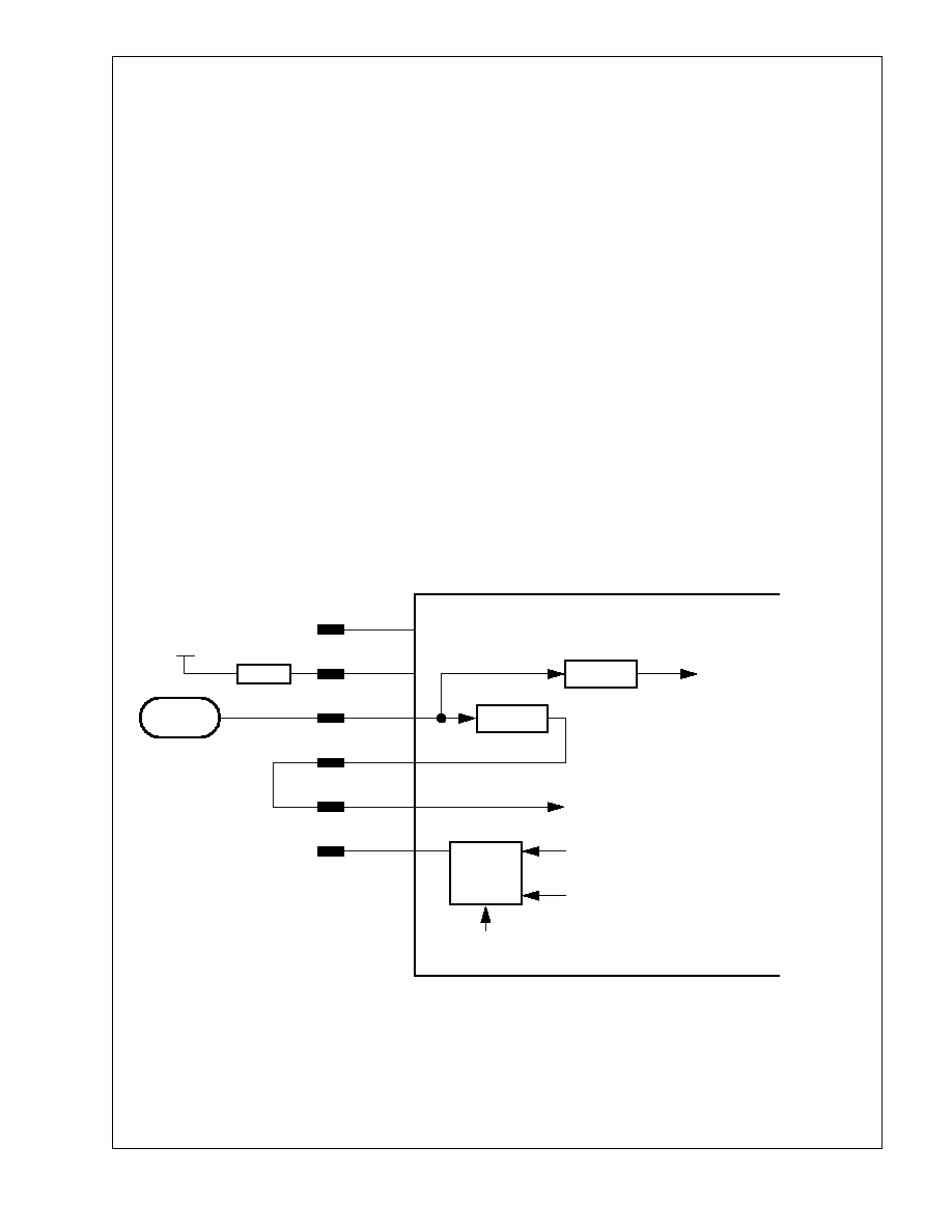
3.0 Functional Description
(Continued)
24
National Semiconductor
Version A
DP83840A 10/100 Mb/s Ethernet Physical Layer
3.5.4 Single 25 MHz Reference
This option will support only 100BASE-X as might be
required in 100BASE-X repeaters that do not employ Auto-
Negotiation. 10BASE-T and Auto-Negotiation will not
function when using this clocking scheme.
A 25 MHz reference, either from an oscillator or a system
clock can directly drive the 100 Mb/s module via the REFIN
input.
The same 25 MHz reference must be also be connected to
the OSCIN input in order to meet the requirement for the
presence of a clock in the 10BASE-T module to ensure
proper device initialization upon power-up/reset. Even
though the divide by 2.5 of the 25MHz clock does not yield
the typical 20MHz 10BASE-T reference, it is still sufficient
for device initialization purposes. This option is shown in
Figure 10.
Because the CLK25M output is not used with this clocking
scheme, it is recommended that it be disabled by setting
bit7 of the PCS Configuration Register (PCR address 17h).
3.5.5 System Clocking
The DP83840A clock options help to simplify single port
adapter designs as well as multi-port repeaters. The
TX_CLK allows 10 Mb/s MII data to be received in either
parallel or serial modes as described in Section 3.1.3. The
standard MII interface clock rate options are as follows:
TX_CLK = 25 MHz for 100 Mb/s nibble mode
TX_CLK = 2.5 MHz for 10 Mb/s nibble mode
Additionally, the DP83840A provides:
TX_CLK = 10 MHz for 10 Mb/s serial mode
3.5.5.1 Adapter Clock Distribution Example
In most single port adapter applications, where only one
DP83840A is required, providing a single 50 MHz oscillator
reference is sufficient for deriving the required MAC and
PHY layer clocks as illustrated in Figure 11. Based on the
50 MHz reference, the DP83840A can generate its own
internal 20 MHz reference for the 10 Mb/s module.
Additionally, the DP83840A can generate the required 25
MHz reference for its 100 Mb/s module.
During 100 Mb/s operation the 25 MHz reference
generated by the DP83840A is available at the TX_CLK
output pin. This can be used for synchronization with the
MAC layer device. During 10 Mb/s operation the TX_CLK
pin sources either a 2.5 MHz or 10 MHz reference to the
MAC layer device. Figure 10 provides an example of the
clock distribution in a typical node design based on the
DP83840A.
FIGURE 6. Single 50 MHz Reference
DIV 2.5
MUX
DIV 2.0
50 MHz
OSC
V
CC
4.7 k
X2
X1
OSCIN
CLK25M
REFIN
TX_CLK
SPEED
SELECT
20 MHz TO 10 Mb/s SECTION
25 MHz TO 100 Mb/s SECTION
25 MHz FROM 100 Mb/s SECTION
2.5 MHz (OR 10 MHz) FROM 10 Mb/s SECTION
50ppm
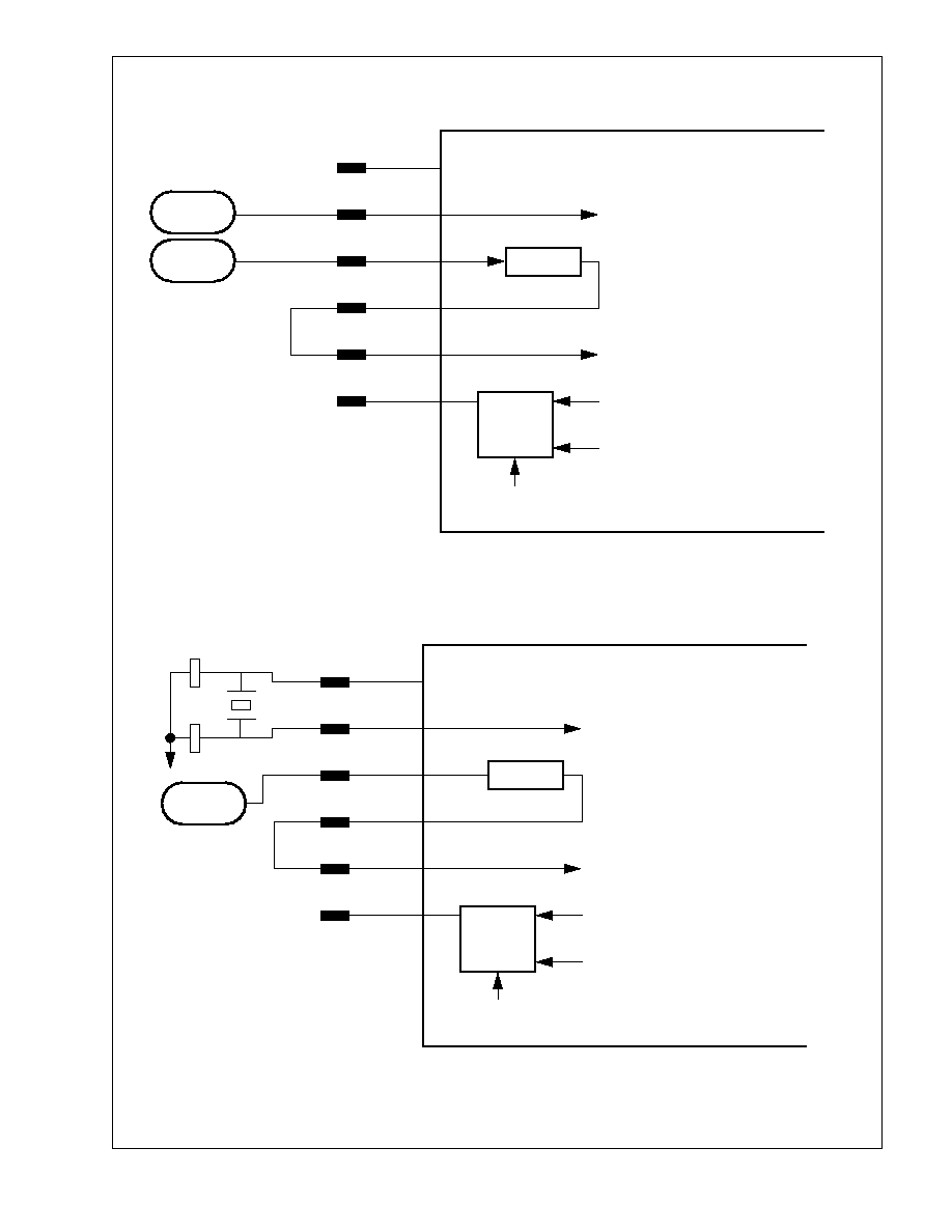
3.0 Functional Description
(Continued)
25
National Semiconductor
Version A
DP83840A 10/100 Mb/s Ethernet Physical Layer
FIGURE 7. 50 MHz and 20 MHz References
MUX
DIV 2.0
50 MHz
OSC
X2
X1
OSCIN
CLK25M
REFIN
TX_CLK
SPEED
SELECT
20 MHz TO 10 Mb/s SECTION
25 MHz TO 100 Mb/s SECTION
25 MHz FROM 100 Mb/s SECTION
2.5 MHz (OR 10 MHz) FROM 10 Mb/s SECTION
50ppm
20 MHz
OSC
50ppm
MUX
DIV 2.0
50 MHz
OSC
X2
X1
OSCIN
CLK25M
REFIN
TX_CLK
SPEED
SELECT
20 MHz TO 10 Mb/s SECTION
25 MHz TO 100 Mb/s SECTION
25 MHz FROM 100 Mb/s SECTION
2.5 MHz (OR 10 MHz) FROM 10 Mb/s SECTION
50ppm
20 MHZ
0.005%
* 33 pF
* 33 pF
* NOTE:
REFER TO CRYSTAL MANUFACTURE FOR RECOMMENDED CRYSTAL LOAD CAPACITANCE
FIGURE 8. 50 MHz Reference and 20 MHz Crystal
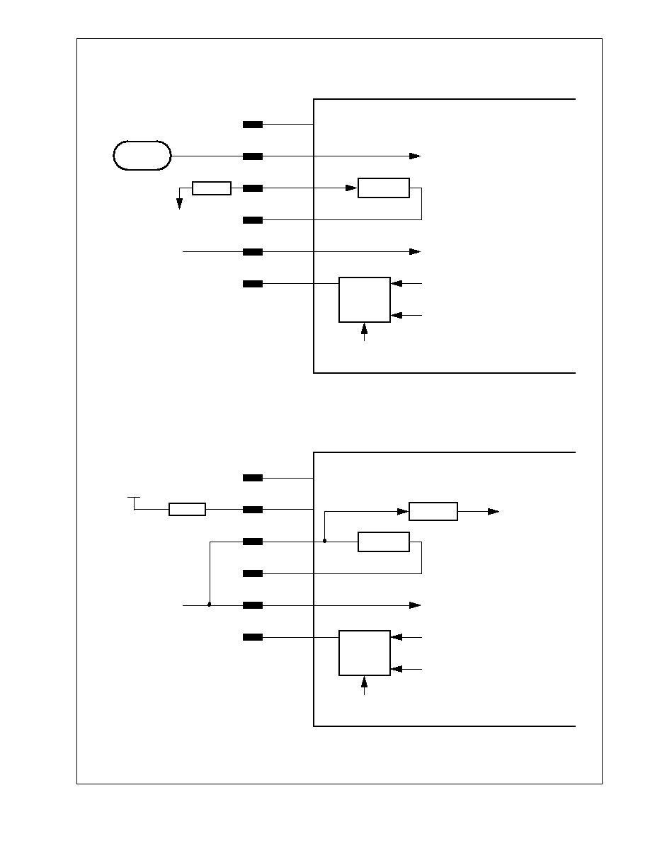
3.0 Functional Description
(Continued)
26
National Semiconductor
Version A
DP83840A 10/100 Mb/s Ethernet Physical Layer
FIGURE 9. 25 MHz and 20 MHz References
MUX
DIV 2.0
20 MHz
OSC
4.7 k
X2
X1
OSCIN
CLK25M
REFIN
TX_CLK
SPEED
SELECT
20 MHz TO 10 Mb/s SECTION
25 MHz TO 100 Mb/s SECTION
25 MHz FROM 100 Mb/s SECTION
2.5 MHz (OR 10 MHz) FROM 10 Mb/s SECTION
50ppm
25 MHz SYSTEM
REFERENCE
50ppm
FROM 10 Mb/s SECTION
MUX
DIV 2.0
X2
X1
OSCIN
CLK25M
REFIN
TX_CLK
SPEED
SELECT
25 MHz TO 100 Mb/s SECTION
25 MHz FROM 100 Mb/s SECTION
25 MHz SYSTEM
REFERENCE
50ppm
V
CC
4.7 k
DIV 2.5
TO 10 Mb/s SECTION
FIGURE 10. Single 25 MHz Reference
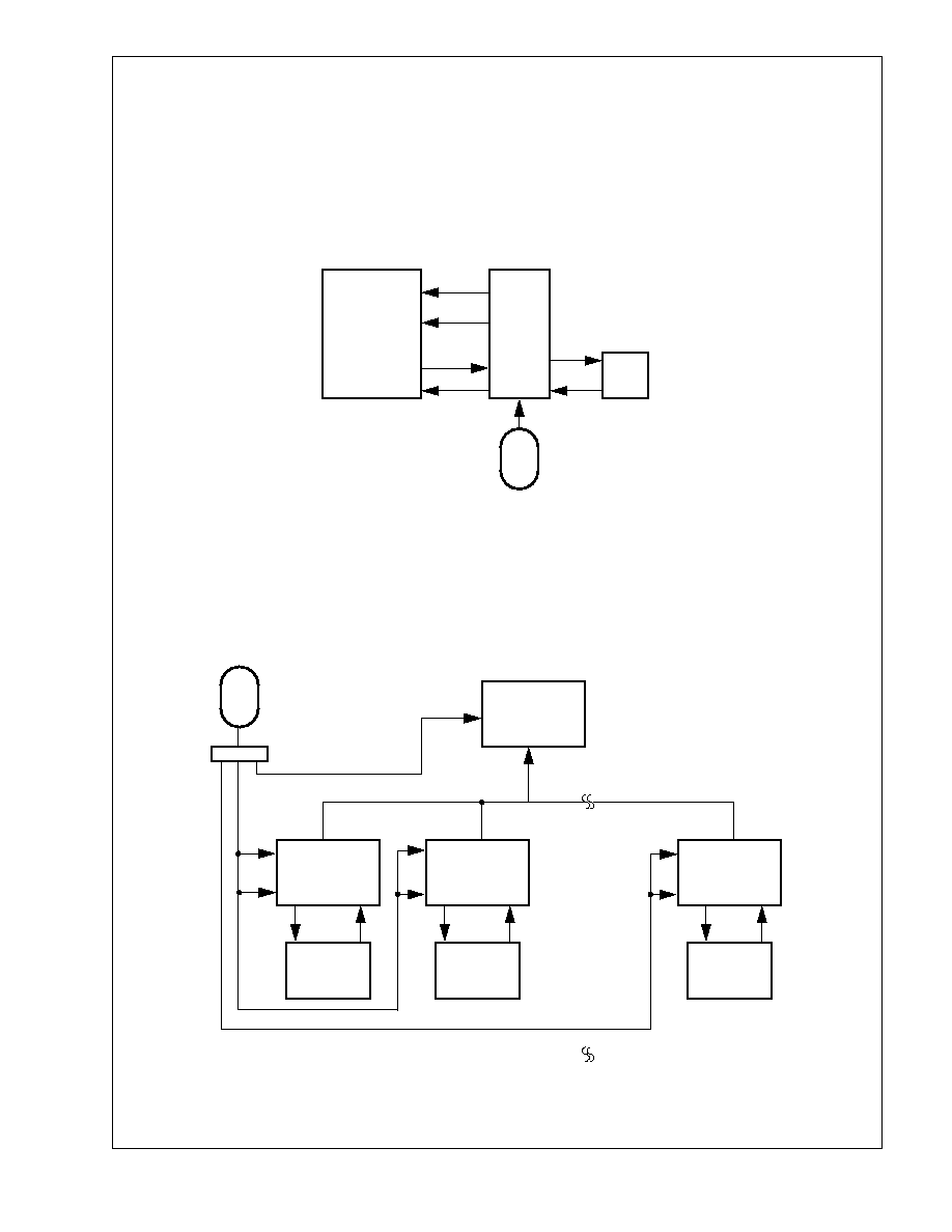
3.0 Functional Description
(Continued)
27
National Semiconductor
Version A
DP83840A 10/100 Mb/s Ethernet Physical Layer
3.5.5.2 Repeater Clock Distribution Example
The clock distribution within a multi-port repeater can be
designed in a variety of ways. Figure 12 provides a
simplified example of one possible timing distribution
scheme in a 100 Mb/s only repeater design. It should be
noted that in order to support Auto-Negotiation, a 20 MHz
reference would be required for each DP83840A device.
ENDEC
(DP83850
100RIC)
DP83840A (1)
DP83840A (2)
DP83840A (12)
DP83223
(1)
DP83223
(2)
DP83223
(12)
25 MHz
25
MHz
BUFFER
RX_CLK
MAC
PHY
PMD
RXD
TX_CLK
RX_CLK
TXD
TD
RD
50
MHz
FIGURE 12. Typical 100 Mb/s Repeater Clock Interconnection
FIGURE 11. Typical Adapter Clock and Data Typical
Due to the demanding timing constraints required to
maintain standards compliance, great care must be
taken in the design and layout of a multi-port repeater
system. The example provided in Figure 12 illustrates
interconnection only and should not be considered as a
reference design.

3.0 Functional Description
(Continued)
28
National Semiconductor
Version A
DP83840A 10/100 Mb/s Ethernet Physical Layer
3.6 CLOCK RECOVERY MODULE
The Clock Recovery Module (CRM) is part of the 100 Mb/s
receive channel. The 10 Mb/s clock recovery is
independent from the CRM.
The CRM contains a Phase Locked Loop that tracks the
signal frequency of the incoming 125 Mb/s data stream at
the RD+/- inputs. The CRM extracts a synchronous 125
MHz clock from this data (the data rate on the cable is 125
Mb/s due to 4B5B encoding). The CRM obtains its initial
frequency and stability from its own internal VCO and then
adjusts the frequency as required to match the incoming
data stream frequency. The CRM maintains control of the
PLL's loop gain to minimize the lock time as well as to
minimize the jitter after phase lock has been acquired.
When the Signal Detect (SD+/-) inputs become active, the
CRM attempts to acquire lock. Upon the deassertion of
Signal Detect, the CRM remains locked to the frequency of
the most recent datastream that it had locked to prior to SD
deassertion.
The CRM generates a 125 MHz clock synchronous with
the receive data stream and presents both the clock and
data to the rest of the 100 Mb/s receive section. The CRM
is not synchronous with the local clock present at the
REFIN input to the CGM.
The RX_CLK signal at the MII interface is derived from the
CRM 125 Mb/s clock during 100 Mb/s operation. The
RX_CLK frequency is set to 25 MHz for nibble-wide receive
data passing to the MAC and/or Repeater.
3.7 10BASE-T TRANSCEIVER MODULE
The 10BASE-T Transceiver Module is IEEE 802.3
compliant. It includes the receiver, transmitter, collision,
heartbeat, loopback, jabber, and link integrity functions, as
defined in the standard. An external filter is not required on
the 10BASE-T interface since this is integrated inside the
DP83840A. Figure 13 provides a detailed block level
representation of the complete 10BASE-T transceiver
within the DP83840A. Due to the complexity and scope of
the 10BASE-T Transceiver block and various sub-blocks,
this section focuses on the general system level operation.
3.7.1 Operational Modes
The DP83840A has 2 basic 10 Mb/s operational modes:
∑
Half Duplex mode
∑
Full Duplex mode
3.7.1.1 Half Duplex Mode
In Half Duplex mode the DP83840A functions as a
standard IEEE 802.3 10BASE-T transceiver with fully
integrated filtering for both the transmit and receive
10BASE-T signaling (refer to section 3.7).
3.7.1.2 Full Duplex Mode
In Full Duplex mode the DP83840A is capable of
simultaneously transmitting and receiving without asserting
the collision signal. The DP83840A's 10 Mb/s ENDEC is
designed to encode and decode simultaneously.
3.7.2 Oscillator Module Operation
A 20MHz crystal or can-oscillator with the following specifi-
cations is recommended for driving the X1 input.
1.TTL or CMOS output with a 50ppm frequency tolerance
2. 40-60% duty cycle (max).
3.Two TTL load output drive
The circuit is shown in Figure 15. Additional output drive
may be necessary if the oscillator must also drive other
components. When using a clock oscillator it is still
recommended that the designer connect the oscillator
output to the X1(OSCIN) pin and leave X2(OSCOUT)
floating
3.7.3 Smart Squelch
The Smart Squelch is responsible for determining when
valid data is present on the differential receive inputs (RXI).
The DP83840A implements an intelligent receive squelch
on the RXI differential inputs to ensure that impulse noise
on the receive inputs will not be mistaken for a valid signal.
Smart squelch operation is independent of the 10BASE-T
operational mode.
The squelch circuitry employs a combination of amplitude
and timing measurements (as specified in the IEEE 802.3
10BASE-T standard) to determine the validity of data on
the twisted pair inputs (refer to figure 14).
The signal at the start of packet is checked by the smart
squelch and any pulses not exceeding the squelch level
(either positive or negative, depending upon polarity) will
be rejected. Once this first squelch level is overcome cor-
rectly the opposite squelch level must then be exceeded
within 150ns. Finally the signal must exceed the original
squelch level within a further 150ns to ensure that the input
waveform will not be rejected. The checking procedure
results in the loss of typically three bits at the beginning of
each packet.
Only after all these conditions have been satisfied will a
control signal be generated to indicate to the remainder of
the circuitry that valid data is present. At this time, the
smart squelch circuitry is reset.
Valid data is considered to be present until squelch level
has not been generated for a time longer than 150ns,
indicating End of Packet. Once good data has been
detected the squelch levels are reduced to minimize the
effect of noise causing premature End of Packet detection.
The receive squelch threshold level can be lowered for use
in longer cable or STP applications. This is achieved by
setting the LSS bit in the 10BTCR (bit 2, register address
1Ch).
3.7.4 Collision Detection
For Half Duplex, a 10BASE-T collision is detected when
the receive and transmit channels are active
simultaneously. Collisions are reported by the COL signal
on the MII.
If the ENDEC is transmitting when a collision is detected,
the collision is not reported until seven bits have been
received while in the collision state. This prevents a
collision being reported incorrectly due to noise on the
network. The COL signal remains set for the duration of the
collision.
When heartbeat is enabled, approximately 1
µ
s after the
transmission of each packet, a Signal Quality Error (SQE)
signal of approximately 10 bit times is generated
(internally) to indicate successful transmission. SQE is
reported as a pulse on the COL signal of the MII.
3.7.5 Carrier Sense
Carrier Sense (CRS) may be asserted due to receive
activity once valid data is detected via the Smart Squelch
function.
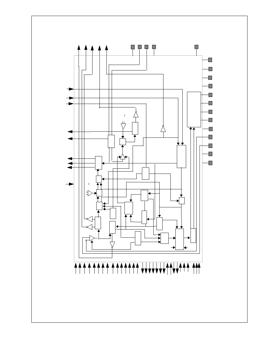
3.0 Functional Description
(Continued)
29
National Semiconductor
Version A
DP83840A 10/100 Mb/s Ethernet Physical Layer
mux
mux
mux
mux
Smart squelch
link detector
XWRAP
jabber
collision decoder
.
.
.
.
.
.
.
RXVCC
RXGND
RXI_MINUS
RXI_PLUS
TDVCC
TXS_MINUS
TXS_PLUS
TXU_MINUS
TXU_PLUS
TDGND
prescaler
.
generator
link
RT
X
REQ
.
PLL
VCC
TPI Output Dri
v
e
r
Xmit filter
pre-emphasis
TD dri
v
e
r
timer
Heartbeat
TFI
control
mux
.
.
CD
+
COL
TXC
CRS
RXD
RXC
decoder
PLL
TXD
TXE
O
VCC
X1
X2
OGND
TXLEDB
RXLEDB
COLLEDB
POLLEDB
LNKLEDB
RESET
RX
+
oscillator
XT
AL
TX
logic
control
LBK
control
TPI RXI
+
RTX
REQ
PLLGND
data control
Encoder &
Manchester
LOOPBACK
FIGURE 13. 10BASE-T Transceiver Block Diagram
RX_FIL
T
TPITEST
INIT
RDPTHB
J
ABDISB
HR
TDS
XMT
UTP_STP
TX_FIL
T
LOCK*
FREEZE10BT*
V_IBIAS*
GA
TE_RXC*
LINKPULSE*
V
O
L
T_SEL
EWRAP
TENRST
TRES
A
U
T
OSB
TEST
TFI
XWRAP
LNKDISB
HBE
LO
WSQL
A
UITP
J
ABEN
TPTST
TPI_EN*
TX_FLP*
L
TPR
EN

3.0 Functional Description
(Continued)
30
National Semiconductor
Version A
DP83840A 10/100 Mb/s Ethernet Physical Layer
For 10 Mb/s Half Duplex operation, CRS is asserted during
either packet transmission or reception.
For 10 Mb/s Full Duplex operation, the behavior of CRS
depends on bit 6 of the LBREMR (address 18h). If this bit
is zero, then CRS is asserted only due to receive activity. If
this bit is one, then CRS is asserted only due to transmit
activity. This operation allows flexibility for interfacing a Full
Duplex MAC to the DP83840A.
CRS is deasserted following an end of packet.
In REPEATER mode (pin 47/bit 12, register address 17h),
CRS is only asserted due to receive activity.
3.7.6 Normal Link Pulse Detection/Generation
The link pulse generator produces pulses as defined in the
IEEE 802.3 10BASE-T standard. Each link pulse is
nominally 100 ns in duration and is transmitted every 16
ms 8ms, in the absence of transmit data.
Link pulse is used to check the integrity of the connection
with the remote end. If valid link pulses are not received,
the link detector disables the 10BASE-T twisted pair
transmitter, receiver and collision detection functions.
When the link integrity function is disabled, the 10BASE-T
transceiver will operate regardless of the presence of link
pulses.
In 10 Mb/s ENDEC loopback mode (bit 11, register
address 18h), transmission and reception paths can be
tested regardless of the incoming link status.
3.7.7 Jabber Function
The Jabber function monitors the DP83840A's output and
disables the transmitter if it attempts to transmit a longer
than legal sized packet. A jabber timer monitors the
transmitter and disables the transmission if the transmitter
is active for greater than approximately 26ms.
Once disabled by the Jabber function, the transmitter stays
disabled for the entire time that the ENDEC module's
internal transmit enable is asserted. This signal has to be
de-asserted for approximately 750ms (the "unjab" time)
before the Jabber function re-enables the transmit outputs.
The Jabber function is only meaningful in 10BASE-T mode.
3.7.8 Transmit Outputs
There are two pairs of 10BASE-T output signals. One pair
for Unshielded cable (TXU+/-) and one pair for Shielded
cable (TXS+/-). These two sets of differential outputs are
actually identical to one another. They are both included in
the DP83840A for increased flexibility in multiple media
designs. Note that the characteristic differential cable
impedance for Unshielded cable is 100 Ohms (nominally)
and for Shielded cable is 150 ohms (nominally). Therefore,
special attention must be paid to the external termination
resistor values in order to properly match the 10BASE-T
driver impedance to the load. Refer to Figure 15 for further
detail.
Selection between 100 UTP and 150 STP cable operation
is accomplished using the UTP/STP bit in the 10BASE-T
Configuration Register (bit 3, register address 1Ch). Only
one set of outputs is active at any given time. Selecting
UTP will TRI-STATE STP and vice versa.
The TXU+/- and TXS+/- outputs of the DP83840A are
internally filtered and require no additional external
filtering. See Section 3.7.12 for further detail.
During 100 Mb/s operation, both the TXU+/- and TXS+/-
outputs are tri-stated.
3.7.9 Status Information
10BASE-T Status Information is available on the LED
output pins of the DP83840A. Transmit activity, receive
activity, link status, link polarity and collision activity
information is output to the five LED output pins (LED1 to
LED5). See Section 2.6 for more information on these
outputs.
If required the LED outputs can be used to provide digital
status information to external circuitry.
The Link LED output (LED3, pin #38) indicates Good Link
status for both 10 and 100 Mb/s modes. In Half Duplex
10BASE-T mode, LED3 indicates link status.
The link integrity function can be disabled. When disabled,
the transceiver will operate regardless of the presence of
link pulses and the Link LED will stay lit continuously.
3.7.10 Automatic Link Polarity Detection
The DP83840A's 10BASE-T Transceiver Module
incorporates an automatic link polarity detection circuit.
When seven consecutive link pulses or three consecutive
receive packets with inverted End-of-Packet pulses are
received, bad polarity is reported.
A polarity reversal can be caused by a wiring error at either
end of the UTP/STP cable, usually at the Main Distribution
Frame (MDF) or patch panel in the wiring closet.
The bad polarity condition is latched and the LED4 output
is asserted. The DP83840A's 10BASE-T Transceiver
Module corrects for this error internally and will continue to
decode received data correctly. This eliminates the need to
correct the wiring error immediately.
3.7.11 10BASE-T Internal Loopback
When the 10BT_LPBK bit in the LBREMR (bit 11, register
address 18h) is set, 10BASE-T transmit data is looped
back in the ENDEC to the receive channel. The transmit
drivers and receive input circuitry are disabled in
transceiver loopback mode, isolating the transceiver from
the network.
Loopback is used for diagnostic testing of the data path
through the transceiver without transmitting on the network
or being interrupted by receive traffic. This loopback
function causes the data to loopback just prior to the
10BASE-T output driver buffers such that the entire
transceiver path is tested.
3.7.12 Transmit and Receive Filtering
External 10BASE-T filters are not required when using the
DP83840A as the required signal conditioning is
integrated.
Only isolation/step-up transformers and impedance
matching resistors are required for the 10BASE-T transmit
and receive interface. The internal transmit filtering
ensures that all the harmonics in the transmit signal are
attenuated by at least 30 dB.
3.7.13 Encoder/Decoder (ENDEC) Module
The Endec Module consists of essentially four functions:
The oscillator generates the 10 MHz transmit clock signal
for system timing from a 20 MHz oscillator.
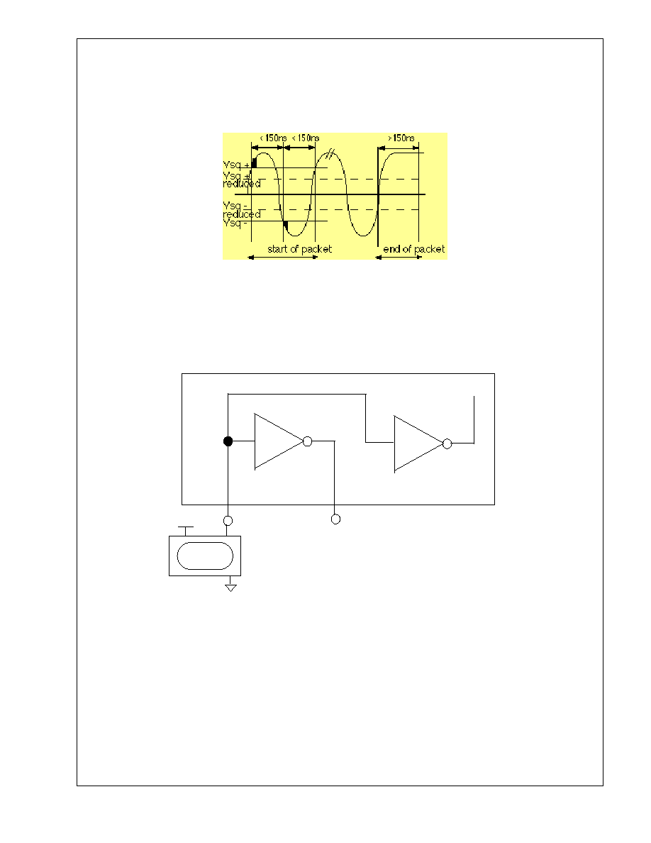
3.0 Functional Description
(Continued)
31
National Semiconductor
Version A
DP83840A 10/100 Mb/s Ethernet Physical Layer
Twisted Pair Squelch Operation
FIGURE 14. 10BASE-T Twisted Pair Smart Squelch Operation
20 MHz
(50ppm)
(OSCIN)
(OSCOUT)
X1
X2
Alternatively, a 20MHz crystal (with nominal 12pF loading)
can be utilized in place of the oscillator. When not used, X1 should
be pulled-up to Vcc (4.7k
recommended).
FIGURE 15. X1 and X2 Oscillator Module
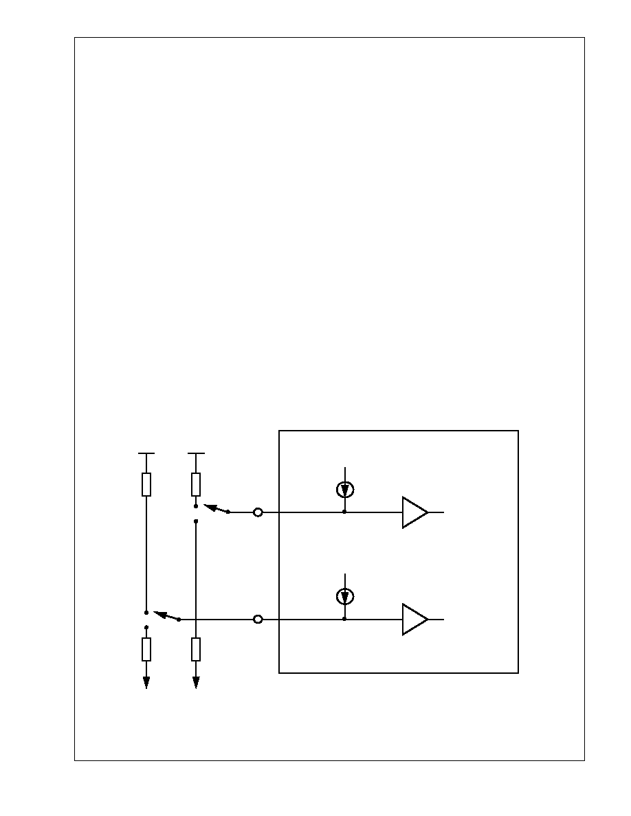
3.0 Functional Description
(Continued)
32
National Semiconductor
Version A
DP83840A 10/100 Mb/s Ethernet Physical Layer
The Manchester encoder accepts NRZ data from the
controller or repeater, encodes the data to Manchester,
and transmits it differentially to the transceiver, through the
differential transmit driver.
The Manchester decoder receives Manchester data from
the transceiver, converts it to NRZ data and recovers clock
pulses for synchronous data transfer to the controller or
repeater.
The collision monitor indicates to the controller the
presence of a valid 10 MHz collision signal.
3.7.13.1 Manchester Encoder and differential driver
The encoder begins operation when the Transmit Enable
input (TX_EN) goes high and converts the NRZ data to
pre-emphasized Manchester data for the transceiver. For
the duration of TXE remaining high, the Transmit Data
(TXD) is encoded for the transmit-driver pair (TXU+/- or
TXS+/-). TXD must be valid on the rising edge of Transmit
Clock (TXC). Transmission ends when TX_EN deasserts.
The last transition is always positive; it occurs at the center
of the bit cell if the last bit is a one, or at the end of the bit
cell if the last bit is a zero.
3.7.13.2 Manchester Decoder
The decoder consists of a differential receiver and a PLL to
separate a Manchester encoded data stream into internal
clock signals and data. The differential input must be
externally terminated with either a differential 100
or
differential 150
termination network to accommodate
either UTP or STP cable respectively. Refer to Figure 16
for further detail.
The decoder detects the end of a frame when no more
mid-bit transitions are detected. Within one and a half bit
times after the last bit, carrier sense is de-asserted.
Receive clock stays active for five more bit times after CRS
goes low, to guarantee the receive timings of the controller
or repeater.
3.7.14 REQ and RTX
These pins allow for the direct control of both the pre-
emphasis (REQ) and the transmit amplitude (RTX) of the
10BASE-T transmit signal. These pins should normally be
left floating, however, in applications where lower transmit
amplitudes are required, these pins should be pulled-down
to ground resistively. Conversely, for applications that
require higher transmit amplitudes, these pins should be
pulled-up to Vcc resistively. Figure 16 provides a simplified
functional diagram.
Some experimentation is required in order to fully evaluate
the extent of transmit amplitude (and corresponding pre-
emphasis) variation due to the system to system variations
in external components (e.g. transformers and termination
networks). It is important to use the same resistor value for
both RTX and REQ (pulled to the same rail) in order to
allow the pre-emphasis to track the transmit amplitude.
In general terms, a value of approximately 50K
for these
pins (either pulled-up or pulled-down) will result in a
transmit amplitude (and pre-emphasis) change on the
order of 5% to 10%. Again, experimentation is
recommended.
RTX
REQ
Transmit
Amplitude
Control
Transmit
Pre-emphasis
Control
Fixed
Current
Source
Fixed
Current
Source
GND
Vcc
R
R
R
R
FIGURE 16. REQ and RTX Operation
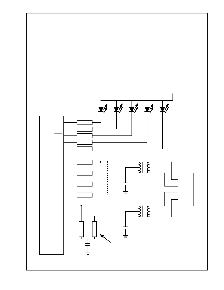
3.0 Functional Description
(Continued)
33
National Semiconductor
Version A
DP83840A 10/100 Mb/s Ethernet Physical Layer
3.7.15 Typical Node Application
An example of the 10BASE-T interface is shown in Figure
17. The TXS+/- signals are used for STP and the TXU+/-
signals for UTP. Standard UTP applications do not require
connection of the TXS+/- outputs. The output resistor
values are chosen to match the transmit output impedance
to the impedance of the twisted pair cable.
The DP83840A 10BASE-T outputs require a 1:2 step-up
isolation transformer in order to match the cable
impedance. The 10BASE-T inputs require a 1:1 isolation
transformer and appropriate line termination. Refer to
Figure 16.
3.8 IEEE 1149.1 CONTROLLER
The IEEE 1149.1 standard defines a test access port and
boundary-scan architecture for digital integrated circuits
and for the digital portions of mixed analog/digital
integrated circuits. Figure 18 depicts the IEEE 1149.1
architecture.
The standard provides a solution for testing assembled
printed circuit boards and other products based on highly
complex digital integrated circuits and high-density surface-
mounting assembly techniques. It also provides a means of
accessing and controlling design-for-test features built into
the digital integrated circuits. Such features include internal
scan paths and self-test functions as well as other features
intended to support service applications in the assembled
DP83840A
LED1
LED2
RXI-
RXI+
TXS-
TXS+
LED3
LED4
LED5
TXU+
TXU-
TRANSMIT
RECEIVE
LINK
COLLISION
POLARITY/FULL DUPLEX
V
CC
LOW CURRENT LEDS
1:2
10.5
1%
10.5
1%
16.5
1%
16.5
1%
0.01
µ
F
1:1
0.01
µ
F
TD-
TD+
RD-
RD+
10BASE-T
INTERFACE
RJ45
0.01
µ
F
49.9
1%
49.9
1%
Note: Resistors from TXS + / - outputs can
1.5K
5%
1.5K
5%
1.5K
5%
1.5K
5%
1.5K
5%
be added if STP cable support is required.
(For STP applications, the RXI+/- termination
resistors should each be 75
+/-1%)
FIGURE 17. Typical 10BASE-T Node Application

3.0 Functional Description
(Continued)
34
National Semiconductor
Version A
DP83840A 10/100 Mb/s Ethernet Physical Layer
product. The IEEE 1149.1 Boundary Scan Architecture
document should be referenced for additional detail.
The circuitry defined by this standard allows test
instructions and associated data to be input serially into a
device. The instruction execution results are output serially.
The DP83840A reserves five pins, called the Test Access
Port (TAP), to provide test access: TMS, TCK, Test Data
Input (TDI), Test Data Output (TDO) and Test Reset
(TRST). These signals are described in Section 2.7. To
ensure race-free operation all input and output data is
synchronous to the test clock (TCK). TAP input signals
(TMS and TDI) are clocked into the test logic on the rising
edge of TCK while output signal (TDO) is clocked on the
falling edge.
3.8.1 Test Logic
The IEEE 1149.1 Test Logic consists of a Test Access Port
(TAP) controller, an instruction register, and a group of test
data registers including Bypass, Device Identification and
Boundary Scan registers.
The TAP controller is a synchronous 16 state machine that
responds to changes at the TMS and TCK signals.
This controls the sequence of operations by generating
clock and control signals to the instruction and test data
registers. The control signals switch TDI and TDO between
instruction and test data registers.
The DP83840A implements 4 basic instructions: ID_Code,
bypass, Sample/Preload and Extest. Upon reset, the
ID_Code instruction is selected by default. If the ID_Code
instruction is not supported, the bypass instruction is
selected instead.
3.8.1.1 ID_Code Instruction
The ID_Code instruction allows users to select the 32-bit
IDCODE register and interrogate the contents which
consist of the manufacturer's ID, part ID and the version
number.
3.8.1.2 Bypass Instruction
The bypass instruction uses the bypass register. The
bypass register contains a single shift-register stage and is
used to provide a minimum length serial path between the
TDI and TDO pins of the DP83840A when test operation is
not required. This allows more rapid movement of test data
to and from other testable devices in the system.
3.8.1.3 Sample/Preload Instruction
The Sample/Preload instruction allows scanning of the
boundary-scan register without causing interference to the
normal operation of the on-chip system logic.
Two functions are performed when this instruction is
selected.
Sample allows a snapshot to be taken of the data flowing
from the system pins to the on-chip test logic or vice versa,
without interfering with normal operation. The snapshot is
taken on the rising edge of TCK in the Capture-DR
controller state, and the data can be viewed by shifting
through the component's TDO output.
While sampling and shifting data out through TDO for
observation, preload allows an initial data pattern to be
shifted in through TDI and to be placed at the latched
parallel output of the boundary-scan register cells which
are connected to system output pins. This ensures that
known data is driven through the system output pins upon
entering the Extest instruction.
Without Preload, indeterminate data would be driven until
the first scan sequence has been completed. The shifting
of data for the Sample and Preload phases can occur
simultaneously. While data capture is being shifted out, the
preload data can be shifted in.
3.8.1.4 Extest Instruction
The Extest instruction allows circuitry external to the
DP83840A (typically the board interconnections) to be
tested.
Prior to executing the Extest instruction, the first test
stimulus to be applied will be shifted into the boundary-
scan registers using the Sample/Preload instruction. Thus,
when the change to the Extest instruction takes place,
known data will be driven immediately from the DP83840A
to its external connections.
This provides stimulus to the system input pins of adjacent
devices on the assembled printed circuit boards. Figure 14
below illustrates the IEEE 1149.1 architecture.
3.8.2 Device Testing
IEEE 1149.1 provides a simple solution for testing many of
the standard static pin parametrics. Reasonably accurate
limits may be tested as a functional pattern.
The IEEE 1149.1 test circuitry is tested itself as a
consequence of testing pin parametrics. Specific tests are:
TRI-STATE conditions of TDO when serial shift
between TDI and TDO is not selected
Input leakage of TCK, TMS, TDI and TRST
Output has TRI-STATE leakage of TDO
Opens and shorts of TCK, TMS, TDI, TRST, and TDO
IDCODE register, the bypass register and the TAP
controller state machine sequences
Open and shorted pins can be identified by placing an
alternating bit pattern
on the I/O pins. Any shorted bond wires would either cause
an input to be misinterpreted in the inputs scan phase, or
the test comparator would fail an output during data scan.
Repeating the test with the inverse bit pattern provides
coverage of V
CC
and GND short/open circuits.
3.8.3 Boundary Scan Description Language File
A Boundary Scan Description Language (BSDL) file is
available. Contact your local National Semiconductor
representative to obtain the latest version.
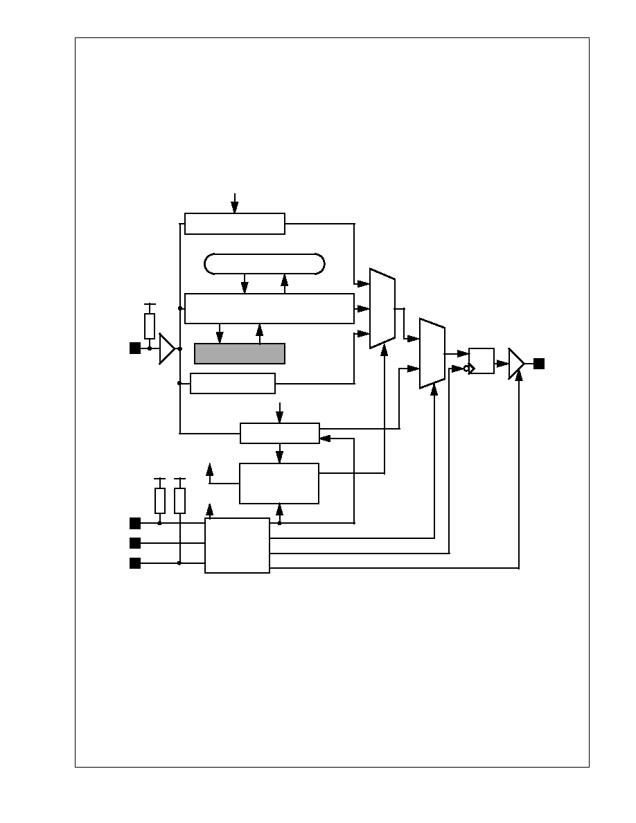
3.0 Functional Description
(Continued)
35
National Semiconductor
Version A
DP83840A 10/100 Mb/s Ethernet Physical Layer
TDI
MANUFACTURER CODE
CORE LOGIC
PAD LOGIC
BOUNDARY SCAN REGISTER
(CELLS ARE ANY ONE OF BC1 THRU BC6)
BYPASS REGISTER
DATA
MUX
DI
MUX
TDO
TDO DRIVER
DATA
REGISTER
SELECT
GATED DR-CLOCK AND MODE SIGNALS
INSTR. REGISTER
INSTR. REGISTER
AND
DR CLOCK GATING
LOGIC
INSTR. PRELOAD
DR-CLOCKS
IR-CLOCKS
TAP
CONTROLER
RESET
TMS
TCK
TRST
SELECT
ENABLE
~TCK
IDCODE REGISTER
FIGURE 18. TIEEE 1149.1 Architecture
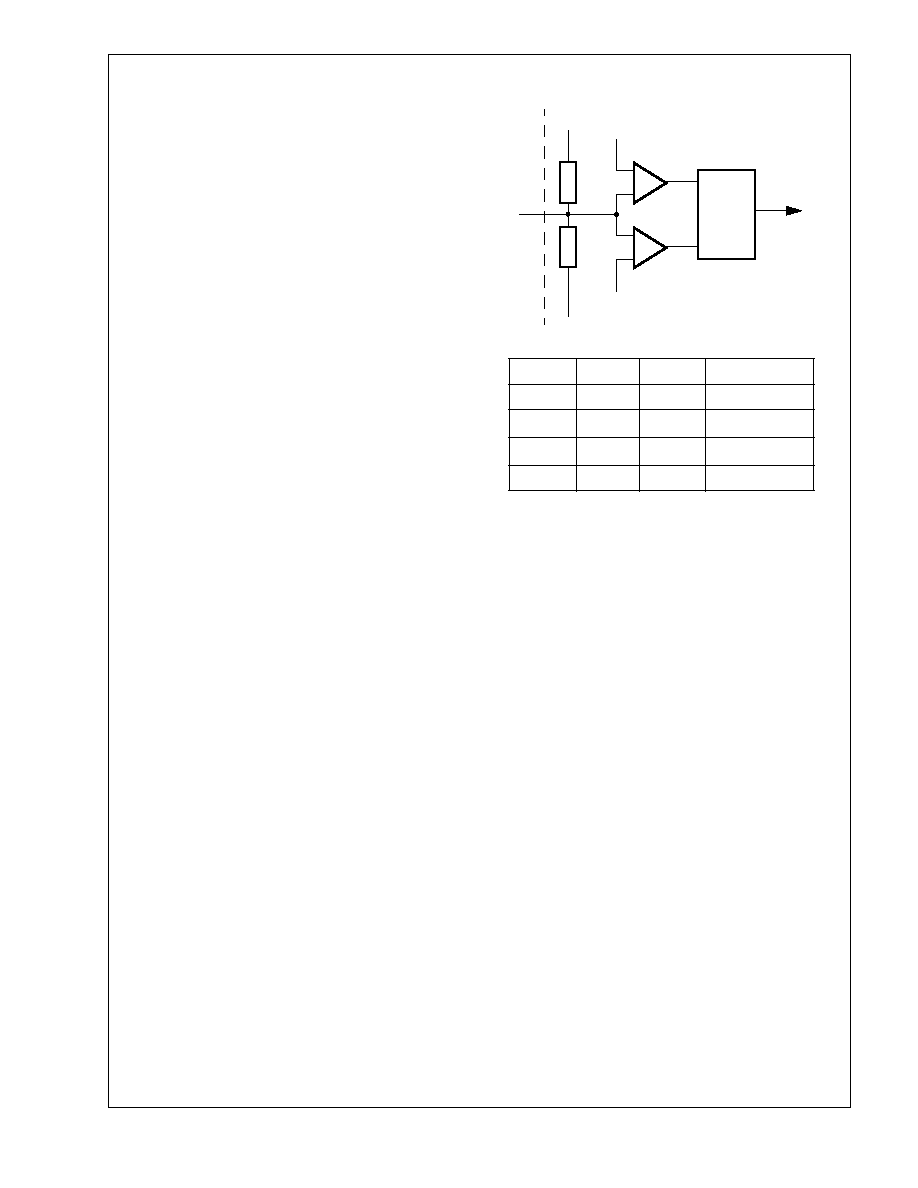
3.0 Functional Description
(Continued)
36
National Semiconductor
Version A
DP83840A 10/100 Mb/s Ethernet Physical Layer
3.9 IEEE 802.3u AUTO-NEGOTIATION
The Auto-Negotiation function provides a mechanism for
exchanging configuration information between two ends of
a link segment and automatically selecting the highest
performance mode of operation supported by both devices.
Fast Link Pulses (FLP) Bursts provide the signaling used to
communicate Auto-Negotiation abilities between two
devices at each end of a link segment. For further detail
regarding Auto-Negotiation, refer to clause 28 of the IEEE
802.3u specification. The DP83840A supports four
different Ethernet protocols (10 Mb/s Half Duplex, 10 Mb/s
Full Duplex, 100 Mb/s Half Duplex, and 100 Mb/s Full
Duplex), so the inclusion of Auto-Negotiation ensures that
the highest performance protocol will be selected based on
the ability of the Link Partner. The Auto-Negotiation
function within the DP83840A can be controlled either by
internal register access or by use of the AN1 and AN0 (pins
46 and 95.)
3.9.1 Auto-Negotiation Pin Control
The state of AN0 and AN1 determines whether the
DP83840A is forced into a specific mode or Auto-
Negotiation will advertise a specific ability or set of abilities
as given in Table III. Pins AN0 and AN1 are implemented
as quad-state control pins which are configured by
connecting them to VCC, GND, a continuous 25 MHz
clock, or by leaving them unconnected (refer to Figure 18)
and allow configuration options to be selected without
requiring internal register access. Due to the nature of
these inputs, using the clock option requires the use of a
CMOS logic level clock signal (high within 10% of V
CC
).
Additionally, it is recommended that, when using the clock
option, the continuous 25MHz clock be buffered before
driving either AN0 or AN1 as these inputs are not typical
high impedance CMOS input structures.
The state of AN0 and AN1 determines the state of PAR bits
6, 7, & 10 as well as ANAR bits 5 to 8 upon power-up or
hardware reset.
Upon software reset the DP83840A uses default register
values, which enables Auto-Negotiation and advertises the
full set of abilities (10 Mb/s Half Duplex, 10 Mb/s Full
Duplex, 100 Mb/s Half Duplex, and 100 Mb/s Full Duplex)
unless subsequent software accesses modify the mode.
The status Auto-Negotiation as a function of hardware
configuration via the AN0 and AN1 pins is not reflected in
the BMCR. It is reflected in bit 10 of the Physical Address
Register (see 3.9.2 Auto-Negotiation Register Control for
details.)
The Auto-Negotiation function selected at power-up or
hardware reset can be changed at any time by writing to
the Basic Mode Control Register (BMCR) at address 00h.
3.9.2 Auto-Negotiation Register Control
When Auto-Negotiation is enabled, the DP83840A
transmits the abilities programmed into the Auto-
Negotiation Advertisement Register (ANAR) at address
04h via FLP Bursts. Any combination of 10 Mb/s, 100 Mb/s,
Half-Duplex, and Full Duplex modes may be selected. The
default setting of bits 5 to 8 in the ANAR and bits 10, 7, & 6
in the PAR (address 19h) are determined at power-up or
hard reset by the state of the AN0 and AN1 pins (see 3.9.1
Auto-Negotiation Pin Control.)
The BMCR provides software with a mechanism to control
the operation of the DP83840A. However, the AN0 and
AN1 pins do not affect the contents of the BMCR and
cannot be used by software to obtain status of the mode
selected. The status of Auto-Negotiation Enable, Duplex
mode, and Speed Indication independent of configuration
via Auto-Negotiation, software, or AN0 and AN1 may be
obtained by reading bits 10, 7, and 6 (respectively) of the
PAR (address 19h.)
Bits 6 and 7 of the PAR are valid if Auto-Negotiation is
disabled or after Auto-Negotiation is complete.
The contents of the ANLPAR register are used to
automatically configure to the highest performance
protocol between the local and far-end ports. Software can
determine which mode has been configured by Auto-
Negotiation by comparing the contents of the ANAR and
ANLPAR registers and then selecting the technology
whose bit is set in both the ANAR and ANLPAR of highest
priority relative to the following list.
Auto-Negotiation Priority Resolution:
1. 100BASE-TX Full Duplex (Highest Priority)
2. 100BASE-TX Half Duplex
3. 10BASE-T Full Duplex
4. 10BASE-T Half Duplex (Lowest Priority)
The Basic Mode Control Register (BMCR) at address 00h
provides control of enabling, disabling, and restarting of the
Auto-Negotiation function. When Auto-Negotiation is
disabled the Speed Selection bit in the BCMR (bit 13,
register address 00h) controls switching between 10 Mb/s
or 100 Mb/s operation, while the Duplex Mode bit (bit 8,
register address 00h) controls switching between full
duplex operation and half duplex operation. The Speed
Selection and Duplex Mode bits have no effect on the
mode of operation when the Auto-Negotiation Enable bit
(bit 12, register address 00h) is set.
DECODER
-
+
-
+
R
R
GND
V
L
OUT
A
B
V
IN
V
CC
V
H
VIN
A
B
OUT
0V
L
L
L
V
CC
/2
L
H
M
V
CC
H
H
H
25 MHz
25 MHz
25 MHz
C
FIGURE 19. Quad-State Pin Control

3.0 Functional Description
(Continued)
37
National Semiconductor
Version A
DP83840A 10/100 Mb/s Ethernet Physical Layer
Table III. Auto-Negotiation Mode Select
Note 1:"M" indicates logic mid level (Vcc/2), "1" indicates logic high level, "0" indicates logic low level
Note 2:Default advertisement on enable of Auto-Negotiation via the ANAR set to 100BASE-X Full-Duplex, 100BASE-X Half-Duplex, 10BASE-T Full-Duplex,
and 10BASE-T Half-Duplex)
AN1
(Pin 46)
AN0
(Pin 95)
Action
Mode
FORCED MODES
0
M
PAR (19h) Bit 10 = 0, Bit 6 = 1, Bit 7= 0
ANAR (04h) [8:5] = 021h
Auto-Negotiation Disabled with Only Half-Duplex
10BASE-T Forced (Note 2)
1
M
PAR (19h) Bit 10 = 0, Bit 6 = 1, Bit 7= 1
ANAR (04h) [8:5] = 041h
Auto-Negotiation disabled with Only Full-Duplex
10BASE-T Forced (Note 2)
M
0
PAR (19h)) Bit 10 = 0, Bit 6 = 0, Bit 7= 0
ANAR (04h) [8:5] = 081h
Auto-Negotiation disabled with Only Half-Duplex
100BASE-X Forced (Note 2)
M
1
PAR (19h) Bit 10 = 0, Bit 6 = 0, Bit 7 = 1
ANAR (04h) [8:5] = 101h
Auto-Negotiation disabled with Only Full-Duplex
100BASE-X Forced (Note 2)
C
M
PAR (19h) Bit 10 = 0, Bit 6 = 0, Bit 7 = 1
ANAR (04h) [8:5] = 181h
Auto-Negotiation disabled with Only Full-Duplex
100BASE-X Forced
(Default advertisement set to 100BASE-X Half-
Duplex and 100BASE-X Full-Duplex)
M
C
PAR (19h) Bit 10 = 0, Bit 6 = 0, Bit 7 = 1
ANAR (04h) [8:5] = 141h
Auto-Negotiation disabled with Only Full-Duplex
100BASE-X Forced
(Default advertisement set to 100BASE-X Full-
Duplex and 10BASE-T Full Duplex)
C
C
PAR (19h) Bit 10 = 0, Bit 6 = 0, Bit 7 = 0
ANAR (04h) [8:5] = 0A1h
Auto-Negotiation disabled with Only Half-Duplex
100BASE-X Forced
(Default advertisement set to 100BASE-X Half-
Duplex and 10BASE-T Half-Duplex)
ADVERTISED MODES
M
M
PAR (19h) Bit 10 = 1
ANAR (04h) [8:5] = 1E1h
Auto-Negotiation Enabled for All DP83840A
Possible Protocols (Note 2)
0
0
PAR (19h) Bit 10 = 1
ANAR (04h) [8:5] = 021h
Auto-Negotiation Enabled with Only Half-Duplex
10BASE-T Available
0
1
PAR (19h) Bit 10 = 1
ANAR (04h) [8:5] = 041h
Auto-Negotiation Enabled with Only Full-Duplex
10BASE-T Available
1
0
PAR (19h) Bit 10 = 1
ANAR (04h) [8:5] = 081h
Auto-Negotiation Enabled with Only Half-Duplex
100BASE-X Available
1
1
PAR (19h) Bit 10 = 1
ANAR (04h) [8:5] = 101h
Auto-Negotiation Enabled with Only Full-Duplex
100BASE-X Available
C
1
PAR (19h) Bit 10 = 1
ANAR (04h) [8:5] = 141h
Auto-Negotiation Enabled with 100BASE-X Full-
Duplex and 10BASE- T Full Duplex Available
C
0
PAR (19h) Bit 10 = 1
ANAR (04h) [8:5] = 0A1h
Auto-Negotiation Enabled with 100BASE-X Half-
Duplex and 10BASE-T Half Duplex Available
1
C
PAR (19h) Bit 10 = 1
ANAR (04h) [8:5] = 181h
Auto-Negotiation Enabled with 100BASE-X Full-
Duplex and 100BASE-X Half Duplex Available
0
C
PAR (19h) Bit 10 = 1
ANAR (04h) [8:5] = 061h
Auto-Negotiation Enabled with 10BASE-T Full-
Duplex and 10BASE-T Half Duplex Available

3.0 Functional Description
(Continued)
38
National Semiconductor
Version A
DP83840A 10/100 Mb/s Ethernet Physical Layer
The Basic Mode Status Register (BMSR) at address 01h
indicates the set of available abilities for technology types
(bits 15 to 11, register address 01h), Auto-Negotiation
ability (bit 3, register address 01h), and Extended Register
Capability (bit 0, register address 01h). These bits are
permanently set to indicate the full functionality of the
DP83840A (only the 100BASE-T4 bit is not set since the
DP83840A does not support that function, while it does
support all the other functions).
The BMSR also provides status on:
1. Whether Auto-Negotiation is complete (bit 5, register
address 01h)
2. Whether the Link Partner is advertising that a remote
fault has occurred (bit 4, register address 01h)
3. Whether a valid link has been established (bit 2, regis-
ter address 01h)
4. Support for Management Frame Preamble suppres-
sion (bit 6, register address 01h)
The Auto-Negotiation Advertisement Register (ANAR) at
address 04h indicates the Auto-Negotiation abilities to be
advertised by the DP83840A. All available abilities are
transmitted by default, but any ability can be suppressed by
writing to the ANAR. Updating the ANAR to suppress an
ability is one way for a management agent to change
(force) the technology that is used.
The Auto-Negotiation Link Partner Ability Register
(ANLPAR) at address 05h indicates the abilities of the Link
Partner as indicated by Auto-Negotiation communication.
The contents of this register are considered valid when the
Auto-Negotiation Complete bit (bit 5, register address 01h)
is set.
The Auto-Negotiation Expansion Register (ANER) at
address 06h indicates additional Auto-Negotiation status.
The ANER provides status on:
1. Whether a Multiple Link Fault has occurred (bit 4, reg-
ister address 06h)
2. Whether the Link Partner supports the Next Page func-
tion (bit 3, register address 06h)
3. Whether the DP83840A supports the Next Page func-
tion (bit 2, register address 06h). The DP83840A does
not support the Next Page function.
4. Whether the current page being exchanged by Auto-
Negotiation has been received (bit1, register address
06h)
5. Whether the Link Partner supports Auto-Negotiation
(bit 0, register address 06h)
3.9.3 Auto-Negotiation Parallel Detection
The DP83840A in conjunction with the DP83223
transceiver supports the Parallel Detection function as
defined in the IEEE 802.3u specification. Parallel Detection
requires both the 10 Mb/s and 100 Mb/s receivers to
monitor the receive signal and report link status to the
Auto-Negotiation function. Auto-Negotiation uses this
information to configure the correct technology in the event
that the Link Partner does not support Auto-Negotiation yet
is transmitting link signals that the 100BASE-X or 10BASE-
T PMAs recognize as valid link signals.
The Auto-Negotiation function will only accept a valid link
signal for the purpose of Parallel Detection from PMAs
which have a corresponding bit set in the Auto-Negotiation
Advertisement register, (ANAR register bits 5 and 7,
register address 04h.) This allows the DP83840A to be
configured as a 100 Mb/s only, 10 Mb/s only, or 10 Mb/s &
100 Mb/s CSMA/CD operation device depending on the
advertised abilities. The state of these bits may be modified
via the AN0 and AN1 pins (see 3.9.1 Auto-Negotiation Pin
Control) or by writing to the ANAR. For example, if bit 5 is
zero and bit 7 is one in the ANAR (i.e. 100 Mb/s CSMA/CD
only), and the Link Partner is 10BASE-T without Auto-
Negotiation, then Auto-Negotiation will not complete since
the advertised abilities and the detected abilities have no
common mode. This operation allows the DP83840A to be
used in single mode (i.e. repeater) applications as well as
dual mode applications (i.e. 10/100 nodes or switches.)
If the DP83840A completes Auto-Negotiation as a result of
Parallel Detection, bits 5 and 7 within the ANLPAR register
(register address 05h) will be set to reflect the mode of
operation present in the Link Partner. Software may
determine that negotiation completed via Parallel Detection
by reading a zero in the Link Partner Auto-Negotiation Able
bit (bit 0, register address 06h) once the Auto-Negotiation
Complete bit (bit 5, register address 01h) is set. In the
event that more than one more than one PMA indicates a
valid link, the Multiple Link Fault bit (bit 4, register address
06h) will be set.
As an example of Parallel Detection, when the Link Partner
supports 100BASE-TX but does not support Auto-
Negotiation, Parallel Detection will allow the DP83840A to
negotiate to 100 Mb/s Half Duplex operation by detecting a
valid set of IDLEs even though no Link Code Words were
exchanged through FLP Bursts. A similar process on
connection to a Link Partner that supports 10BASE-T but
does not support Auto-Negotiation (i.e. the majority of
installed 10BASE-T connections), where the DP83840A
will negotiate to 10BASE-T Half Duplex operation by
detecting valid link pulses separated by 8-24 ms.
3.9.4 Auto-Negotiation Restart
Once Auto-Negotiation has completed it may be restarted
at any time by setting bit 9 of the BMCR to one. If the mode
configured by a successful Auto-Negotiation loses a valid
link, then the Auto-Negotiation process will resume and
attempt to determine the configuration for the link. This
function ensures that a valid configuration is maintained if
the cable becomes disconnected.
A renegotiation request from any entity, such as a
management agent, will cause the DP83840A halt any
transmit data and link pulse activity until the
break_link_timer expires (1500ms). Consequently, the Link
Partner will go into link fail and normal Auto-Negotiation
resumes. TheDP83840A will resume Auto-Negotiation
after the break_link_timer has expired by issuing FLP (fast
Link Pulse) bursts.
3.9.5 Enabling Auto-Negotiation via Software
It is important to note that if the DP83840A has been
initialized upon power-up as a non-auto-negotiating device
(forced technology), and it is then required that auto-
negotiation of re-auto-negotiation be initiated via software,
bit 12 of the Basic Mode Control Register (address 00h)
must first be cleared and then set for any auto-negotiation
function to take effect.
3.0 Functional Description
(Continued)
39
National Semiconductor
Version A
DP83840A 10/100 Mb/s Ethernet Physical Layer
3.9.6 Auto-Negotiation Complete Time
This section describes the amount of time required to
complete an Auto-Negotiation cycle for the 840A. These
times are defined for two cases. The first case assumes
that the far end link partner does not support Auto-
Negotiation and is either a fixed 10M or 100M
implementation.
Timer
Min spec
Max spec
840A
break link
1200ms
1500ms
1300ms
autoneg wait
500ms
1000ms
750ms
link fail inhibit
750ms
1000ms
800ms
------------------------------------------------------------------------------
Total
1700-2450ms
2500-3500ms
2050-2850ms
The second case assumes that the far end link partner fully
supports Auto-Negotiation:
Timer
Min spec
Max spec
840A
break link
1200ms
1500ms
1300ms
FLP bursts
104ms
312ms
200ms
link fail inhibit
750ms
1000ms
800ms
------------------------------------------------------------------------------
Total
1304-2054ms
1812-2812ms
1500-2300ms
Refer to chapter 28 of the IEEE 802.3u standard for a full
description of the individual timers related to Auto-
Negotiation.
3.10 RESET OPERATION
The DP83840A can be reset either by hardware or
software. A hardware reset may be accomplished either by
asserting the RESET pin (pin 44) during normal operation,
or upon powering up the device. A software reset is
accomplished by setting the reset bit in the Basic Mode
Control Register (bit 15, address 00h).
While either the hardware or software reset can be
implemented at any time after device initialization,
providing a hardware reset, as described in section
3.10.1, must be implemented upon device power-up/
initialization. Omitting the hardware reset operation
during the device power-up/initialization sequence can
result in improper device operation.
3.10.1 Power-up / Reset
When V
CC
is first applied to the DP83840A it takes some
amount of time for power to actually reach the nominal 5V
potential. This initial power-up time can be referred to as a
V
CC
ramp when V
CC
is "ramping" from 0V to 5V. When the
initial V
CC
ramp reaches approximately 4V, the DP83840A
begins an internal reset operation which must be allowed
sufficient time, relative to the assertion and deassertion of
the RESET pin, to reset the device. There are two methods
for guaranteeing successful reset upon device power-up.
The first method accounts for those designs that utilize a
special power up circuit which, through hardware, will
assert the RESET pin upon power-up. In this case, the
deassertion (falling edge) of the RESET pin must not occur
until at least 500
µ
s after the time at which the V
CC
ramp
initially reached the 4V point.
The second method accounts for those applications which
produce a reset pulse sometime after the initial power-up
of the device. In this case, it is recommended that a
positive pulse, with a duration of at least 1
µ
s, be applied to
the RESET pin no sooner than 500
µ
s after the point in time
where the initial V
CC
ramp reached 4V.
In both methods described above, it is important to note
that the logic levels present at each of the hardware
configuration pins of the DP83840A (see list below) are
also latched into the device as a function of the reset
operation (either hardware or software). These hardware
configuration values are guaranteed to be latched into the
DP83840A 2
µ
s after the deassertion of the RESET pin.
The hardware configuration values latched into the
DP83840A during the reset operation are dependent on
the logic levels present at the following device pins upon
power-up:
During the power-up reset operation the LED1 through
LED5 pins are undefined, the SPEED_10 pin will be
asserted, and the SPEED_100 pin will be deasserted.
3.10.2 Hardware Reset
A hardware Reset is accomplished by applying a positive
pulse, with a duration of at least 1
µ
s, to the RESET pin of
the DP83840A during normal operation. This will reset the
device such that all registers will be reset to default values
and the hardware configuration values will be re-latched
into the device (similar to the power-up reset operation).
3.10.3 Software Reset
A software reset is accomplished by setting bit 15 of the
Basic Mode Control Register (address 00h). This bit is self
clearing and, when set, will return a value of "1" until the
software reset operation has completed. The software
reset will reset the device such that all registers will be
reset to default values and the hardware configuration
values will be re-latched into the device (similar to the
power-up reset operation). Driver code should wait 500
µ
s
following a software reset before allowing further serial MII
operations with the DP83840A.
Pin #
Primary Function
Latched in at Reset
49
LBEN
PHYAD[0]
53
ENCSEL
PHYAD[1]
66
CRS
PHYAD[2]
89
PHYAD[3]
PHYAD[3]
63
RX_ER
PHYAD[4]
95
AN0
AN0
46
AN1
AN1
47
REPEATER
REPEATER
98
10BTSER
10BTSER
99
BPALIGN
BPALIGN
100
BP4B5B
BP4B5B
1
BPSCR
BPSCR

3.0 Functional Description
(Continued)
40
National Semiconductor
Version A
DP83840A 10/100 Mb/s Ethernet Physical Layer
3.11 LOOPBACK OPERATION
The DP83840A supports several different modes of
loopback operation for diagnostic purposes.
3.11.1 10BASE-T Loopback
The loopback option for 10BASE-T operation can be
selected via the serial MII either by asserting the Loopback
bit (bit 14) in the Basic Mode Control Register (address
00h), or by asserting the 10BT_LPBK bit (bit 11) in the
Loopback, Bypass and Receiver Error Mask Register
(address 18h). Asserting either of these bits will cause the
10BASE-T data present at the transmit MII data inputs to
be routed through the entire 10BASE-T transceiver and
back to the receive MII data outputs. During this loopback
mode, the Manchester encoded 10BASE-T data will not be
present at either the TXU+/- or TXS+/- serial differential
outputs.
Normal 10BASE-T operation, in order to be standard
compliant, also loops back the MII transmit data to the MII
receive data. However, the data is also allowed to pass
through the 10BASE-T transmitter and out either the
TXU+/- or TXS+/- outputs as well.
3.11.2 100BASE-X Loopback
The loopback options for 100BASE-X operation can be
selected by asserting the Loopback bit (bit 14) in the Basic
Mode Control Register (address 00h), or by selecting the
desired mode as determined by the LB[1:0] (bits 9 and 8) in
the Loopback, Bypass and Receiver Error Mask Register
(address 18h).
Asserting the Loopback bit (bit 14) in the Basic Mode
Control Register (address 00h) will cause the same
loopback of MII transmit to MII receive as described
previously in the 10BASE-T loopback section, except at 25
MHz due to 100BASE-X operation.
The LB[1:0] bits (bits 9 and 8) of the LBREMR (address
18h) allow for three different modes of operation:
1. bit 9 = 0, bit 8 = 0; Normal operation without loopback
2. bit 9 = 0, bit 8 = 1; PMD loopback operation
3. bit 9 = 1, bit 8 = 0; Remote Loopback
The first mode allows normal operation without any form of
loopback.
The second mode asserts the LBEN output of the
DP83840A which, when connected to the LBEN input of
the twisted pair transceiver (DP83223A), forces the twisted
pair transceiver into loopback mode. Therefore, when the
DP83840A is transmitting 100BASE-X serial data from its
serial TD+/- outputs to the twisted pair transceiver, this
data is immediately routed back to the RD+/- 100BASE-X
serial inputs of the DP83840A device.
The third mode selects the Remote Loopback operation. In
this mode, the DP83840A device serves as a "remote
loopback" for the far end partner. Serial data received off
the twisted pair cable is routed, via the DP83223A, into the
RD+/- serial inputs of the DP83840A where it is then routed
back to the TD+/- serial outputs of the DP83840A and
finally launched back onto the twisted pair cable, via the
DP83223A, and sent back to the far-end partner.
In each of the 100BASE-X loopback modes, except for
Remote Loopback, the assertion of the loopback function
will result in a 550
µ
s down-time where the 100BASE-TX
descrambler must reacquire synchronization with the
scrambled data stream before any valid data will appear at
the receive MII RXD[3:0] outputs.
3.12 ALTERNATIVE 100BASE-X OPERATION
The DP83840A 10/100 Physical Layer device supports one
standard and three alternative modes when operating at
100 Mb/s.
3.12.1 Translational (normal) Mode
The first mode is referred to as the "Translational" mode.
This is the standard and most commonly used operating
mode where all transmit and receive functions are enabled
in order to condition the data as it flows through the
Physical Layer between the MAC and cable. All of the
transmit and receive blocks as depicted in Figures 4 and 5
are enabled (not bypassed).
3.12.2 Transparent Mode
The second mode is referred to as "Transparent". In this
mode, the 4B/5B translators in both the transmit and
receive sections are bypassed as might be required in
certain repeater applications. This is accomplished either
by configuring the BP4B5B pin (100) of the DP83840A to a
logic high level prior to power-up/hardware reset or by
setting the BP_4B5B bit (bit 14) of the LBREMR register
(address 18h).
In "Transparent" mode, all remaining functional blocks
within the 100BASE-X transmit and receive sections are
still operational. This allows the 5B serial code-group on
the twisted pair to be presented as descrambled data,
without conversion to 4B, to the MII. Since the MII normally
only carries a nibble wide word, the fifth bit, which is the
new MSB, is carried on the RX_ER and TX_ER signals for
receive and transmit operations respectively.
In the "Transparent" mode, all of the clock to data timing for
both MII transmit and MII receive operations remains the
same as in "Translational" mode. However, upon reception
of a packet, the /J/K/ start of stream delimiter is not
replaced by the /5/5/ MAC preamble nor is the /T/R/ end of
stream delimiter removed from the packet before
presentation to the MII receive RXD[3:0] and RX_ER
outputs. Similarly, the transmit MII data TXD[3:0] and
TX_ER must already have /J/K/ and /T/R/ packet delimiters
in place. Therefore, the repeater controller device is
responsible for receiving the packet delimiters intact as well
as transmitting these delimiters intact back to the
DP83840A device(s).
The receive data valid flag, RX_DV, operates the same
during "Transparent" mode as it does in "Translational"
mode. Additionally, Idles are passed to and from the MII as
/00000/.
Finally, the "Transparent" mode of operation will operate
the same when the DP83840A is in either node mode or
repeater mode with the only difference being CRS
functionality. As in "translational" mode, if the DP83840A is
configured for repeater operation, the CRS signal will be
suppressed during transmit such that only actual network
collisions will be flagged.

41
National Semiconductor
Version A
3.12.3 Phaser Mode
The final mode of operation at 100 Mb/s is referred to as
the "Phaser" mode. This mode might be used for those
applications where the system design requires only the
clock recovery and clock generation functions of the
DP83840A. This is accomplished either by configuring the
BPALIGN pin (99) of the DP83840A to a logic high level
prior to power-up/hardware reset or by setting the
BP_ALlGN bit (bit 12) of the LBREMR register (address
18h).
In "Phaser" mode, all of the conditioning blocks in the
transmit and receive sections of the 100BASE-X section
are bypassed (refer to Figures 4 and 5). Therefore,
whatever 5B data is presented to the MII transmit inputs
(TXD[3:0] and TX_ER) of the DP83840A is simply
serialized and output to the DP83223A twisted pair
transceiver to be sent out over the twisted pair cable.
Similarly, the 100BASE-X serial data received at the RD+/-
inputs of the DP83840A are shifted into 5-bit parallel words
and presented to the MII receive outputs RXD[3:0] and
RX_ER. All data, including Idles, passes through the
DP83840A unaltered other than for serial/parallel
conversions.
3.12.4 100BASE-FX Mode
The DP83840 will allow 100BASE-FX functionality by
bypassing the scrambler and descrambler. This can be
accomplished either through hardware configuration or via
software.
The hardware configuration is set simply by tying the
BPSCR pin (1) high with a 4.7k resistor and then cycling
power or resetting the DP83840A. The software setting is
accomplished by setting the BP_SCR bit (bit 13) of the
LBREMR register (address 18h) via MII serial
management.
3.13 Low Power Mode
The DP83840A supports two power modes of operation:
The first mode allows both the 10 Mb/s and 100 Mb/s
functions of the device to be powered-up. In this mode, the
DP83840A may be switched to and from 10 Mb/s and 100
Mb/s modes as desired by management or Auto-
Negotiation.
The second mode is a low power mode of operation which
only powers the 100 Mb/s portions of the DP83840A.
Neither 10 Mb/s nor Auto-Negotiation will function in this
mode. This mode is particularly useful in 100 Mb/s
repeater applications that do not utilize the 10 Mb/s or
Auto-Negotiation functions.
Depending on the system design parameters, setting all of
the DP83840A devices within a typical 12-port 100BASE-X
repeater implementation will save a total of between
500mA and 800mA for the system.
The selection between the two modes is determined by the
state of the LOWPWR pin (pin 3). When LOWPWR is high,
the low power mode is selected. When LOWPWR is low,
full functionality of the DP83840A is available.

42
National Semiconductor
Version A
4.0 Registers
The MII supports up to 32 word-wide registers per addressable connected device. The DP83840A's register allocation is
as shown below. Each register is described in the Sections 4.2 to 4.17 that follow. Section 3.2 describes the MII serial
access control method.
Address
Register Name
Description
00h
BMCR
Basic Mode Control Register
01h
BMSR
Basic Mode Status Register
02h
PHYIDR1
PHY Identifier Register #1
03h
PHYIDR2
PHY Identifier Register #2
04h
ANAR
Auto-Negotiation Advertisement Register
05h
ANLPAR
Auto-Negotiation Link Partner Ability Register
06h
ANER
Auto-Negotiation Expansion Register
07h-0Fh
Reserved
Reserved for Future Assignments by the MII Working Group
10h-11h
Reserved
Reserved for PHY Specific Future Assignments by Vendor
12h
DCR
Disconnect Counter Register
13h
FCSCR
False Carrier Sense Counter Register
14h
Reserved
Reserved--Do Not Read/Write to this Register
15h
RECR
Receive Error Counter Register
16h
SRR
Silicon Revision Register
17h
PCR
PCS Sub-Layer Configuration Register
18h
LBREMR
Loopback, Bypass and Receiver Error Mask Register
19h
PAR
PHY Address Register
1Ah
Reserved
Reserved for PHY Specific Future Assignment by Vendor
1Bh
10BTSR
10BASE-T Status Register
1Ch
10BTCR
10BASE-T Configuration Register
1Dh-1Fh
Reserved
Reserved for Future Use--Do Not Read/Write to These Registers
4.1 KEY TO DEFAULTS
In the register descriptions that follow, the default column
takes the form
<reset value>, <access type>/<attribute(s)>
Where:
<reset value>:
1
Bit Set to Logic One
0
Bit Set to Logic Zero
X
No Default Value
(Pin #)
Value Latched in from Pin # at Reset
<access type>:
RO = Read Only
RW = Read/Write
<attribute(s)>:
L = Latching
SC = Self Clearing
P = Value Permanently Set

4.0 Registers
(Continued)
43
National Semiconductor
Version A
DP83840A 10/100 Mb/s Ethernet Physical Layer
4.2 BASIC MODE CONTROL REGISTER (BMCR)
Address 00h
Bit
Bit Name
Default
Description
15
Reset
0, RW/SC
RESET:
1 = Software Reset
0 = Normal Operation
This bit sets the status and control registers of the PHY to their default
states. Setting this bit will also re-latch in all hardware configuration pin
values. This bit, which is self-clearing, returns a value of one until the
reset process is complete. Software should wait 500
µ
s after device
power on before attempting a software reset. Refer to section 3.10.3 for
further detail.
14
Loopback
0, RW
LOOPBACK:
1 = Loopback Enabled
0 = Normal Operation
The loopback function enables MII transmit data to be routed to the MII
receive data path. When set, this bit enables loopback for either
10BASE-T or 100BASE-X modes of operation.
Setting this bit during 100BASE-TX operation may cause the DP83840A
to enter a 550
µ
s "dead time" before any valid data transmit or receive
operations can commence.
This bit takes priority over the loopback control bits 8 and 9 in the
LBREMR register (address 18h).
13
Speed Selection
1, RW
SPEED SELECT:
1 = 100 Mb/s
0 = 10 Mb/s
Link speed is selected by this bit or by Auto-Negotiation if bit 12 of this
register is set (in which case, the value of this bit is ignored). The latched-
in state of pins AN0 and AN1 will also effect the state of this bit and take
precedence over the Auto-Negotiation Enable bit 12.
12
Auto-Negotiation
Enable
1, RW
AUTO-NEGOTIATION ENABLE:
1 = Auto-Negotiation Enabled--bits 8 and 13 of this register are ignored
when this bit is set.
0 = Auto-Negotiation Disabled--bits 8 and 13 determine the link speed
and mode.
If the PHY is configured for non-Auto-Negotiation upon power-up/reset
and it is then decided that Auto-Negotiation is to be enabled through
software, this bit must first be cleared and then set in order for it to take
effect. This bit is intended only to control the state of Auto-Negotiation
and should not be regarded as status. Refer to section3.9.2 for further
detail.
11
Reserved
0, RW
RESERVED:
Write as 0, read as don't care.

4.0 Registers
(Continued)
44
National Semiconductor
Version A
DP83840A 10/100 Mb/s Ethernet Physical Layer
10
Isolate
(PHYAD = 00000),
RW
ISOLATE:
1 = Isolates the DP83840A from the MII with the exception of the serial
management. When this bit is asserted, the DP83840A does not
respond to TXD[3:0], TX_EN, and TX_ER inputs, and it presents a
high impedance on its TX_CLK, RX_CLK, RX_DV, RX_ER,
RXD[3:0], COL and CRS outputs. The CLK_25M output stays active
(if enabled) and the DP83840A still responds to serial management
transactions. During Isolate mode TX_EN has no effect, TD+/- will
transmit Idles, TXU+/- and TXS+/- will tri-state, transitions on the
receive inputs RD +/- and RXI +/- are ignored, and link is disabled.
0 =Normal Operation
If the PHY Address is set to 00000 the Isolate bit will be set upon power-
up/reset. Refer to section 3.2.4 for further detail.
9
Restart Auto-Ne-
gotiation
0, RW/SC
RESTART AUTO-NEGOTIATION:
1 = Restart Auto-Negotiation. Re-initiates the Auto-Negotiation process.
If Auto-Negotiation is disabled (bit 12 of this register cleared), this bit
has no function. This bit is self-clearing and will return a value of 1
until Auto-Negotiation is initiated by the DP83840A, whereupon it will
self-clear. Operation of the Auto-Negotiation process is not affected
by the management entity clearing this bit.
0 = Normal Operation
Refer to section 3.9.4 for further detail.
8
Duplex Mode
1, RW
DUPLEX MODE:
1 = Full Duplex operation. Duplex selection is allowed when Auto-
Negotiation is disabled (bit 12 of this register is cleared). When Auto-
Negotiation is enabled, the duplex capability as specified in bits
[15:11] of the BMSR register (address 1h) reflect the current status.
This bit does not reflect duplex status.
0 = Half Duplex Operation
7
Collision Test
0, RW
COLLISION TEST:
1 = Collision Test enabled. When set, this bit will cause the COL signal
to be asserted in response to the assertion of TX_EN.
0 = Normal Operation
6:0
Reserved
X, RO
RESERVED: Write as 0, read as don't care.
4.3 BASIC MODE STATUS REGISTER (BMSR)
Address 01h
Bit
Bit Name
Default
Description
15
100BASE-T4
0, RO/P
100BASE-T4 CAPABLE:
1 = DP83840A able to perform in 100BASE-T4 mode
0 = DP83840A not able to perform in 100BASE-T4 mode
14
100BASE-TX Full
Duplex
1, RO/P
100BASE-TX FULL DUPLEX CAPABLE:
1 = DP83840A able to perform 100BASE-TX in full duplex mode
0 = DP83840A not able to perform 100BASE-TX in full duplex mode
13
100BASE-TX Half
Duplex
1, RO/P
100BASE-TX HALF DUPLEX CAPABLE:
1 = DP83840A able to perform 100BASE-TX in half duplex mode
0 = DP83840A not able to perform 100BASE-TX in half duplex mode
4.2 BASIC MODE CONTROL REGISTER (BMCR) (Continued)
Address 00h
Bit
Bit Name
Default
Description

4.0 Registers
(Continued)
45
National Semiconductor
Version A
DP83840A 10/100 Mb/s Ethernet Physical Layer
12
10BASE-T Full
Duplex
1, RO/P
10BASE-T FULL DUPLEX CAPABLE:
1 = DP83840A able to perform 10BASE-T in full duplex mode
0 = DP83840A not able to perform 10BASE-T in full duplex mode
11
10BASE-T Half
Duplex
1, RO/P
10BASE-T HALF DUPLEX CAPABLE:
1 = DP83840A able to perform 10BASE-T in half duplex mode
0 = DP83840A not able to perform 10BASE-T in half duplex mode
10:7
Reserved
0, RO
RESERVED: Write as 0, read as don't care.
6
MF Preamble
Suppression
1, RO/P
Management Frame Preamble Suppression:
1 = DP83840A responds to management transactions without preamble.
0 = DP83840A requires preamble with all management transactions.
A minimum of 32 preamble bits are required following power-on/
hardware reset. One Idle bit is required between management
transactions as per IEEE 802.3u specification. Refer to section 3.2.1.1
for further detail.
5
Auto-Negotiation
Complete
0, RO
AUTO-NEGOTIATION COMPLETE:
1 = Auto-Negotiation process complete
0 = Auto-Negotiation process not complete
4
Remote Fault
0, RO/L
REMOTE FAULT:
1 = Remote Fault condition detected (cleared on read or by a chip reset).
This bit is set if the RF bit in the ANLPAR (bit 13, register address
05h) is set or the receive channel meets the Far End Fault Indication
function criteria (See Section 3.4.11).
0 = No remote fault condition detected
3
Auto-Negotiation
Ability
1, RO/P
AUTO CONFIGURATION ABILITY:
1 = DP83840A is able to perform Auto-Negotiation
0 = DP83840A is not able to perform Auto-Negotiation
2
Link Status
0, RO/L
LINK STATUS:
1 = Valid link established (for either 10 Mb/s or 100 Mb/s operation)
0 = Link not established
This bit reflects the current state of the Link-Test-Fail state machine
within the DP83840A which determines the presence of either valid
100BASE-X or 10BASE-T receive signaling. With valid link, both
transmit and receive functions operate normally. With no link
established, the transmit and receive channels, for 100BASE-X and
10BASE-T, will not respond to transmit or receive data. However, either
link pulses or Idles (depending on which speed the DP83840A is
configured for) will be sourced onto the network.
The link status bit is implemented with a latching function, so that the
occurrence of a link failure condition causes the Link Status bit to
become cleared and remain cleared until it is read via the management
interface.
1
Jabber Detect
0, RO/L
JABBER DETECT:
1 = Jabber condition detected
0 = No Jabber
This bit is implemented with a latching function so that the occurrence of
a jabber condition causes it to become set until it is cleared by a read to
this register by the management interface or by a DP83840A reset. This
bit only has meaning in 10 Mb/s mode.
4.3 BASIC MODE STATUS REGISTER (BMSR) (Continued)
Address 01h
Bit
Bit Name
Default
Description

4.0 Registers
(Continued)
46
National Semiconductor
Version A
DP83840A 10/100 Mb/s Ethernet Physical Layer
4.4 PHY IDENTIFIER REGISTER #1 (PHYIDR1)
Address 02h
The PHY Identifier Registers #1 and #2 together form a unique identifier for the DP83840A. The Identifier consists of a
concatenation of the Organizationally Unique Identifier (OUI), the vendor's model number and the model revision
number. A PHY may return a value of zero in each of the 32 bits of the PHY Identifier if desired. The PHY Identifier is
intended to support network management.
National Semiconductor's IEEE assigned OUI is 080017h.
4.5 PHY IDENTIFIER REGISTER #2 (PHYIDR2)
Address 03h
0
Extended Capa-
bility
1, RO/P
EXTENDED CAPABILITY:
1 = Extended register capable
0 = Basic register capable only
Bit
Bit Name
Default
Description
15:0
OUI_MSB
<00 1000 0000
0000 00>, RO/P
OUI MOST SIGNIFICANT BITS: This register stores bits 3 to 18 of the
OUI (080017h) to bits 15 to 0 of this register respectively. The most
significant two bits of the OUI are ignored (the IEEE standard refers to
these as bits 1 and 2).
Bit
Bit Name
Default
Description
15:10
OUI_LSB
<01 0111>, RO/P
OUI LEAST SIGNIFICANT BITS: Bits 19 to 24 of the OUI (080017h) are
mapped to bits 15 to 10 of this register respectively.
9:4
VNDR_MDL
<00 0000>, RO/P
VENDOR MODEL NUMBER: Six bits of vendor model number mapped
to bits 9 to 4 (most significant bit to bit 9).
3:0
MDL_REV
<0001>, RO/P
MODEL REVISION NUMBER: Four bits of vendor model revision
number mapped to bits 3 to 0 (most significant bit to bit 3). This field will
be incremented for all major DP83840A device changes.
4.3 BASIC MODE STATUS REGISTER (BMSR) (Continued)
Address 01h
Bit
Bit Name
Default
Description

4.0 Registers
(Continued)
47
National Semiconductor
Version A
DP83840A 10/100 Mb/s Ethernet Physical Layer
4.6 AUTO-NEGOTIATION ADVERTISEMENT REGISTER (ANAR)
Address 04h
This register contains the advertised abilities of this DP83840A device as they will be transmitted to its Link Partner
during Auto-Negotiation.
Bit
Bit Name
Default
Description
15
NP
0, RO/P
NEXT PAGE INDICATION:
0 = Not Next Page able
1 = Next Page able
The DP83840A is not Next Page capable so this bit is permanently set
to 0.
14
ACK
0, RO/P
ACKNOWLEDGE:
1 = Reception of Link Partner ability data acknowledged
0 = Not acknowledged
The DP83840A's Auto-Negotiation state machine will automatically
control this bit in the outgoing FLP bursts, setting it at the appropriate
time during the Auto-Negotiation process. Software should not attempt
to write to this bit.
13
RF
0, RW
REMOTE FAULT:
1 = Advertises that this device has detected a Remote Fault
0 = No Remote Fault detected
12:10
Reserved
X, RW
RESERVED: Write as 0, read as don't care.
9
T4
0, RO/P
100BASE-T4 SUPPORT:
1 =100BASE-T4 is supported by the local device
0 =100BASE-T4 not supported
The DP83840A does not support 100BASE-T4 so this bit is permanently
set to 0.
8
TX_FD
1, RW
100BASE-TX FULL DUPLEX SUPPORT:
1 = 100BASE-TX Full Duplex is supported by the local device
0 = 100BASE-TX Full Duplex not supported
7
TX
1, RW
100BASE-TX SUPPORT:
1 = 100BASE-TX is supported by the local device
0 = 100BASE-TX not supported
6
10_FD
1, RW
10BASE-T FULL DUPLEX SUPPORT:
1 = 10BASE-T Full Duplex is supported by the local device
0 = 10BASE-T Full Duplex not supported
5
10
1, RW
10BASE-T SUPPORT:
1 = 10BASE-T is supported by the local device
0 = 10BASE-T not supported
4:0
Selector
<00001>,
RW
PROTOCOL SELECTION BITS: These bits contain the binary encoded
protocol selector supported by this node.
<00001> indicates that this device supports IEEE 802.3 CSMA/CD

4.0 Registers
(Continued)
48
National Semiconductor
Version A
DP83840A 10/100 Mb/s Ethernet Physical Layer
4.7 AUTO-NEGOTIATION LINK PARTNER ABILITY REGISTER (ANLPAR)
Address 05h
This register contains the advertised abilities of the Link Partner as received during Auto-Negotiation.
Bit
Bit Name
Default
Description
15
NP
0, RO
NEXT PAGE INDICATION:
0 = Link Partner not Next Page able
1 = Link Partner is Next Page able
14
ACK
0, RO
ACKNOWLEDGE:
1 = Link Partner acknowledges reception of the ability data word
0 =Not acknowledged
The DP83840A's Auto-Negotiation state machine will automatically
control the use of this bit from the incoming FLP bursts. Software should
not attempt to write to this bit.
13
RF
0, RO
REMOTE FAULT:
1 = Remote Fault indicated by Link Partner
0 = No Remote Fault indicated by Link Partner
12:10
Reserved
X, RO
RESERVED: Write as 0, read as don't care.
9
T4
0, RO
100BASE-T4 SUPPORT:
1 = 100BASE-T4 is supported by the Link Partner
0 = 100BASE-T4 not supported by the Link Partner
8
TX_FD
0, RO
100BASE-TX FULL DUPLEX SUPPORT:
1 = 100BASE-TX Full Duplex is supported by the Link Partner
0 = 100BASE-TX Full Duplex not supported by the Link Partner
7
TX
0, RO
100BASE-TX SUPPORT:
1 = 100BASE-TX is supported by the Link Partner
0 = 100BASE-TX not supported by the Link Partner
6
10_FD
0, RO
10BASE-T FULL DUPLEX SUPPORT:
1 = 10BASE-T Full Duplex is supported by the Link Partner
0 = 10BASE-T Full Duplex not supported by the Link Partner
5
10
0, RO
10BASE-T SUPPORT:
1 = 10BASE-T is supported by the Link Partner
0 = 10BASE-T not supported by the Link Partner
4:0
Selector
<00000>,
RO
PROTOCOL SELECTION BITS: Link Partner's binary encoded protocol
selector.

4.0 Registers
(Continued)
49
National Semiconductor
Version A
DP83840A 10/100 Mb/s Ethernet Physical Layer
4.8 AUTO-NEGOTIATION EXPANSION REGISTER (ANER)
Address 06h
4.9 DISCONNECT COUNTER REGISTER (DCR)
Address 12h
4.10 FALSE CARRIER SENSE COUNTER REGISTER (FCSCR)
Address 13h
Bit
Bit Name
Default
Description
15:5
Reserved
0, RO
RESERVED: Always 0.
4
MLF
0, RO/L
MULTIPLE LINK FAULT:
1 = Multiple Link Fault--indicates that it was not possible to resolve the
connection because the 10BASE-T Link Integrity Test function and/
or the 100BASE-X Link Integrity Monitor indicated a valid link yet
both or neither of these functions maintained a valid link according to
Auto-Negotiation specification. This bit generally indicates that the
receive channel is improperly functioning or improperly connected.
0 = No Multiple Link Fault
3
LP_NP_ABLE
0, RO
LINK PARTNER NEXT PAGE ABLE: Status indicating if the Link
Partner supports Next Page negotiation. A one indicates that the Link
Partner supports Next Page.
2
NP_ABLE
0, RO/P
NEXT PAGE ABLE: Indicates if this node is able to send additional
"Next Pages". The DP83840A is not Next Page Able, so this bit is always
zero.
1
PAGE_RX
0, RO
LINK CODE WORD PAGE RECEIVED: This bit is set when a new Link
Code Word Page has been received. This bit is automatically cleared
when the Auto-Negotiation Link Partner Ability Register (ANLPAR
register 05h) is read by management.
0
LP_AN_ABLE
0, RO
LINK PARTNER AUTO-NEGOTIATION ABLE: A one in this bit
indicates that the Link Partner supports Auto-Negotiation.
Bit
Bit Name
Default
Description
15:0
DCNT[15:0]
<0000h>, RW/SC DISCONNECT COUNTER: This 16-bit counter increments for each
disconnect event. Each time this DP83840A and its Link Partner are
disconnected from each other, the counter increments. This counter
automatically rolls over to 0000h.
Bit
Bit Name
Default
Description
15:0
FCSCNT[15:0]
<0000h>, RW/SC FALSE CARRIER EVENT COUNTER: This 16-bit counter increments
for each false carrier event, that is, when carrier sense is asserted
without J/K symbol detection. This counter freezes when full (at FFFFh).
This counter represents the total number of false carrier events since
the last management read. The Carrier Integrity Monitor uses its own
counter to qualify whether the link is unstable.

4.0 Registers
(Continued)
50
National Semiconductor
Version A
DP83840A 10/100 Mb/s Ethernet Physical Layer
4.11 RECEIVE ERROR COUNTER REGISTER (RECR)
Address 15h
4.12 SILICON REVISION REGISTER (SRR)
Address 16h
Bit
Bit Name
Default
Description
15:0
RXERCNT[15:0]
<0000h>, RW/SC RX_ER COUNTER: This 16-bit counter is incremented for each packet
in which a receive error is detected. If there are one or more receiver
error conditions during a valid packet reception (i.e. no collision occurred
during packet reception), the counter is incremented once at the end of
packet reception. This counter rolls over when full.
Bit
Bit Name
Default
Description
15:0
SIREV[15:0]
<0001h>, RO/P
Silicon Revision Number: This register contains the DP83840A
device's silicon revision code. The value will be incremented for each
new major revision of the silicon.
4.13 PCS CONFIGURATION REGISTER (PCR)
Address 17h
Bit
Bit Name
Default
Description
15
NRZI_EN
1, RW
NRZI ENABLE:
1 = NRZI encoding and decoding of the 100Mb/s transmit and receive
data streams
0 = NRZI encoding and decoding disabled
14
DESCR_TO_SEL
0, RW
DESCRAMBLER TIMEOUT SELECT:
1 = Descrambler Timer set to 2 ms
0 = Descrambler Timer set to 722
µ
s
The Descrambler Timer selects the interval over which a minimum
number of IDLES are required to be received to maintain descrambler
synchronization. The default time of 722
µ
s supports 100BASE-X
compliant applications.
A timer timeout indicates a loss of descrambler synchronization which
causes the descrambler to restart its operation by immediately looking
for IDLEs.
The 2 ms option allows applications with Maximum Transmission Units
(packet sizes) larger than IEEE 802.3 to maintain descrambler
synchronization (i.e. Token Ring/Fast-Ethernet switch/router
applications.)
13
DESCR_TO_DIS
0, RW
DESCRAMBLER TIMEOUT DISABLE:
1 = Timeout timer in the descrambler section of the receiver disabled
0 = Timeout timer enabled
12
REPEATER
(Pin #47), RW
REPEATER/NODE MODE:
1 = Repeater mode
0 = Node mode
In repeater mode the Carrier Sense (CRS) output from the DP83840A is
asserted due to receive activity only. In node mode, and not configured
for Full Duplex operation, CRS is asserted due to either receive or
transmit activity.
The value of the REPEATER pin 47 (set by a pull-up or pull-down
resistor, typically 4.7 k
) is latched into this bit at power-up/reset.

4.0 Registers
(Continued)
51
National Semiconductor
Version A
DP83840A 10/100 Mb/s Ethernet Physical Layer
11
ENCSEL
0, RW
ENCODER MODE SELECT:
1 = External transceiver binary encoding
0 = External transceiver MLT3 encoding
This bit drives the DP83840A's ENCSEL signal (pin 53). ENCSEL should
be connected to the ENCSEL input of a DP83223 Twister.
10:8
Reserved
X, RO
RESERVED: Write as 0, read as don't care.
7
CLK25MDIS
0, RW
CLK25M DISABLE:
1 = CLK25M output clock signal (pin 81) tri-stated
0 = CLK25M enable
This helps reduce ground bounce and power consumption should this
output not be required. For applications requiring the CLK25M output,
leave this bit set to 0. See Section 3.5 for more details.
6
F_LINK_100
1, RW
FORCE GOOD LINK IN 100 Mb/s:
1 = Normal 100 Mb/s operation
0 = Force 100 Mb/s Good Link status
This forces good link and will assert the LINK LED. This bit is useful for
diagnostic purposes.
5
CIM _DIS
(pin #47), RW
CARRIER INTEGRITY MONITOR DISABLE:
1 = Carrier Integrity Monitor function disabled (Node/Switch operation)
0 = Carrier Integrity Monitor function enabled (Repeater operation)
The REPEATER pin (pin # 47) determines the default state of this bit to
automatically enable or disable the CIM function as required for IEEE
802.3 compliant applications. After power-on/hardware reset, software
may enable or disable this function independent of repeater or node/
switch mode.
4
TX_OFF
0, RW
FORCE TRANSMIT OFF:
1 = 100 Mb/s outputs TD+/- inactive regardless of signalling on the MII
interface.
0 = 100 Mb/s transmission outputs TD +/- enabled
This will inhibit normal 100 Mb/s network activity and is provided only for
test flexibility.
3
Reserved
X, RO
RESERVED: Write as 0, read as don't care.
2
LED1_MODE
0, RW
LED1 MODE SELECT:
1 = LED1 output (pin 42) configured to indicate connection status
(CON_STATUS, bit 5 of the PAR, address 19h). This is useful for
network management purposes in 100BASE-TX mode.
0 = Normal LED1 operation--10 Mb/s and 100 Mb/s transmission activity
1
LED4_MODE
0, RW
LED4 MODE SELECT:
1 = LED4 output (pin 37) configured to indicate Full Duplex mode status
for 10 Mb/s and 100 Mb/s operation
0 = LED4 output configured to indicate Polarity in 10BASE-T mode or
Full Duplex in 100BASE-TX mode
0
Reserved
X, RO
RESERVED: Write as 0, read as don't care.
4.13 PCS CONFIGURATION REGISTER (PCR) (Continued)
Address 17h
Bit
Bit Name
Default
Description

4.0 Registers
(Continued)
52
National Semiconductor
Version A
DP83840A 10/100 Mb/s Ethernet Physical Layer
4.14 LOOPBACK, BYPASS AND RECEIVER ERROR MASK REGISTER (LBREMR)
Address 18h
Bit
Bit Name
Default
Description
15
BAD_SSD_EN
1, RW
BAD SSD Enable:
1 = Enable Bad SSD detection
0 = Disable Bad SSD detection
If Bad SSD is detected, then the DP83840A will assert RX_ER and
present RXD[3:0] = 1110 to the MII for the cycles that correspond to
received 5B symbols until at least two IDLE code groups are detected.
Once at least two IDLE code groups are detected, RX_ER and CRS
become de-asserted.
RX_ER becomes RXD[4] in transparent mode such that
RXD[4:0]=11110 during a Bad SSD event.
When bit 12 of the LBREMR is one (Bypass Align mode), RXD[3:0] and
RX_ER/RXD[4] are not modified regardless of the state of this bit.
14
BP_4B5B
(Pin #100), RW
BYPASS 4B5B ENCODING AND 5B4B DECODING: The value of the
BP4B5B pin (100) is latched into this bit at power-up/reset.
1 = 4B5B encoder and 5B4B decoder functions bypassed
0 = Normal 4B5B and 5B4B operation
13
BP_SCR
(Pin #1), RW
BYPASS SCRAMBLER/DESCRAMBLER FUNCTION: The value of
the BPSCR pin (1) is latched into this bit at power-up/reset.
1 = Scrambler and descrambler functions bypassed
0 = Normal scrambler and descrambler operation
12
BP_ALIGN
(Pin #99), RW
BYPASS SYMBOL ALIGNMENT FUNCTION: The value of the
BPALIGN pin (99) is latched into this bit at power-up/reset.
1 = Receive functions (descrambler, symbol alignment and symbol
decoding functions) bypassed. Transmit functions (symbol encoder
and scrambler) bypassed
0 = Normal operation
11
10BT_LPBK
0, RW
10BASE-T ENCODER/DECODER LOOPBACK:
1 = Data loopback in the 10BASE-T ENDEC enabled
0 = Normal Operation
10
Reserved
(Pin #49), RW
RESERVED: Write as 0, read as don't care.
9:8
LB[1:0]
<00>, RW
LOOPBACK CONTROL BITS 1:0: These bits control the 100 Mb/s
loopback function as follows:
Note that Twister Loopback, like the internal loopback described in the
BMCR bit 14 (address 00h), will produce a "dead time" of 550
µ
s before
any valid data appears at the TD+/- or RXD[3:0] outputs. BMCR bit 14, if
set, take precedence over LB1 and LB0.
Refer to section 3.11 for further detail.
7
Reserved
0, RW
RESERVED: Write as 0, read as don't care.
LB1
LB0
Mode
0
0
Normal Mode
0
1
DP83223 Twister Loopback
1
0
Remote Loopback--Received data is looped back
to the transmit channel, TD +/-. Received data is
presented to the MII. Data transmitted over the MII
has no effect on TD +/-.
1
1
Reserved

4.0 Registers
(Continued)
53
National Semiconductor
Version A
DP83840A 10/100 Mb/s Ethernet Physical Layer
6
ALT_CRS
0, RW
ALTERNATE CRS OPERATION: This bit modifies the behavior of the
CRS signal when the DP83840A is configured to Full Duplex mode. The
described functionality allows flexibility for a given MAC's MII interface
while operating in Full Duplex mode.
1 = During Full Duplex mode CRS is asserted due to transmission and is
not asserted due to reception via RD+/- (in 100 Mb/s mode) or RXI+/- (in
10 Mb/s mode)
0 = During Full Duplex mode, CRS is asserted only due to reception via
RD+/- (in 100 Mb/s mode) or RXI+/- (in 10 Mb/s mode)
5
LBK_XMT_DS
1, RW
100 Mb/s TRANSMIT DISABLE IN LOOPBACK:
1 = Disables 100 Mb/s transmit outputs TD+/- during Loopback
0 = Enables 100 Mb/s transmit outputs TD+/- during Loopback
For Twister Loopback, this bit must be zero for loopback to be
successful. For Phaser loopback (bit 14, BMCR, address 00h), this bit
will determine whether a loopback operation is transmitted onto the
network.
4
CODE_ERR
0, RW
CODE ERRORS:
1 = Forces code errors to be reported with the value 5h on RXD[3:0] and
with RX_ER set to 1
0 = Forces code errors to be reported with the value 6h on RXD[3:0] and
with RX_ER set to 1
3
PE_ERR
0, RW
PREMATURE END ERRORS:
1 =Forces premature end errors to be reported with the value 4h on
RXD[3:0] and with RX_ER set to 1
0 =Forces premature end errors to be reported with the value 6h on
RXD[3:0] and with RX_ER set to 1
Premature end errors are caused by the detection of two IDLE symbols
in the receive data stream prior to the T/R symbol pair denoting end of
stream delimiter.
2
LINK_ERR
0, RW
LINK ERRORS:
1 = Forces link errors to be reported with the value 3h on RXD[3:0] and
with RX_ER set to 1
0 = Data is passed to RXD[3:0] unchanged and with RX_ER set to 0
1
PKT_ERR
0, RW
PACKET ERRORS:
1 = Forces packet errors (722 s timeout) to be reported with the value
2h on RXD[3:0] and with RX_ER set to 1
0 = Data is passed to RXD[3:0] unchanged and with RX_ER set to 0
0
Reserved
0, RW
RESERVED: Write as 0, read as don't care.
4.14 LOOPBACK, BYPASS AND RECEIVER ERROR MASK REGISTER (LBREMR) (Continued)
Address 18h
Bit
Bit Name
Default
Description

4.0 Registers
(Continued)
54
National Semiconductor
Version A
DP83840A 10/100 Mb/s Ethernet Physical Layer
4.15 PHY ADDRESS REGISTER (PAR)
Address 19h
Bit
Bit Name
Default
Description
15:12
Reserved
0, RO
RESERVED: Write as 0, read as don't care.
11
DIS_CRS_JAB
(pin #47), RW
DISABLE CARRIER SENSE DURING JABBER: This bit controls the
state of CRS upon a descrambler time-out event which can occur during
a long jabber event in 100 Mb/s mode.
1 = CRS will deassert after descrambler time-out has occurred.
0 = CRS will remain asserted after descrambler time-out has occurred
and will only deassert upon resynchronization of the descrambler.
The default setting for this bit is dependent on the state of the
REPEATER pin (47) upon power-up/reset. If the REPEATER pin is set
low upon power-up/reset, then this bit will default to a one. If the
REPEATER pin is set high upon power-up/reset, then this bit will default
to zero.
10
AN_EN_STAT
(pin #95, 46), RO
AUTO-NEGOTIATION MODE STATUS: This bit reflects whether Auto-
Negotiation has been enabled or disabled via the AN0, AN1 pins or bit
12 of the Basic Mode Control Register (address 00h.)
1 = Auto-Negotiation mode has been enabled
0 = Auto-Negotiation mode has been disabled
9
Reserved
0, RO
RESERVED: Write as 0, read as don't care.
8
FEFI_EN
0, RW
FAR END FAULT INDICATION ENABLE:
1 = Enable FEFI function
0 = Disable FEFI function
FEFI is an function by which 100BASE-FX network devices can
advertise that the receive channel has been disrupted (See Section
3.4.11.)
7
DUPLEX_STAT
(pin #95, 46), RO
DUPLEX STATUS: This bit indicates the current operational Duplex
mode selected via the AN0, AN1 pins, bit 8 of the Basic Mode Control
Register (address 00h), or through the Auto-Negotiation process.
1 = DP83840A has been configured to Full Duplex mode
0 = DP83840A has been configured to Half Duplex mode
This bit is valid if bit 10 of the PAR (address 19h) is zero (Auto-
Negotiation disabled) or bit 10 of the PAR is one and bit 5 of the BMSR
(address 01h) is 1 (Auto-Negotiation complete.)
This bit will also be valid if bit 2 of the BMSR (address 01h) is one,
indicating a valid link condition.
6
SPEED_10
(pin #95, 46)RO
SPEED INDICATION: This bit indicates the current operational speed of
the DP83840A.
1 =10 Mb/s operation
0 =100 Mb/s operation
This bit is valid if bit 10 of the PAR (address 19h) is zero (Auto-
Negotiation disabled) or bit 10 of the PAR is one and bit 5 of the BMSR
(address 01h) is 1 (Auto-Negotiation complete.)
This bit will also be valid if bit 2 of the BMSR (address 01h) is one,
indicating a valid link condition.
5
CIM_STATUS
0, RO/L
CARRIER INTEGRITY MONITOR STATUS: This bit indicates the status
of the Carrier Integrity Monitor function. This status is optionally muxed
out through the LED1 pin when the LED1_MODE register bit (bit 2 of the
PCR, address 17h) is asserted.
1 = Unstable link condition detected
0 = Unstable link condition not detected

4.0 Registers
(Continued)
55
National Semiconductor
Version A
DP83840A 10/100 Mb/s Ethernet Physical Layer
4:0
PHYADDR[4:0]
(PHYAD[4:0]), RW PHY ADDRESS BITS 4:0: The values of the PHYAD[4:0] pins are
latched to this register at power-up/reset. See Section 2.8 for the
description of these pins.
The first PHY address bit transmitted or received over the serial MII is
the MSB of the address (bit 4). A station management entity must know
the address of each PHY it is connected to in order to gain access.
A PHY address of <00000> will cause the Isolate bit of the BMCR (bit
10, register address 00h) to be set.
4.15 PHY ADDRESS REGISTER (PAR)
Address 19h
Bit
Bit Name
Default
Description

4.0 Registers
(Continued)
56
National Semiconductor
Version A
DP83840A 10/100 Mb/s Ethernet Physical Layer
4.16 10BASE-T STATUS REGISTER (10BTSR)
Address 1Bh
Bit
Bit Name
Default
Description
15:10
Reserved
0, RO
RESERVED: Write as 0, read as don't care.
9
10BT_SER
(Pin #98), RW
10BASE-T SERIAL MODE: The value on the 10BTSER pin (98) is
latched into this bit at power-up/reset.
1 = 10BASE-T serial mode selected (see Sections 2.5 and 3.1.3.3 for
more details)
0 = 10BASE-T nibble mode selected (see Section 3.1.3.2)
Serial mode is not supported for 100 Mb/s operation.
8:0
Reserved
0, RO
RESERVED: Write as 0, read as don't care.
4.17 10BASE-T CONFIGURATION REGISTER (10BTCR)
Address 1Ch
Bit
Bit Name
Default
Description
15
Reserved
1, RW
RESERVED: Write as 1, read as don't care.
14:8
Reserved
X, RO
RESERVED: Write as 0, read as don't care.
7
Reserved
1, RW
RESERVED: Write as 1, read as don't care.
6
Reserved
X, RO
RESERVED: Write as 0, read as don't care.
5
LP_EN
1, RW
LINK PULSE ENABLE:
1 = Transmission of link pulses enabled
0 = Link pulses disabled, good link condition forced
When configured for 100 Mb/s operation with Auto-Negotiation enabled,
clearing this bit will force the DP83840A into 10 Mb/s operation with link
pulses disabled.
If the DP83840A has been configured for 100 Mb/s operation with Auto-
Negotiation disabled, this bit will not affect operation.
4
HBE
1, RW
HEARTBEAT ENABLE:
1 = Heartbeat function enabled
0 = Heartbeat function disabled
When the DP83840A is configured for Full Duplex operation, this bit will
be ignored (the collision/heartbeat function has no meaning in Full
Duplex mode). This bit has no meaning in 100 Mb/s mode.
3
UTP/STP
1, RW
UTP/STP MEDIA SELECT: Selects between the Unshielded Twisted
Pair (UTP) transmit outputs (TXU+/-) and the Shielded Twisted Pair
(STP) transmit outputs (TXS+/-).
1 = UTP selected
0 = STP selected
Only one output pair (TXU+/- or TXS+/-) may be selected at one time.
The pair that is not selected will tri-state.
2
LSS
0, RW
LOW SQUELCH SELECT: Selects between standard 10BASE-T
receiver squelch threshold and a reduced squelch threshold that is
useful for longer cable applications and/or STP operation.
1 = Low Squelch Threshold selected
0 = Normal 10BASE-T Squelch Threshold selected
1
Reserved
0, RO
RESERVED: Write as 0, read as don't care.

57
National Semiconductor
Version A
0
JABEN
1, RW
JABBER ENABLE: Enables or disables the Jabber function when the
DP83840A is in 10BASE-T Full Duplex or 10BASE-T Transceiver
Loopback mode (10BT_LPBK bit 11 in the LBREMR, address 18h).
1 = Jabber function enabled
0 = Jabber function disabled
This bit has no meaning in 100 Mb/s mode.
4.17 10BASE-T CONFIGURATION REGISTER (10BTCR) (Continued)
Address 1Ch
Bit
Bit Name
Default
Description
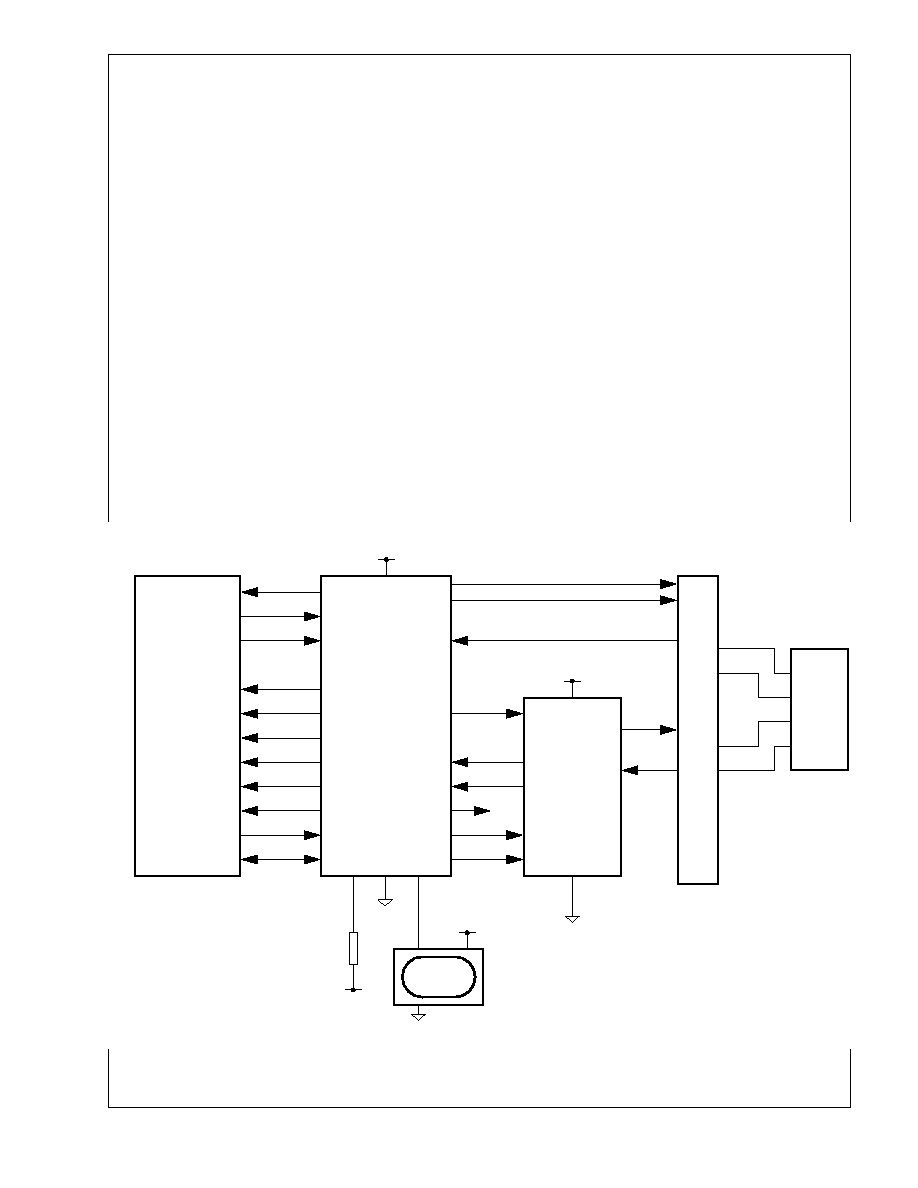
58
National Semiconductor
Version A
DP83840A 10/100Mb/s Ethernet Physical Layer
MEDIA
ACCESS
CONTROLLER
DP83840A
DP83223
TWISTER
MA
GNETICS
TX_CLK
TXD<3:0>
TX_EN
CRS
COL
RXD<3:0>
RX_CLK
RX_DV
RX_ER
MDC
MDIO
82
75, 76, 77, 78
74
66
65
55, 56, 57, 58
62
64
63
72
67
26, 25
24, 23
21, 20
17, 16
5, 6
8, 7
54
53
49
TD +/-
RD +/-
SD +/-
SPEED_10
ENCSEL
LBEN
15, 16
25, 24
20, 21
12
19
9, 8
2, 1
TXU+/-
TXS+/-
RXI+/-
V
CC
TXD +/-
RXD +/-
TD+
TD-
RD+
RD-
1
2
3
6
RJ-45
GND
50 MHz
0.005%
GND
GND
V
CC
OSCIN
V
CC
4.7k
33
4
2
X1
V
CC
5.0 DP83840A Application
5.1 Typical Board Level Application
Figure 20 shows a typical implementation of a 10/100
Mb/s Ethernet node application. This is given only to
indicate the major circuit elements of such a design. It is
not intended to be a full circuit diagram. For detailed
system level application information please contact your
National Semiconductor sales representative.
5.2 PLANE PARTITIONING
The recommendations for power plane partitioning
provided herein represent a more simplified approach
when compared to earlier recommendations. By
reducing the number of instances of plane partitioning
within a given system design, empirical data has shown
a resultant improvement (reduction) in radiated
emissions testing. Additionally, be eliminating power
plane partitioning within the system Vcc and system
ground domains, specific impedance controlled signal
routing can remain uninterrupted.
Figure 21 illustrates one possible example of plane
partitioning and allocation assuming a typical four-layer
board design. The minimum gap between any two
planes on a single layer must be held to 125 mils.
FIGURE 20. Typical 10/100 Ethernet Node Design Device Interconnection
By placing chassis ground on the top and bottom layers,
additional EMI shielding is created around the 125 Mb/s
signal traces that must be routed between the magnetics and
the RJ45-8 media connector. The example in Figure 17
assumes the use of Micro-Strip impedance control
techniques for trace routing.
5.3 POWER AND GROUND FILTERING
Sufficient filtering between the DP83840A power and ground
pins placed as near to these pins as possible is
recommended. Figure 22 suggests one option for device
noise filtering including special consideration for the sensitive
analog and PLL power pins. The actual connection from
ANAVCC to the 4
resistor should be implemented as a `fat
etch' (20 to 30 mils wide) of minimum length. The same
technique should be implemented for the connection from
PLLVCC to its 10
resistor.
The example provided in Figure 22 has been designed to
minimize the number of physical decoupling components
while still maintaining good overall device decoupling.
59
National Semiconductor
Version A
DP83840A 10/100Mb/s Ethernet Physical Layer
Layer 1 (top)
Layer 2
Layer 3
Layer 4 (bottom)
Chassis
Ground
System Ground
Ground
Plane:
VCC
Planes:
Chassis
Ground
Plane:
Plane:
DP83840A
DP83223
Magnetics
RJ45
System
System
DP83840A
DP83223
Magnetics
RJ45
System
VCC
DP83840A
DP83223
Magnetics
RJ45
DP83223
RJ45
Chassis Ground
Chassis Ground
DP83840A
Magnetics
Signal Routing
Signal Routing
Ground
Ground
System
VCC
Signal Routing
Signal Routing
System VCC
FIGURE 21. Power and Ground Plane Isolation
5.0 DP83840A Application (continued)
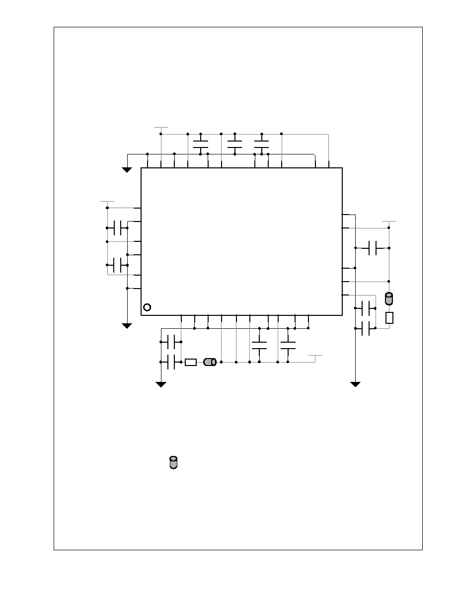
(Continued)
60
National Semiconductor
Version A
DP83840A 10/100 Mb/s Ethernet Physical Layer
FIGURE 22. DP83840A Power Supply Decoupling and Isolation
REFVCC
IO
VCC4
IO
VCC5
IO
VCC6
CGMVCC
CRMVCC
ECL
VCC
ANA
VCC
ANA
GND
PLLGND
RXGND
REFGND
TDGND
PCSGND
OGND
IOGND1
IOGND2
IOGND3
IOGND4
IOGND5
IOGND6
RCLKGND
CGMGND
CRMGND
FB
= FERRITE BEAD MURATA # BLM31A02PT
ALL CAPS ARE 16V CERAMIC
ALL RESISTORS ARE 1/8WATT, 5% TOLERANCE
RXVCC
TD
VCC
OVCC
PLLVCC
GND
PCSVCC
IOVCC1
IOVCC2
IO
VCC3
DP83840A
4
FB
VCC
GND
10
FB
GND
GND
VCC
VCC
0.01UF
10UF
0.01UF
0.01UF
0.01UF
0.01UF
0.01UF
10UF
10UF
10UF
0.01UF
VCC
5.0 DP83840A Application (continued)
0.01UF
OR TDK # TDK-ACB1608M-080

61
National Semiconductor
Version A
DP83840A 10/100 Mb/s Ethernet Physical Layer
6.0 Hardware User Information
6.1 Jabber/Timeout
Problem:
During the CRS_Jabber fix implemented on the
DP83840A, an unforeseen condition has resulted in
undesirable behavior in the CRS signal. There exists a
narrow region of improper CRS activity at the end of the
722
µ
s timeout where the device recognizes the Jabber
function.
Description:
If the data packet is essentially the same length as the
default 722
µ
s descrambler timeout CRS glitching will
occur. More specifically if the data packet terminates within
600ns of the 722
µ
s descrambler timeout, then the
descrambler won't have sufficient time to recognize the
necessary 15 idles before it times out. In that case the
parallel CRS_JAB (internal signal) will assert CRS to
indicate a jabber event.
Symptoms:
Since normal Ethernet packet activity is constrained to a
maximum packet size of 1514 bytes, which is about 121
µ
s,
the CRS glitch will not show up with standard packet
lengths. In the case that packets fall within the narrow
range for CRS glitching, that packet will be lost. The next
packet could be lost if the Inner-Packet-Gap (IPG) is too
small relative to the CRS glitch, which varies from
approximately 40ns to 600ns.
Solution/Workaround:
There is no current workaround to this problem. This
problem will be corrected in the next silicon revision.
6.2 Link Timer
Problem:
Link Timer State Machine Counter will not reset to 0 if the
Signal Detect falls while the Link Timer is in the
HYSTERESIS state.
Description:
If the link state machine is in the HYSTERESIS state
(Figure 24-15, clause 24.3.4.4 of 802.3u/D5.3), the timer
counts down from 500 to 0. AT 0, link timer is done, the
state machine transitions, and the timer is reset to 500. If
Signal Detect falls while the link state machine is in the
HYSTERSIS state, the state machine goes back to
LINK_DOWN, but the timer does not reset, since the reset
condition is based on the timer reaching 0. Thus when
Signal Detect becomes asserted, the counter will resume
counting where it left off, and not count the full 500
µ
s.
Symptoms:
If the network is operating normally and receiving good
data (Normal Link, substantial number of idles) no
problems will be observed. If Signal Detect is varying (bad
reception) the part would try to lock. If the lock was
successful the DP83840A would report Bad Start of
Stream Delimiter (Bad SSD) and the device would
disconnect. In a Repeater application the DP83840A would
see two Bad SSD's and disconnect that port. Only one
packet would be lost and then the part would reconnect. In
a node application the Media Access Controller (MAC)
would need to decipher if the data that was being received
was bad.
Solution/Workaround:
There is no current workaround to this problem. This
problem will be corrected in future products.
6.3 Link LED, Link Status Bit
Problem:
The Link LED which indicates good link status derives its
signal from energy present on Signal Detect (SD+/-). The
Link Status bit (bit 2) in the Basic Mode Control Register
(00h) represents true link and derives its status from
different conditions than the Link LED.
Description:
The Basic Status Register Link status operation is as
follows:
This bit represents true link. In 100Base-TX it is Cipher in
Sync. Cipher-in-sync is based on receiving 15 idle symbols
after Link Test Fail (LTF) is low.
If link status is down it is updated in the bit, next clock
cycle.
To get the link status, the user has to read the register
twice. The last read will give the correct status, after the
first read bit is updated with the new link status. This
register bit operation is based on IEEE 802.3u (page 31,
802.3u/D5.3).
Symptoms:
It is possible for Link LED to have a different value than the
Link Status Register bit.
Solution/Workaround:
For True Link, read the register status bit twice. The
operation of the Link is IEEE 802.3 compliant.
6.4 PHYAD[3] and SPEED_100
Problem:
When using the SPEED_100 output (pin 89) of the
DP83840A to control external circuitry such as certain
switch elements for Common Magnetics implementations,
care must be taken in order to avoid electrical contention
between the effective load of the external circuitry and the
power-on/reset latch-in value of the PHYAD[3] input (also
pin 89).
Description:
The standard procedure for latching in the desired PHY
Address of the DP83840A during power-on/reset is to
resistively tie each of the five PHYAD pins either high or
low such that one of the 32 possible addresses is
programmed into the device. If the dual purpose PHYAD
pin is connected to an external load which contends with
the intended pull-up or pull-down resistor, the wrong logic
level may be latched into the device which will result in an
invalid (unintended) PHY address. This, in turn, will impair
serial MII management of the PDP83840A.
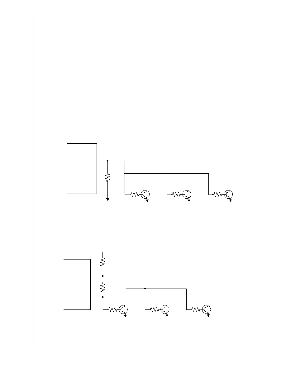
6.0 Hardware User Information
(Continued)
62
National Semiconductor
Version A
DP83840A 10/100 Mb/s Ethernet Physical Layer
Symptoms:
An improper five bit PHY Address is latched into the
DP83840A upon power-on/reset.
Solution/Workaround:
In order to guarantee that a logic low level is latched-in to
PHYAD[3] upon power-up/reset, it is recommended that a
4.7k
resistor be connected from this pin directly to
ground. Figure 23 illustrates the recommended connection
of external circuitry when using PHYAD[3] / SPEED_100 to
control transistors used for Common Magnetics
implementations.
In order to guarantee that a logic high level is latched-in to
PHYAD[3] upon power-up/reset, it is recommended that a
1.0k
resistor be connected from this pin directly to Vcc
and that a 1.2k
resistor be connected in series between
this pin and the transistor control circuitry. It is important to
take note that the base resistor values (each 100
in this
case) are lowered in order to compensate for the series
1.2k
resistor with respect to proper transistor biasing.
Figure 24 illustrates the recommended connection of
external circuitry when using PHYAD[3] / SPEED_100 to
control transistors used for Common Magnetics
implementations.
6.5 Collision De-Assertion Time
Problem:
In 100 Mb/s operation, the Collision De-Assertion time
violates the IEEE802.3u specification.
Description:
The Collision De-Assertion time which is determined from
when TX_EN is deasserted to COL going low is specified
at 40ns maximum per IEEE 802.3u/D5.3 section
22.2.4.1.9. This is a test mode function. The DP83840A
has a specification of 87ns maximum.
TXREF
TXO+ Term
TXO- Term
PHYAD[3]/
SPEED_100
DP83840A
4.7k
1.2 k
1.2 k
1.2 k
Q3
Q2
Q1
GND
All resistors are 1/8th Watt, +/- 5% tolerance
Figure 23. Recommended Control Circuitry and Valid PHYAD[3] Logic Low Latch-in Value
Vcc
TXREF
TXO+ Term
TXO- Term
PHYAD[3]/
SPEED_100
DP83840A
1.0 k
All resistors are 1/8th Watt, +/- 5% tolerance
Q3
Q2
Q1
1.2k
100
100
100
Figure 24. Recommended Control Circuitry and Valid PHYAD[3] Logic High Latch-in Val
ue
6.0 Hardware User Information
(Continued)
63
National Semiconductor
Version A
DP83840A 10/100 Mb/s Ethernet Physical Layer
Symptoms:
The COL signal could go low up to 87ns after TX_EN goes
low.
Solution/Workaround:
There is no current workaround to this test mode function.
In a network environment, this will not be a problem.
6.6 Synchronization of Idle
Problem:
In 100 Mb/s operation, descrambler violates the TP-PMD
specification of 12 idle times or 60 cipher bits.
Description:
The DP83840A will acquire descrambler synchronization in
13 symbols. However, due to latency and pipeline delays,
the DP83840A can not provide valid decoded data less
than 16 Idle symbols.
Symptoms:
If the Idle stream is between 13 and 16 symbols, the
descrambler will synchronize to the transmit data, yet the
Start of Frame Delimiter (SFD) will be lost resulting in the
detection of a Bad_SSD. The subsequent packet following
the next idle stream will be lost.
Solution/Workaround:
The minimum number of consecutive idles required for a
proper network operation is sixteen. There is no current
workaround to this problem. Since the minimum IPG in a
network system is greater than 16 symbols, there is no real
system impact for this problem.
6.7 10 Mb/s Differential Output Voltage
Problem:
Based on the characterization data across fab process,
voltage, and temperature, the DP83840A is on the high
side of the Vod specification.
Description:
The Vod measured without resistors connected to the RTX
and REQ pins, ranges from 2.4V to 3.1V. IEEE 802.3
specifies the differential output voltage to be between 2.2V
to 2.8V (zero to peak).
Symptoms:
National Semiconductor believes that there will be no
system ramifications with higher than specified Vod
voltages. The worse case scenario would be a slight
increase in cross-talk in between the twisted pair cables.
Solution/Workaround:
If desired, the Vod voltage can be modified by connecting
resistors from RTX (pin 28) and REQ (pin 29) to ground.
Figure 25 illustrates the recommended connection of
external circuitry which determines the Vod amplitude and
shape. This will cause the Vod voltage to be lowered.
Based on the data taken from the laboratory, National
Semiconductor recommends starting with a 100k
resistors for both the RTX and REQ pins. The Vod will be in
the range in between 2.2V to 2.9V when the 100k
resistors are used. The value of resistor you choose may
be different based on your board layout and selection of
components such as pulse transformers.
6.8 10Base-T Transmit Differential Output
Impedance
Problem:
Based on the characterization data across fabrication
process, voltage, and temperature, the DP83840A does
not meet the letter of tIEEE 802.3 10BaseT specification on
the 10 Mb/s Transmit Differential Output Impedance (which
is measured as return loss).
Description:
The IEEE 802.3 10BaseT standard requires a return loss
of 15dB or better at all times (during transmit state or idle
state) over the frequency range of 5 MHz to 10 MHz with a
cable impedance range from 85
to 111
. The DP83840A
characterization data shows that while the device meets
the 15dB return loss specification during transmit and
during idle on average, some devices may have return loss
of less than 15dB during idle.
DP83840A
Pin 28 (RTX)
Pin 29 (REQ)
100 k
100 k
Figure 25. Recommended External Circuitry to Control the Amplitude and Shape of Vod
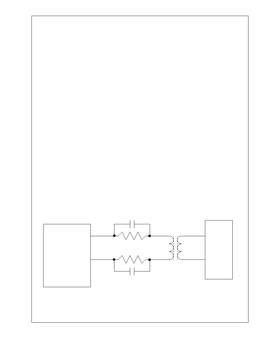
6.0 Hardware User Information
(Continued)
64
National Semiconductor
Version A
DP83840A 10/100 Mb/s Ethernet Physical Layer
Symptoms:
National believes that there will be no system ramification
due to the DP83840A not meeting the IEEE specification
for return loss. National Semiconductor has done extensive
system testing with DP83840A's that have return loss in
the range of 4-6dB, and did not see any degradation in
system performance.
Solution/Workaround:
To improve the return loss at idle, National Semiconductor
recommends that 1000pF capacitors be place in parallel to
the 10.5
termination resistors connected to the TXU+/-
pins. Figure 26 illustrates the recommended connection of
external components to improve return loss.
6.9 Low Power Mode
Problem:
The DP83840A sometimes fails to Auto-Negotiate when
switching from 100 Mb/s link partner to a 10 Mb/s link
partner when the low power pin (pin 2) is driven by
Speed_100/PhyAdr<3> (pin 89).
The low power mode works when used in a 100 Mb/s only
operation.
Description:
Any application using the DP83840A (with the low power
pin driven by the Speed_100 pin) will sometimes fail to
Auto-Negotiate to the 10 Mb/s link partner that has first
established a link with a 100 Mb/s link partner and then is
disconnected from the 100 Mb/s link partner and then
connected to a 10 Mb/s link partner. The reason for this is
that in 100 Mb/s mode, the part will be configured for low
power mode and shut down the 10 Mb/s and Auto-
Negotiation circuitry in the DP83840A and when it tries to
connect to a 10 Mb/s link partner the 10 Mb/s and Auto-
Negotiation circuitry might not be fully powered up.
Symptoms:
When this problem occurs, no link will be established with
the 10 Mb/s link partner and the FLP signal being sent by
the DP83840A will be half it's normal amplitude. This
indicates that the 10 Mb/s section of the chip has not
powered up properly.
Solution/Workaround:
It is recommended that in 10/100 application that the low
power mode of the device not be used.
In 100 Mb/s only applications, it is recommended that the
low power pin be pulled high through a 4.7k
resister.
6.10 Software Reset
Problem:
Hardware Configuration pins require a (4.7k
or less) pull
up/down resistor to insure that the Physical Address is
stable at latching time.
Description:
The following is an explanation of events based on
software reset:
1. First high byte is written via MDIO
2. Software reset is true for the next 500ns.
3. At synchronous de-assertion of the reset all mode pins
and Phy Address pins are latched.
4. Output enables for Phy Address pins are disabled (they
will become inputs) from start of the reset to 1700ns after
reset assertion.
5. Within 250ns from assertion of software reset, the phy
address has to be stable. This implies that the RC time
constant should be faster than 250ns so that Phy address
will be latched correctly with reset synchronous de-
assertion.
6. DP83840A Phy Address pin drivers have been modified
to provide more drive current than the DP83840. This will
increase the capacitance at the pin, hence the resistance
will need to be reduced accordingly to keep the time
constant low.
DP83840A
Pin 25 (TXU-)
Pin 24 (TXU+)
RJ45
1:2
10.5
10.5
1000pF
1000pF
2
1
Figure 26. Recommended External Circuitry to Improve Transmit Return Loss

6.0 Hardware User Information
(Continued)
65
National Semiconductor
Version A
DP83840A 10/100 Mb/s Ethernet Physical Layer
7. Reduce the pull up/down resistance to 4.7k
to make
the Phy Address stable at the latching time of 250ns. If the
capacitance at the node is large due to a particular
application, then the resistance will need to be lowered
even further.
Symptoms:
If the time constant at the Phy Address pins is in excess of
250ns then the proper hardware configurations values may
not be latched into the device after the software reset is
initiated.
Solution/Workaround:
Use 4.7k
resistors or resistors with lower values on all
PhyAddr pull up/down pins.
6.11 Receive Error Counter
Problem:
When receiving two back to back packets that have receive
errors (symbol errors), the DP83840A under certain
conditions records only the second symbol error (i.e. the
Receive Error Counter only gets incremented once for both
errors).
Description:
When a symbol error occurs at the very end of a packet, it
doesn't get reflected in the Receive Error Counter (Bits
15:0, Address 15h) until the next packet is in progress (an
internal synchronization issue between the receive clock
domain and the register clock domain). Normally, this isn't
a problem, the counter gets updated during the next
packet. The problem occurs when the packet with the "late"
symbol error backs up against another packet with a
symbol error. In that case, the counter only gets
incremented once for both errors.The end result is that the
counter misses a count.
Symptoms:
The Receive Error Counter, bits 15:0 in the Receive Error
Counter Register (15h), under certain conditions can
record a value in the register that is less than the true
receive error count.
Solution/Workaround:
There are no workarounds for this problem. This problem
will be fixed in future products.
6.12 Auto-Negotiation Test Compliancy
Problem:
During Auto-Negotiation conformance testing, by an
independent lab, four test conformance issues were
uncovered.
We do not believe these four test
conformance issues will cause any system issues. The
four issues are:
1.) The part improperly enters the Acknowledge Detect
state upon receiving two groups of four inconsistent FLPs,
i.e.(the data in the FLPs alternate)
2.) The value of the nlp_test_min_timer is between 3.8ms
and 4.9ms, which is below the 5ms minimum requirement.
3.) The value of the data_detect_min_timer is valid except
when a pulse is received before the timer has expired.
4) The value of link_fail_inhibit_timer is 640ms, which is
below the 750ms minimum requirement.
Description:
Described below are the four conformance tests that the
DP83840A failed. Currently IEEE does not have standard
tests to test for conformance. The tests performed by the
outside lab correspond to the four issues listed above.
Test 1: The DP83840A is sent two groups of four FLP
bursts with a inter-group gap greater than
nlp_test_max_timer of 150ms. An example of the FLP
burst is shown below:
ABAB (Inter-group gap) ABAB
Where A represents a Link Code Word advertising a
technology such as 10 Mb/s half-duplex and B represents
a Link Code Word that is advertising a different technology
such as 100 Mb/s full-duplex.
When this ABAB (Inter-group gap) ABAB pattern is
received by the DP83840A, it will set the ACK bit.
Test 2: The DP83840A when sent four FLPs with a burst to
burst gap less than the 5ms speck. will set the ACK bit.
Test 3: The DP83840A when sent four FLPs with a
`erroneous' extra pulse after one of the clock pulses does
not ignore the extra pulse and as a result, the ACK bit is
not set.
Test 4: The DP83840A is sent a sequence of FLPs to
cause it to enter the FLP Link Good Check state. Upon
entering this state, the DP83840A should cease FLP
transmission and see all link_status indications as FAIL.
After link_timer and break_link_timer expires, the
DP83840A should resume FLP transmission. The
DP83840A failed the Link_fail_inhibit_timer test with a
value of 640ms which is below the 750ms limit.
Symptoms:
It is our opinion that the four issues found by the outside
lab will not affect system performance. Listed below are the
reasons we believe there will not be any system issues.
Issue 1: In a real network, the Auto-Negotiation protocol is
such that, once enabled, the FLP bursts should be sent
constantly, not in groups of 2, 4, 8, etc., with a number of
seconds in between FLP bursts (No inter-group gap). The
outside lab pointed out that the DP83840A implementation
works fine when the FLP bursts are constant, even if the
data within the bursts change.
Issue 2: The function of the NLP test timer is to ensure that
the FLP bursts are not spaced too close together and to
ensure that the data pulse to clock pulse timing is not too
long. The transmit specification for FLP burst spacing is
8ms min. Most, if not all applications center the FLP burst
spacing around 16ms. The data pulse to clock pulse timing
should be approximately 78
µ
s maximum. As long as the
transmitter that is sending FLPs to the DP83840A is within
specifications, then having the NLP timer expire 1.2ms
early will not have any affect on Auto-Negotiation.
Issue 3: The extra `erroneous' pulse is used to simulate
noise injected into the FLP stream which can potentially
corrupt the FLP burst. The Auto-Negotiation transmit
protocol requires the transmitter to send the same FLP
burst repeatedly (not just four times). Thus, if the
DP83840A receives an extra `erroneous' pulse, then it will
take a few additional FLP bursts to set the ACK bit.
Issue 4: The link_fail_inhibit_timer is used to give the link a
chance to become good once a technology is selected.
The DP83840A will establish good link within

6.0 Hardware User Information
(Continued)
66
National Semiconductor
Version A
DP83840A 10/100 Mb/s Ethernet Physical Layer
approximately 250ms max., as long as it is getting valid
signals. Since the link_fail_inhibit_timer only needs to be
larger than the worst case link up time for all technologies
supported (10BASE-T and 100BASE-TX link up times are
much smaller than 640ms), then 640ms vs.750ms will not
cause any system problems.
Solution/Workaround:
There are no plans on fixing any of the issues on the
DP83840A. We will incorporate changes to fix the above
issues in future products to insure our products a
specification compliant.

67
National Semiconductor
Version A
DP83840A 10/100 Mb/s Ethernet Physical Layer
7.0 Software User Information
7.1 100 Mb/s Full Duplex Log-On
Problem:
Certain Software drivers that were developed for the
DP83840 do not account for the longer auto-negotiation
time that is required for the DP83840A to complete Auto-
Negotiation. This is discussed in the IEEE specification
802.3U from draft D2 to D5. The Auto-Negotiate time has
increased from 1 second to approximately 3 seconds
between the two devices.
Description:
The problem can be seen when the server or the client
physical layer device is the DP83840A. When the client is
attempting to log on to the server the user will see CRC
errors occurring until the client times out and disconnects.
The driver software that was written for the DP83840
needs to be modified to account for the additional time per
the specification 802.3(D5.3) that is required for the
DP83840A to complete Auto-Negotiation.
Symptoms:
A Novell server and a Novell DOS client that are connected
via a crossover cable will not log on to 100 Mb/s Full
Duplex with the DP83840A in the client or the server.
Solution/Workaround:
The solution is to modify the driver software to
accommodate the longer Auto-Negotiation time that is
required. The basic script should be the following:
A.) Wait for auto-negotiation to complete (Three seconds)
B.) Verify whether the auto-negotiation is completed by
reading BSMR bit<5>.
C.) If BMSR<5> is set read the BMSR to update the link
status BMSR<2>.
D.) If the BMSR<2> is set, read the PAR (19h) register.
PAR bits<7:6> reflect the Duplex_STAT and Speed_10
status.
7.2 Auto-Negotiation to Link Sending 100 Mb/s
Scrambled Idles.
Problem:
The DP83840A when Auto-Negotiating with a 100 Mb/s
link partner that is sending out 100 Mb/s scrambled idles
can, for specific cable lengths, approximately 35 to 41
meters or equivalent attenuation, misinterpret the 100 Mb/s
scrambled idles as FLP's (Fast Link Pulses), thereby
causing a false MLF (Multiple Link Fault) condition which
hangs the Auto-Negotiation process (No link established).
This problem only occurs with the above scenario and
does not affect other methods of linking such as Auto-
Negotiating to a 10 Mb/s link partner, Auto-Negotiating to a
Auto-Negotiation link partner, forcing the DP83840A into
100 Mb/s mode and linking to a 100 Mb/s link partner, and
forcing the DP83840A into 10 Mb/s mode and linking to a
10 Mb/s link partner.
Description:
When Scrambled 100 Mb/s idles are transmitted, the
energy is dispersed across the spectrum from 1MHz to
31.25 MHz. Some of this energy is aliased in the 10 Mb/s
domain and for specific cable lengths, between 35meters
to 41meters or equivalent attenuation, is falsely detected
as FLP pulses. At these specific cable lengths, the Auto-
Negotiation receive state machine will misconstrue enough
FLP pulses such that it fits the FLP template, thereby
notifying the arbitration state machine of the receipt of FLP
pulses.
At the same time the misconstrued FLP's are being
detected, the arbitration state machine is moving through
the parallel detection path. This causes the arbitration state
machine to think that it is receiving both FLP pulses and
100 Mb/s scrambled idles, thereby, causing a parallel
detection fault (MLF bit 4 set high in the Auto-Negotiation
expansion register (06h)), and hanging the Auto-
Negotiation process.
Symptoms:
This problem only occurs when a system using the
DP83840A is in Auto-Negotiation mode and tries to
establish link with a system that is sending out 100 Mb/s
scrambled idles and the cable length is approximately
35meters to 41 meters or equivalent attenuation. When the
problem occurs the following will be observed:
A.) Pin 38 (Link LED) will go low indicating 100 Mb/s
activity.
B.) The Multiple Link Fault bit (bit 4) of the Auto-
Negotiation Expansion Register (06h) is HIGH, indicating
the DP83840A thinks FLP's were being received.
C.) The Link Status bit (bit 2) of the Basic Mode Status
Register (01h) is LOW, indicating link not established.
D.) The Auto-Negotiation Complete bit (bit 3) in the Basic
Mode Status Register (01h) is LOW, indicating Auto-
Negotiation not complete.
Solution/Workaround:
For existing products using the DP83840A the following
can be done to work around the problem:
A.) Manually configure the system using the DP83840A
into 100 Mb/s mode through software. Many installation
programs already support this capability.
B.) Modify software driver to detect fault condition. A
proposed software driver work around for this problem
follows:
The workaround is based upon the concept that a
DP83840A that is failing to complete negotiation is
attempting to negotiate with a non-Auto-Negotiation-
capable 100 Mb/s link partner. In that case, the software
driver can force the local node/port directly into 100 Mb/s
Half-Duplex mode to complete negotiation. Half-Duplex
100 Mb/s mode is what the Auto-Negotiation logic would
select had the fault not occurred. The total time that Auto-
Negotiation will take to complete is under 3 seconds.
Therefore, the proposed software driver should implement
the following:
Reset the 840A the DP83840A by writing 8000h to BMCR
register, or re-start Auto-Negotiation by writing 1200h to
BMCR register. Wait 3 seconds then read bit 5 (Auto-
Negotiation Complete bit) and bit 2 (Link_Status bit) in the

7.0 Hardware User Information
(Continued)
68
National Semiconductor
Version A
DP83840A 10/100 Mb/s Ethernet Physical Layer
Basic Mode Status Register (01h). The Link Status bit must
be read twice, since it's a latched bit. If bit 2 and bit 5 are
set to a logic 1, then Auto-Negotiation completed
successfully. Bits 6 and 7 in the Phy Address Register
(19h) contain the information on Speed and Duplex (FD/
HD).
If the Link_Status bit OR the Auto-Negotiation Complete bit
are still logic 0 (bits 2 and 5) in the Basic Mode Status
Register (01h), then negotiation did not complete. Read bit
4 (Multiple Link Fault) in the Auto-Negotiation Expansion
Register (06h). ANER bit 4 must be read twice, since it's a
latched bit. If the Multiple Link Fault bit is set to a logic 1,
then the device can be forced into 100 Mb/s Half-Duplex
operation via register control.
On the Basic Mode Control Register (00h) set bit 12 (Auto-
Negotiation Enable) to a logic 0, set bit 13 (Speed
Selection) to a logic 1 for 100 Mb/s operation, and bit 8 to
logic 0 for Half-Duplex operation. (i.e. write 2000h to the
Basic Mode Control Register). This disables Auto-
Negotiation and puts the part into 100 Mb/s mode.
Check Link Status (bit 2 of Basic Mode Status Register) bit
by reading BMSR register twice. If bit 2 is set to "1", then
the local node/port is linked to the non Auto-Negotiation
100 Mb/s partner.
If bit 2 of the BMSR is not set, then force the device into 10
Mb/s mode by writing 0000h to BMCR register (00h).
Check Link Status (bit 2 of Basic Mode Status Register) bit
by reading BMSR register twice. If bit 2 is set to "1", then
the local node/port is linked to the non Auto-Negotiation 10
Mb/s partner.
National is evaluating a silicon fix to correct this problem.
Please contact your Sales Representative for the current
status.
7.3 840A Auto-Negotiating to Legacy Devices
Problem:
The DP83840A will not always complete Auto-Negotiation
when Auto-Negotiating with a 100 Mb/s or 10 Mb/s link
partner that is sending out packet data before link has been
establish.
Description:
The DP83840A in Auto-Negotiation mode is not always
able to establish link with a 100 Mb/s link partner that is
sending out scrambled packet data. The reason for this is
that the DP83840A is expecting to see only 100 Mb/s idles,
Fast Link Pulses (FLPs), or Normal Link Pulses (NLPs) and
not scrambled packet data. When the DP83840A sees
scrambled packet data, it can be misconstrued as NLPs
and FLPs, which confuses the Auto-Negotiation state
machine.
The DP83840A in Auto-negotiation mode may not able to
complete Auto-Negotiation with a 10 Mb/s link partner that
is sending out packets prior to getting a good link. The
reason for this is that the DP83840A can mis-identify some
specific 10 Mb/s packet energy as 100 Mb/s data. When
the DP83840A receives those specific 10 Mb/s packet, it
will get confused on which speed to detect.
The 802.3U IEEE specification does not allow transmission
of data prior to getting Good Link Status. The DP83840A is
compliant to this specification, but some Legacy devices
are not, such as the DP83840, which will transmit data
before Good Link Status is achieved. The problem with the
10 Mb/s is very limited. It only happen when Auto-
Negotiation is initiated by software (i.e. writing 1200h to
BMCR), and does not happen with un-plugging and re-
plugging of cable, or H/W or S/W reset. Since there are
very few 10 Mb/s only DP83840 Legacy devices out in the
market, the possibilities of not able to Auto-Negotiate with
10 Mb/s device is very minimal.
Symptoms:
When the DP83840A receives packet data during Auto-
Negotiation, the Auto-Negotiation state machine thinks that
there are multiple links present and sets the Multiple Link
Fault Bit (bit 4) in the AUTO-NEGOTIATION EXPANSION
REGISTER (06h). The problem can be seen with 64 byte
100 Mb/s packets with Inter-Packet-Gaps (IPG) of less
than 5us, or 64-128 byte 10 Mb/s packets with IPG of
9.6us.
Solution/Workaround:
The same workaround described in 011.E (Auto-
Negotiating to Link Partner Sending 100 Mb/s Scrambled
Idles) will also work with this problem:
A.) Manually configure the system using the DP83840A
into 100 Mb/s or 10 Mb/s mode through software. Many
installation programs already support this capability.
B.) Modify software driver to detect fault condition.
7.4 HBE Disable in 10 Mb/s Repeater Mode
Problem:
According to the 802.3 IEEE specification Heart Beat
Enable (HBE) must be disabled when used in
repeaters.The DP83840A when put into 10 Mb/s repeater
mode does not disable HBE automatically and must be set
manually.
Description:
Approximately 1.6
µ
s after the end of a packet the COL line
will become active for approximately 1.3
µ
s. A repeater
using the COL line to determine collisions or gather
collision statistics will misinterpret the HBE signal as a valid
collision.
Symptoms:
With HBE enabled in repeater mode the COL line will
become active after the end of packet and cause the
repeater to falsely detect collision activity.
Solution/Workaround:
HBE can be disabled by writing a 0 to bit 4 (HBE) in the
10BASE-T CONFIGURATION REGISTER (1Ch).
HBE can also be disabled by putting the part is in Full-
Duplex mode.
7.5 CRS Glitching in10 Mb/s Repeater Mode
Problem:
When the DP83840A is put into 10 Mb/s repeater mode
and receives a non-101010... jam pattern, Carrier Sense
(CRS) will glitch during collision. This will cause problems
when used in repeater applications where CRS is used to
determine collisions. The collision signals from the
DP83840A behave normally.
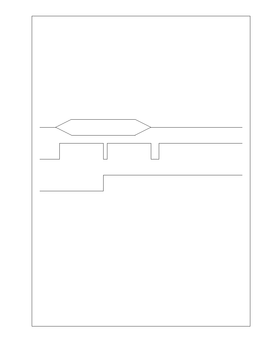
7.0 Hardware User Information
(Continued)
69
National Semiconductor
Version A
DP83840A 10/100 Mb/s Ethernet Physical Layer
Description:
The DP83840A when in 10 Mb/s Repeater Mode does not
conform to 802.3 IEEE specification for Carrier Sense
(CRS). The specification states that CRS becomes active
whenever the receive input becomes active and in-active
when there is no activity. The DP83840A uses its' internal
Phase Lock Loop (PLL) to gate CRS. This causes CRS to
glitch when the PLL switches from Receive mode to
Transmit mode and when the PLL switches from Transmit
to Receive mode. The switching of modes is what occurs
during collisions.
Symptoms:
When the part is receiving a packet and then TX_EN is
asserted, CRS will glitch twice, once following the rising
edge of TX_EN and once following the end of RXI+/-. This
is illustrated in Figure 27.
When the part receives a JAM signal that has a
combination of 5 MHz and 10 MHz signals, CRS will glitch.
CRS behaves normally when a 101010... JAM pattern is
received. All repeaters and most MACs send out 101010...
JAM signals, but there are a few MACs that will send out
pseudo-random 5/10 MHz data.
Solution/Workaround:
Putting the part into Full-Duplex mode eliminates the CRS
glitching problem. However, when the part is in Full-Duplex
mode the COL pin (pin 65) will not indicate if collisions
have occurred.
RXI +/-
CRS
TX_EN
FIGURE 27. CRS Glitching

70
Version A
DP83840A 10/100 Mb/s Ethernet Physical Layer
8.0 Electrical Specifications
8.1 RATINGS AND OPERATING CONDITIONS
8.1.1 Absolute Maximum Ratings
Supply Voltage (V
CC
)
-0.5 V to 7.0 V
Input Voltage (DC
IN
)
-0.5 V to V
CC
+ 0.5 V
Output Voltage (DC
OUT
)
-0.5 V to V
CC
+ 0.5 V
Storage Temperature
-65
o
C to 150
o
C
ECL Signal Output Current
-50mA
ESD Protection
2000 V
8.0 Electrical Specifications
8.1.2 Recommended Operating Conditions
Min Typ Max Units
Supply voltage (V
dd
)
4.75
5.0
5.25
V
Ambient Temperature (T
A
)
0
70
o
C
REFIN Input Frequency (25
MHz)
-50
+50
ppm
REFIN Input Duty Cycle
35
65
%
OSCIN Input Frequency (50
MHz)
-50
+50
ppm
OSCIN Input Duty Cycle
35
65
%
Crystal Specifications:
Crystal Center Frequency
(X
FC
)
20
MHz
Crystal Freq. Stability (X
STAB
)
(Over Temperature)
-50
+50
ppm
MAXIMUM JUNCTION
130 degrees Celsius
MAXIMUM CASE
110 degrees Celsius
8.2 DC Specifications
Symbol
Pin Types
Parameter
Conditions
Min
Typ
Max
Units
V
IH
I
I/O
I/O, Z
(excluding RXI+/-
and RD+/-)
Input High
Voltage
2.0
V
AN0 and AN1
Input Pins
I
IH
= 2 mA
V
CC
-
1.0
V
V
IL
I
I/O
I/O, Z
(excluding RXI+/-
and RD+/-)
Input Low
Voltage
0.8
V
AN0 and AN1
Input Pins
I
IL
= -2 mA
1.0
V
V
IM
AN0 and AN1
Inputs Only
Input Mid Level
Voltage
Pin Unconnected
(V
CC
/2)
-0.25
(V
CC
/2)
(V
CC
/2)
+0.25
V
I
IH
I
I/O
I/O, Z
(excluding RXI+/-
and RD+/-)
Input High
Current
V
IN
= V
CC
10
µ
A
X1 Input
X2 = N.C.
-100
µ
A
8.1.3 Thermal Characteristics
No Airflow
0.5W / 1.0W / 2.0W
225 LFPM
1.0W
500 LFPM
1.0W
900 LFPM
1.0W
Theta Junction to Case
(T
jc
) @ 1.0W
Theta Junction to Ambient
(T
ja
) degrees Celsius/Watt
36.3 / 35.9 / 34.3
28.7
24.3
21.9
10.5

8.0 Electrical Specifications
(Continued)
71
Version A
DP83840A 10/100 Mb/s Ethernet Physical Layer
I
IL
I
I/O
I/O, Z
(excluding RXI+/-
and RD+/-)
Input Low
Current
V
IN
= GND
10
µ
A
X1 Input
X2 = N.C.
100
µ
A
TMS, TDI, TRST
Inputs
1
mA
V
OL
O, Z
I/O
I/O, Z
Output Low
Voltage
I
OL
= 4 mA
0.4
V
V
OH
O, Z
I/O
I/O, Z
Output High
Voltage
I
OL
= -4 mA
V
CC
-
0.5
V
TX_CLK Pin
V
CC
-
1.5
V
I
OZ1
I/O, Z
O, Z
TRI-STATE
Leakage
V
OUT
= V
CC
10
µ
A
I
OZ2
I/O, Z
O, Z
TRI-STATE
Leakage
V
OUT
= GND
-10
µ
A
R
OL
TXU+/-
TXS+/-
Low Level
Output
Impedance
5
R
OH
TXU+/-
TXS+/-
High Level
Output
Impedance
5
V
OD
TXU+/-
TXS+/-
Differential
Output Voltage
Open Circuit
+/-2.5
V
C
IN1
I
CMOS Input
Capacitance
8
pF
C
IN2
I
ECL Input
Capacitance
5
pF
C
OUT1
O
Z
CMOS Output
Capacitance
10
pF
C
OUT2
O
Z
ECL Output
Capacitance
5
pF
V
TH1
RXI+/-
10BASE-T
Receive
Threshold
300
585
mV
V
TH2
RXI+/-
10BASE-T
Receive Low
Squelch
Threshold
175
300
mV
V
DIFF
I (ECL)
Input Voltage
Differential
Both inputs tested
together
150
mV
V
CM
I (ECL)
Common Mode
Voltage
Both Inputs Tested
Together, V
DIFF
= 300
mV
V
CC
-
2.0
V
CC
-
0.5
mV
8.2 DC Specifications
Symbol
Pin Types
Parameter
Conditions
Min
Typ
Max
Units

72
Version A
DP83840A 10/100 Mb/s Ethernet Physical Layer
8.0 Electrical Specifications
I
INECL
I (ECL)
Input Current
V
IN
= V
CC
or GND
-200
200
µ
A
V
OHECL
O (ECL)
Output High
Voltage
V
IN
= V
IHmax
V
CC
-
1.075
V
CC
-
0.830
V
V
OLECL
O (ECL)
Output Low
Voltage
V
IN
= V
ILmax
V
CC
-
1.860
V
CC
-
1.570
V
I
CC
power
Total Supply
Current
10/100 Mb/s Operation
(LOWPWR = 0)
315
335
mA
power
Total Supply
Current
100 Mb/s Operation
(LOWPWR = 1)
270
290
mA
8.2 DC Specifications
Symbol
Pin Types
Parameter
Conditions
Min
Typ
Max
Units
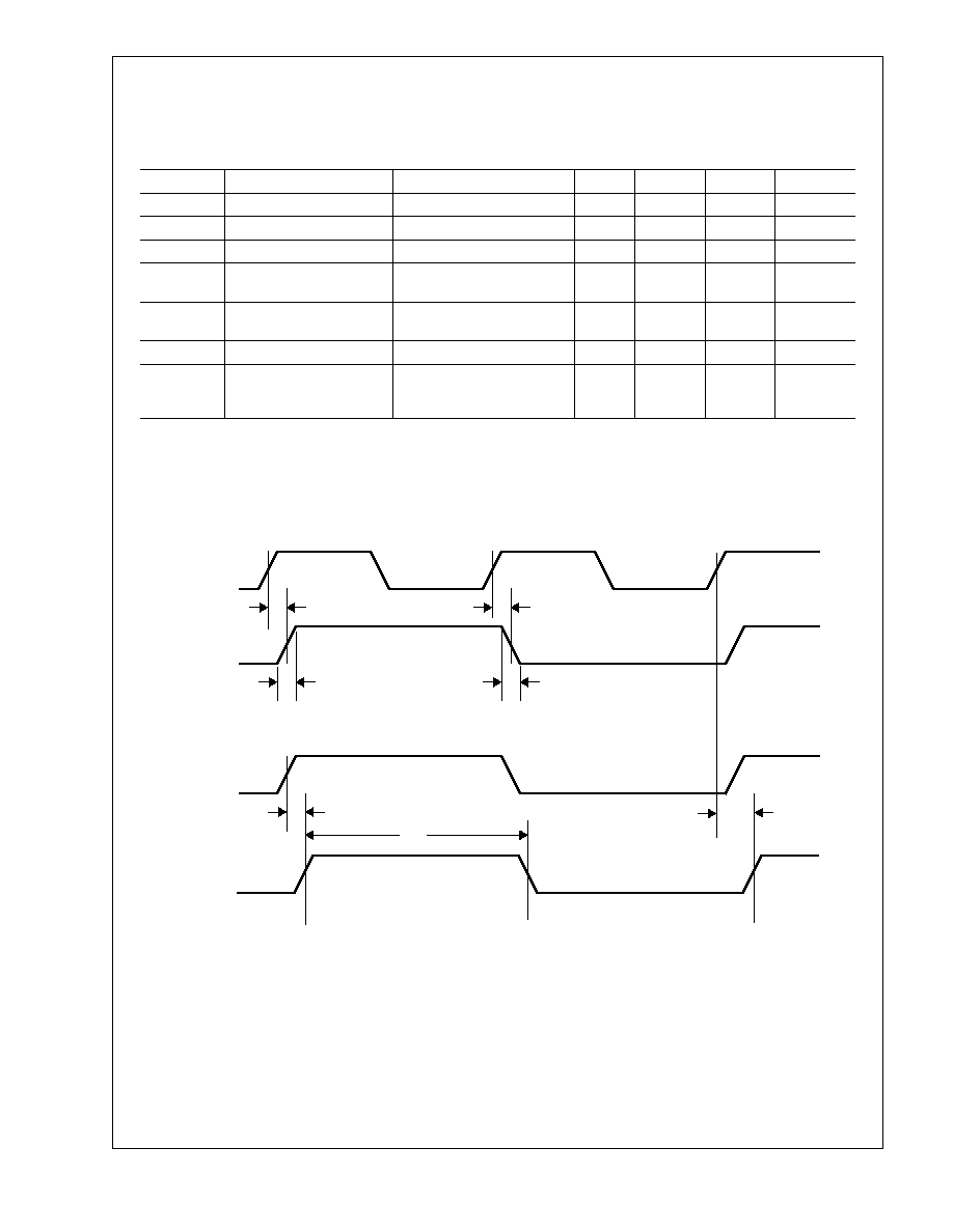
73
Version A
DP83840A 10/100 Mb/s Ethernet Physical Layer
8.0 Electrical Specifications
8.3 CLOCK TIMING
8.3.1 Clock Reference and Clock Generation Timing
Parameter
Description
Notes
Min
Typ
Max
Units
T1
OSCIN to CLK25M Delay OSCIN = 50 MHz
0
30
40
ns
T2
CLK25M Rise Time
10% to 90%
5
ns
T3
CLK25M Fall Time
90% to 10%
5
ns
T4
OSCIN to TX_CLK Delay 10 Mb/s Operation (MII
Nibble Mode)
10
ns
T4a
OSCIN to TX_CLK Delay 10 Mb/s Operation (MII
Serial Mode)
10
ns
T5
REFIN to TX_CLK Delay
100 Mb/s Operation
-3.0
+3.0
ns
T6
TX_CLK Duty Cycle
10 Mb/s Nibble (2.5 MHz),
10 Mb/s Serial (10 MHz)
100 Mb/s Nibble (25 MHz)
35
65
%
OSCIN
CLK25M
REFIN
TX_CLK
T1
T5
T1
T4
T2
T3
T6
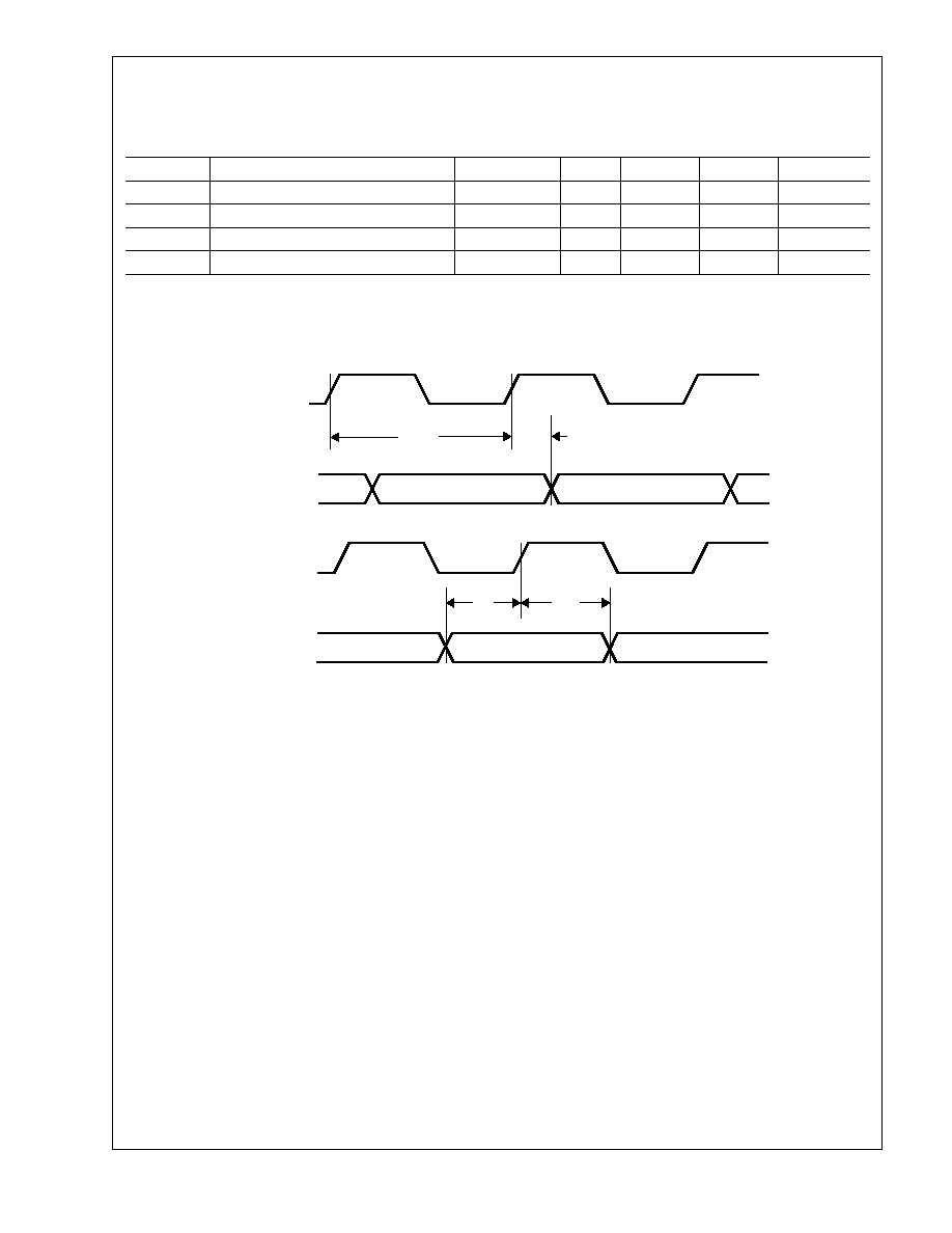
8.0 Electrical Specifications
(Continued)
74
Version A
DP83840A 10/100 Mb/s Ethernet Physical Layer
8.4 MII Serial Management Timing
8.4.1 MII Serial Management Timing
Parameter
Description
Notes
Min
Typ
Max
Units
T1
MDC to MDIO (Output) Delay Time
0
300
ns
T2
MDIO (Input) to MDC Set Time
10
ns
T3
MDIO (Input) to MDC Hold Time
10
ns
T4
MDC Frequency
2.5
MHz
MDC
MDC
MDIO (output)
T1
MDIO (input)
T2
T3
T4
Valid Data
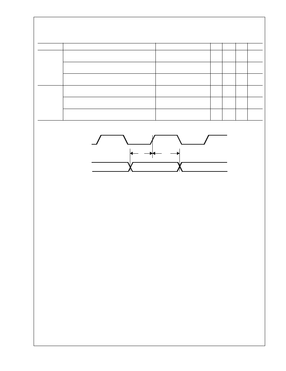
8.0 Electrical Specifications
(Continued)
75
Version A
DP83840A 10/100 Mb/s Ethernet Physical Layer
8.5 100 Mb/s AC Timing
8.5.1 100 Mb/s MII Transmit Timing
Parameter
Description
Notes
Min
Typ
Max
Units
T1
TXD[3:0], TX_EN, TX_ER Data Setup to
TX_CLK
100 Mb/s Translational
mode (Normal)
10
ns
TXD[4:0] Data Setup to TX_CLK
100 Mb/s Transparent
mode (BP_4B5B)
10
ns
TXD[4:0] Data Setup to TX_CLK
100 Mb/s Phaser mode
(BP_ALIGN)
10
ns
T2
TXD[3:0], TX_EN, TX_ER Data Hold from
TX_CLK
100 Mb/s Translational
mode (Normal)
-2
ns
TXD[4:0] Data Hold from TX_CLK
100 Mb/s Transparent
mode (BP_4B5B)
-2
ns
TXD[4:0] Data Hold from TX_CLK
100 Mb/s Phaser mode
(BP_ALIGN)
-2
ns
TX_CLK
TXD[3:0]
T1
T2
TX_EN
TX_ER
Valid Data
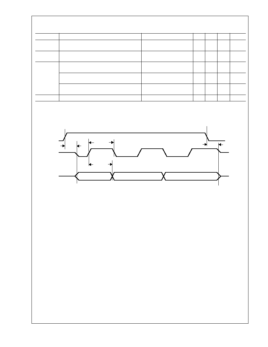
8.0 Electrical Specifications
(Continued)
76
Version A
DP83840A 10/100 Mb/s Ethernet Physical Layer
8.5.2 100 Mb/s MII Receive Timing
Note: RXD[3:0], RX_DV, and RX_ER are clocked out of the DP83840A on the falling edge of RX_CLK. However, in order to specify this parameter without
the RX_CLK duty cycle affecting it, the timing is taken from the previous rising edge of RX_CLK.
Parameter
Description
Notes
Min
Typ
Max
Units
T1
RX_EN to RX_CLK, RXD[3:0], RX_ER,
RX_DV Active
All 100 Mb/s modes
0
20
ns
T2
RX_EN to RX_CLK, RXD[3:0], RX_ER,
RX_DV Tri-State
All 100 Mb/s modes
0
30
ns
T3
RX_CLK to RXD[3:0], RX_DV, RX_ER Delay 100 Mb/s Translational
mode (Normal)
10
30
ns
RX_CLK to RXD[4:0], RX_DV, Delay
100 Mb/s Transparent mode
(BP_4B5B)
10
30
ns
RX_CLK to RXD[4:0], RX_DV, Delay
100 Mb/s Phaser mode
(BP_ALIGN), Note 2
10
30
ns
T4
RX_CLK Duty Cycle
All 100 Mb/s modes
35
65
%
RX_CLK
RXD[3:0]
RX_DV
RX_ER
Valid Data
RX_EN
T3
T1
T2
T4
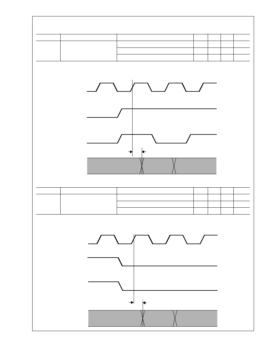
8.0 Electrical Specifications
(Continued)
77
Version A
DP83840A 10/100 Mb/s Ethernet Physical Layer
8.5.3 100 Mb/s Transmit Packet Timing
Parameter
Description
Notes
Min
Typ
Max
Units
T1
TX_CLK to TD+/- Latency
100 Mb/s Translational mode (Normal)
3.0
bits
100 Mb/s Transparent mode (BP_4B5B)
3.0
bits
100 Mb/s Phaser mode (BP_ALIGN)
3.0
bits
TX_CLK
TX_EN
TXD
TD+/-
T1
(J/K)
IDLE
DATA
8.5.4 100 Mb/s Transmit Packet Timing
Parameter
Description
Notes
Min
Typ
Max
Units
T1
TX_CLK to TD+/- deassertion 100 Mb/s Translational mode (Normal)
30
ns
100 Mb/s Transparent mode (BP_4B5B)
30
ns
100 Mb/s Phaser mode (BP_ALIGN)
30
ns
TX_CLK
TX_EN
TXD
TD+/-
T1
(T/R)
DATA
IDLE
Note: Latency is determined by measuring the time from the first rising edge of TX_CLK occurring after the assertion of TX_EN
to the first bit of the "j" code group as output from the TD+/- pins. 1 bit time = 10ns in 100 Mb/s mode
Note: De-assertion is determined by measuring the time from the first rising edge of TX_CLK occurring after the de-assertion of TX_EN
to the first bit of the "T" code group as output from the TD+/- pins. 1 bit time = 10ns in 100 Mb/s mode
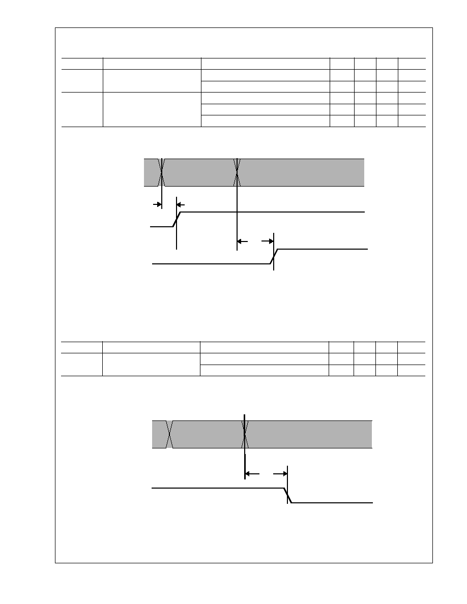
8.0 Electrical Specifications
(Continued)
78
Version A
DP83840A 10/100 Mb/s Ethernet Physical Layer
8.5.5 100 Mb/s Receive Packet Timing
Parameter
Description
Notes
Min
Typ
Max
Units
T1
Carrier Sense on Delay
100 Mb/s Translational mode (Normal)
175
ns
100 Mb/s Transparent mode (BP_4B5B)
175
ns
T2
Receive Data Latency
100 Mb/s Translational mode (Normal)
21
bits
100 Mb/s Transparent mode (BP_4B5B)
21
bits
100 Mb/s Phaser mode (BP_ALIGN)
10
bits
T2
T1
CRS
RXD[3:0]
RD+/-
RX_DV
RX_ER/RXD[4]
(J/K)
IDLE
Data
8.5.6 100 Mb/s Receive Packet Timing
Parameter
Description
Notes
Min
Typ
Max
Units
T1
Carrier Sense off Delay
100 Mb/s Translational mode (Normal)
135
ns
100 Mb/s Transparent mode (BP_4B5B)
135
ns
T1
CRS
RD+/-
(T/R)
IDLE
Data
Note: Carrier Sense Off Delay is determined by measuring the time from the first bit of the "IDLE" code group to the de-assertion of Carrier Sense.
1 bit time = 10ns in 10 Mb/s mode
Note: Carrier Sense On Delay is determined by measuring the time from the first bit of the "J" code group to the assertion of Carrier Sense.
1 bit time = 10ns in 100 Mb/s mode
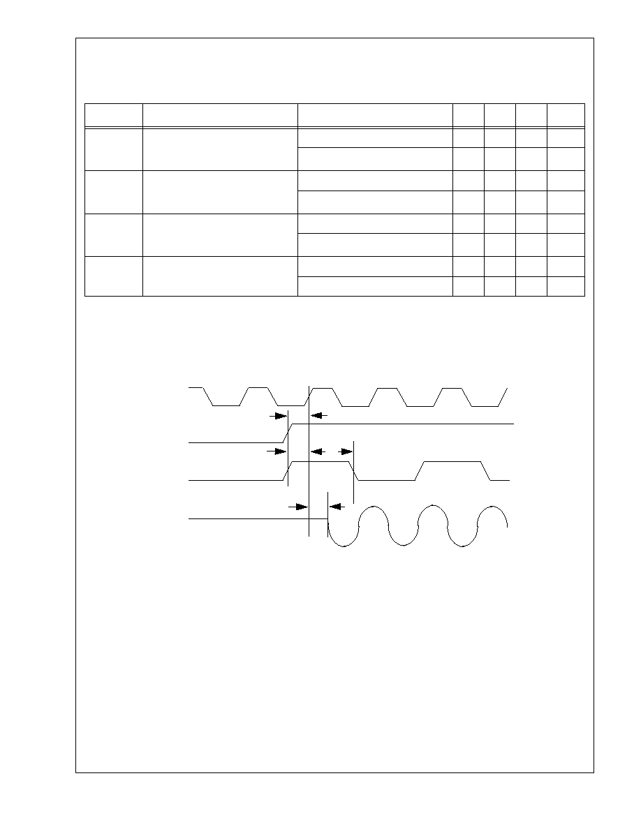
8.0 Electrical Specifications
(Continued)
79
Version A
DP83840A 10/100 Mb/s Ethernet Physical Layer
8.6 10 Mb/s AC Timing
8.6.1 10 Mb/s Transmit Timing (Start of Packet)
Parameter
Description
Notes
Min
Typ
Max
Units
T1
Transmit Enable Setup Time from
the Rising Edge of TXC
10 Mb/s nibble mode
20
ns
10 Mb/s serial mode
20
ns
T2
Transmit Data Setup Time from
the Rising Edge of TXC
10 Mb/s nibble mode
20
ns
10 Mb/s serial mode
20
ns
T3
Transmit Data Hold Time from the
Rising Edge of TXC
10 Mb/s nibble mode
-2
ns
10 Mb/s serial mode
-2
ns
T4
Transmit Latency (Rising Edge of
TXC to TXU+/-)
10 Mb/s nibble mode
6.8
bits
10 Mb/s serial mode
2.5
bits
TX_CLK
TX_EN
TXD
TXU+/-
TXS+/-
T1
T2
T3
T4
Note: 1 bit time = 100ns in 10 Mb/s mode for both nibble and serial operation.
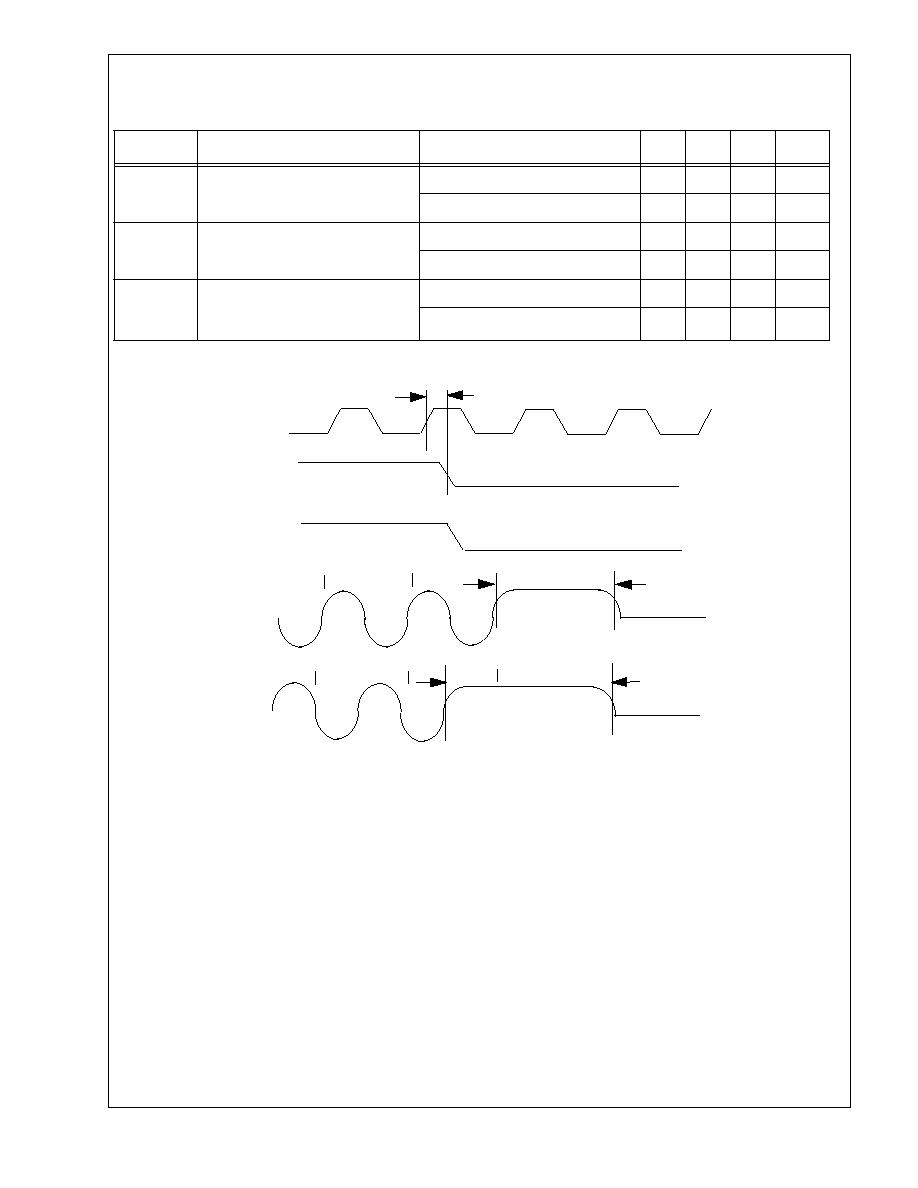
8.0 Electrical Specifications
(Continued)
80
Version A
DP83840A 10/100 Mb/s Ethernet Physical Layer
8.6.2 10 Mb/s Transmit Timing (End of Packet)
Parameter
Description
Notes
Min
Typ
Max
Units
T1
Transmit Enable Hold Time from
Rising Edge of TX_CLK
10 Mb/s nibble mode
-2
ns
10 Mb/s serial mode
-2
ns
T2
End of Packet High Time
(with `0' ending bit)
10 Mb/s nibble mode
250
ns
10 Mb/s serial mode
250
ns
T3
End of Packet High Time
(with `1' ending bit)
10 Mb/s nibble mode
250
ns
10 Mb/s serial mode
250
ns
TX_CLK
TX_EN
TXU+/-
TXS+/-
0
0
1
1
TXU+/-
TXS+/-
T1
T2
T3
TXD
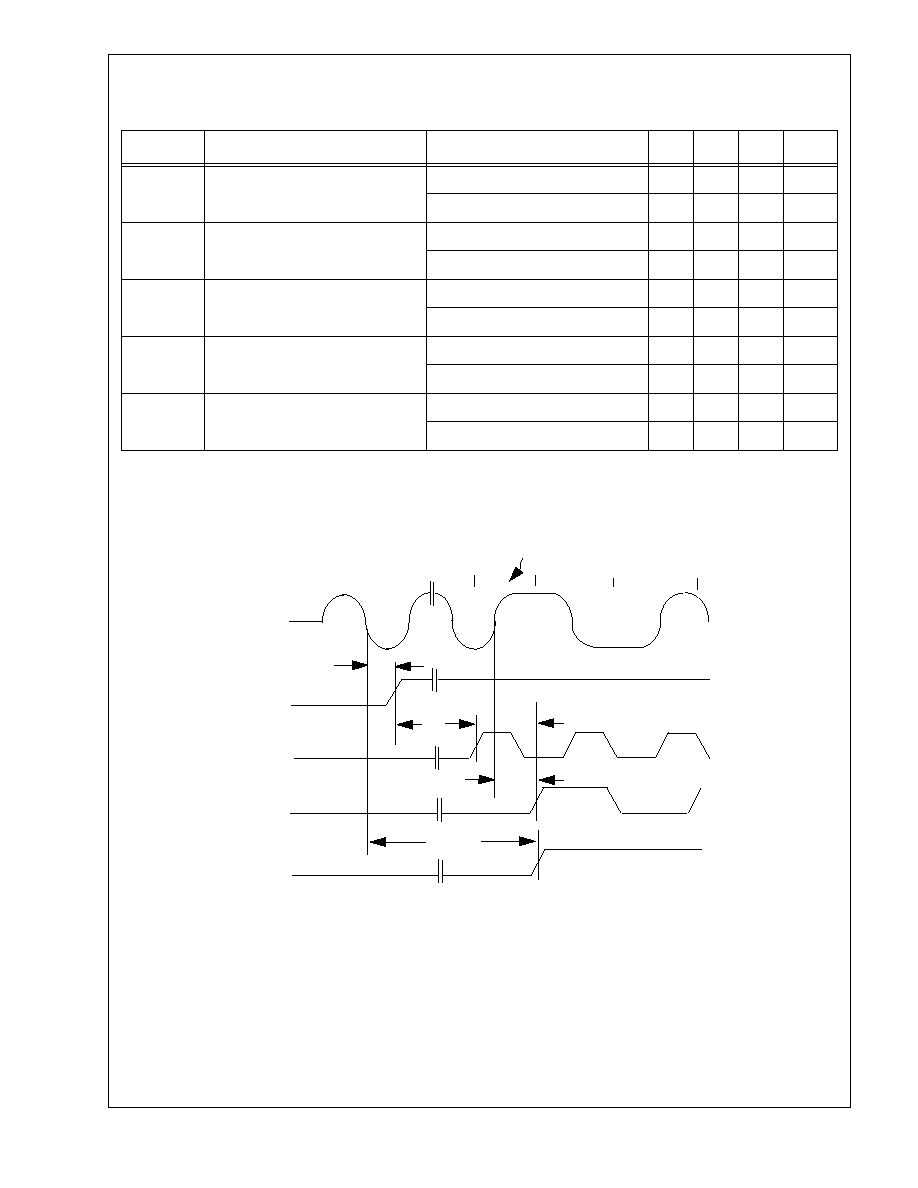
8.0 Electrical Specifications
(Continued)
81
Version A
DP83840A 10/100 Mb/s Ethernet Physical Layer
8.6.3 10 Mb/s Receive Timing (Start of Packet)
Parameter
Description
Notes
Min
Typ
Max
Units
T1
Carrier Sense Turn On Delay
(RXI+/- to CRS)
10 Mb/s nibble mode
1
µ
s
10 Mb/s serial mode
1
µ
s
T2
Decoder Acquisition Time
10 Mb/s nibble mode
2.6
µ
s
10 Mb/s serial mode
2.2
µ
s
T3
Receive Data Latency
10 Mb/s nibble mode
17.3
bits
10 Mb/s serial mode
10
bits
T4
SFD Latency
10 Mb/s nibble mode
10
bits
10 Mb/s serial mode
0.8
bits
T5
RX_CLK to RXD Delay Time
10 Mb/s nibble mode
-10
20
ns
10 Mb/s serial mode
-10
60
ns
1
0
1
T1
T2
T3
RXI+/-
CRS
RX_CLK
RXD
1st SFD bit decoded
Note: 10 Mb/s receive Data Latency is measured from first bit of preamble on the wire to the assertion of RX_DV
RX_DV
Note: 1 bit time = 100ns in 10 Mb/s mode for both nibble and serial operation.
T4
T5
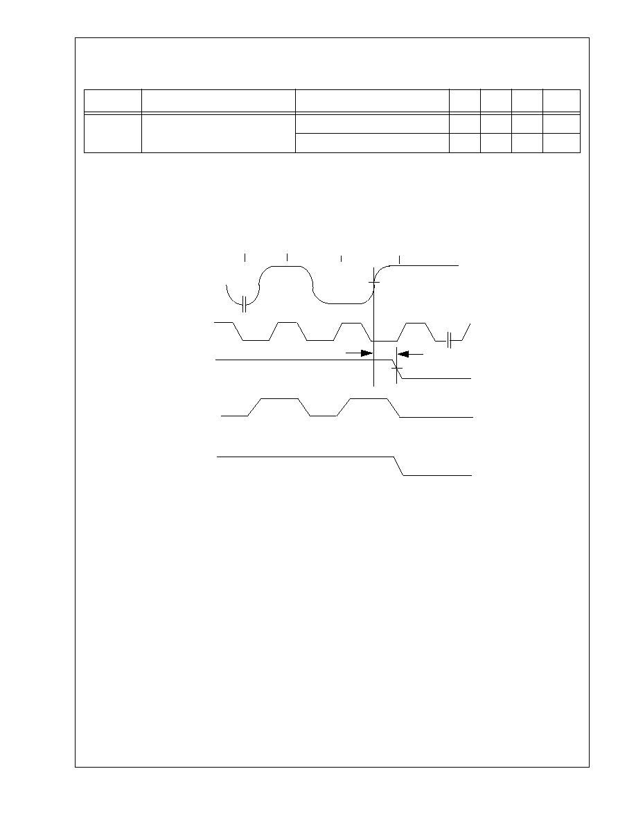
8.0 Electrical Specifications
(Continued)
82
Version A
DP83840A 10/100 Mb/s Ethernet Physical Layer
8.6.4 10 Mb/s Receive Timing (End of Packet)
Parameter
Description
Notes
Min
Typ
Max
Units
T1
Carrier Sense Turn Off Delay
10 Mb/s nibble mode
1.1
µ
s
10 Mb/s serial mode
150
ns
1
0
1
RXI+/-
RX_CLK
CRS
IDLE
T1
RXD
RX_DV
Note: The de-assertion of CRS is asynchronous and is therefore not directly measured.
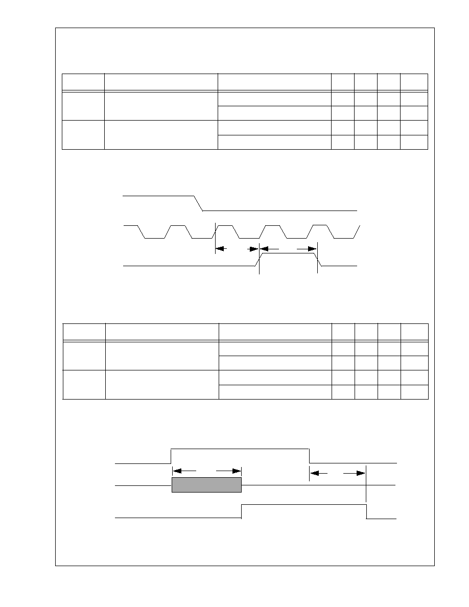
8.0 Electrical Specifications
(Continued)
83
Version A
DP83840A 10/100 Mb/s Ethernet Physical Layer
8.6.5 Heartbeat Timing
Parameter
Description
Notes
Min
Typ
Max
Units
T1
CD Heartbeat Delay
10 Mb/s nibble mode
1.6
µ
s
10 Mb/s serial mode
0.6
1.4
1.6
µ
s
T2
CD Heartbeat Duration
10 Mb/s nibble mode
1.3
µ
s
10 Mb/s serial mode
0.5
1.3
1.5
µ
s
TXC
TXE
COL
T1
T2
8.6.6 10 Mb/s Jabber Timing
Parameter
Description
Notes
Min
Typ
Max
Units
T1
Jabber Activation Time
10 Mb/s nibble mode
20
26
150
ms
10 Mb/s serial mode
20
26
150
ms
T2
Jabber Deactivation Time
10 Mb/s nibble mode
250
730
750
ms
10 Mb/s serial mode
250
730
750
ms
T1
T2
TXE
TD+/-
COL
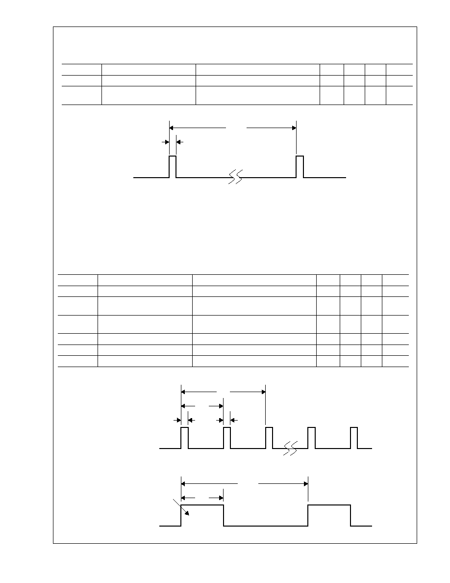
8.0 Electrical Specifications
(Continued)
84
Version A
DP83840A 10/100 Mb/s Ethernet Physical Layer
8.7 Auto-Negotiation Fast Link Pulse (FLP) Timing
8.7.1 Auto-Negotiation Fast Link Pulse (FLP) timing
Parameter
Description
Notes
Min
Typ
Max
Units
T1
Clock, Data Pulse Width
80
100
130
ns
T2
Clock Pulse to Clock Pulse
Period
111
125
139
µ
s
T3
Clock Pulse to Data Pulse
Period
Data = 1
55.5
69.5
µ
s
T4
Number of Pulses in a Burst
17
33
#
T5
Burst Width
2
ms
T6
FLP Burst to FLP Burst Period
8
24
ms
T2
T3
T1
T1
clock
pulse
data
pulse
clock
pulse
FLP Burst
FLP Burst
T6
T5
Fast Link Pulse(s)
T4
8.6.7 10BASE-T Normal Link Pulse Timing
Parameter
Description
Notes
Min
Typ
Max
Units
T1
Clock, Data Pulse Width
80
100
130
ns
T2
Clock Pulse to Clock Pulse
Period
8
16
24
ms
T2
T1
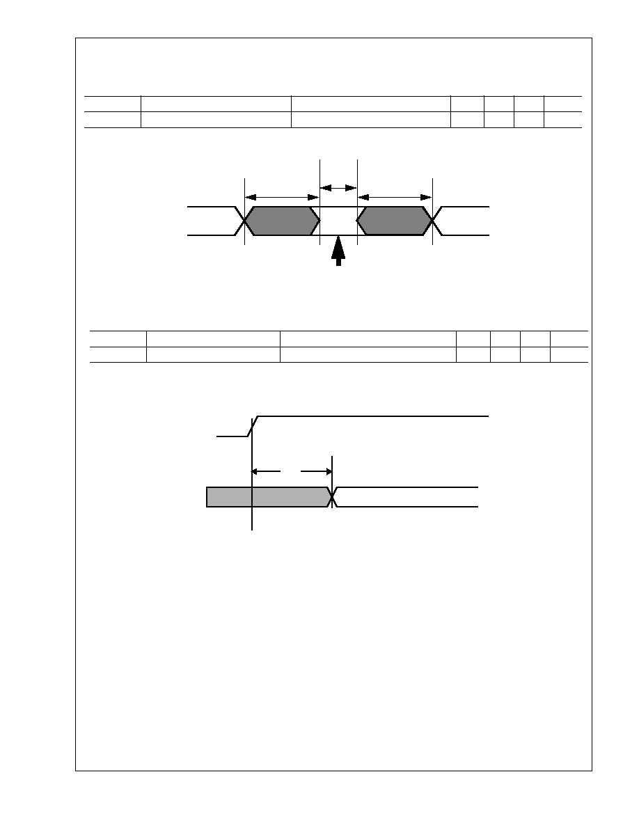
8.0 Electrical Specifications
(Continued)
85
Version A
DP83840A 10/100 Mb/s Ethernet Physical Layer
8.8 CRM (Clock Recovery Module) Timing
Note 1: The CRM Sampling Window is a measure of the PLL`s ability to recover data even with a high degree of jitter without error.
8.8.1 CRM Window Timing
Parameter
Description
Notes
Min
Typ
Max
Units
T1
CRM Sampling Window
(Note 1)
-1
1
ns
RD+/-
8.8.2 CRM Acquisition Time
Parameter
Description
Notes
Min
Typ
Max
Units
T1
CRM Acquisition
100 Mb/s
250
µ
s
SD
RD+/-
PLL Locked
T1
PLL Prior to Lock
Note: The Clock Generation Module (CGM) must be stable for at least 100
µ
s before the Clock Recovery Module (CRM) can lock to receive data.
3ns
3ns
JITTER
JITTER
CRM Sampling Point
T1
8.0 Electrical Specifications
(Continued)
86
Version A
DP83840A 10/100 Mb/s Ethernet Physical Layer
8.9 Reset Timing
Note: Software Reset should be initiated no sooner then 500
µ
s after power-up or the deassertion of hardware reset
.
Note: The timing for Hardware Reset Option 2 is equal to parameter T1 plus parameter T2 (501
µ
s total).
8.9.1 Hardware Reset Timing
Parameter
Description
Notes
Min
Typ
Max
Units
T1
Internal Reset Time
500
µ
s
T2
Hardware RESET Pulse Width
1
µ
s
T3
Post Reset Stabilization time
prior to MDC preamble for
register accesses
MDIO is pulled high for 32 bit serial
management initialization
500
µ
s
T4
Hardware Configuration Latch-
in Time from the Deassertion of
Reset (either soft or hard)
Hardware Configuration Pins are
described in section 3.10
800
ns
T5
Hardware Configuration pins
transition to output drivers
It is important to choose pull-up and/or
pull-down resistors for each of the
hardware configuration pins that provide
fast RC time constants in order to latch-in
the proper value prior to the pin
transitioning to an output driver
800
ns
T2
T1
Vcc
Hardware
Reset (option #1)
MDC
T3
32 clocks
Latch-In of Hardware
Configuration Pins
T4
Dual Function Pins
Become Enabled As Outputs
input
output
T5
Hardware
Reset (option #2)
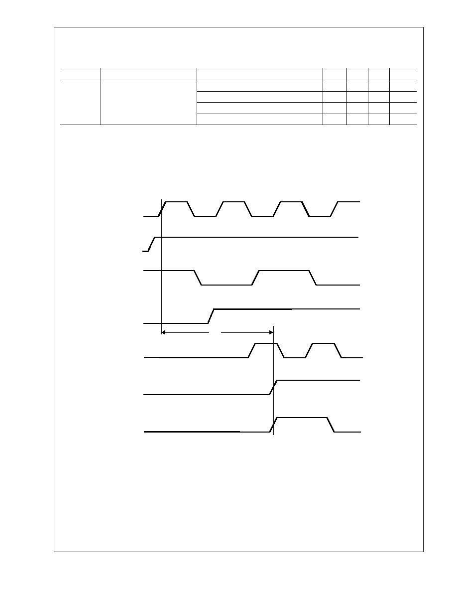
8.0 Electrical Specifications
(Continued)
87
Version A
DP83840A 10/100 Mb/s Ethernet Physical Layer
8.10 Loopback Timing
Note 1: The 100BASE-X PMD Loopback option timing is dependent on the external transceiver loopback timing and is therefore not defined herein.
Note 2: The TD+/- outputs of the DP83840A can be enabled or disabled during loopback operation via the LBK_XMT_DS bit (bit 5 of the LBREMR register).
Note 3: Due to the nature of the descrambler function, all 100BASE-X Loopback modes, with the exception of Remote Loopback, will cause an initial "dead-
time" of up to 750
µ
s during which time no data will be present at the receive MII outputs. The 100BASE-X timing shown here in section 6.3.16 is based on
device delays after the initial 750
µ
s "dead-time"
Note 4: During 10BASE-T loopback (serial or nibble mode) both the TXU+/- and TXS+/- outputs remain inactive.
8.10.1 10 Mb/s and 100 Mb/s Loopback Timing
Parameter
Description
Notes
Min
Typ
Max
Units
T1
TX_EN to RX_DV Loopback
100 Mb/s (note 1), (note2), (note3)
240
ns
10 Mb/s serial mode (note 4)
250
ns
10 Mb/s nibble mode (internal loopback)
2
µ
s
10 Mb/s nibble mode (normal operation)
2
µ
s
TX_CLK
TX_EN
TXD[3:0]
CRS
RX_CLK
RXD[3:0]
RX_DV
T1
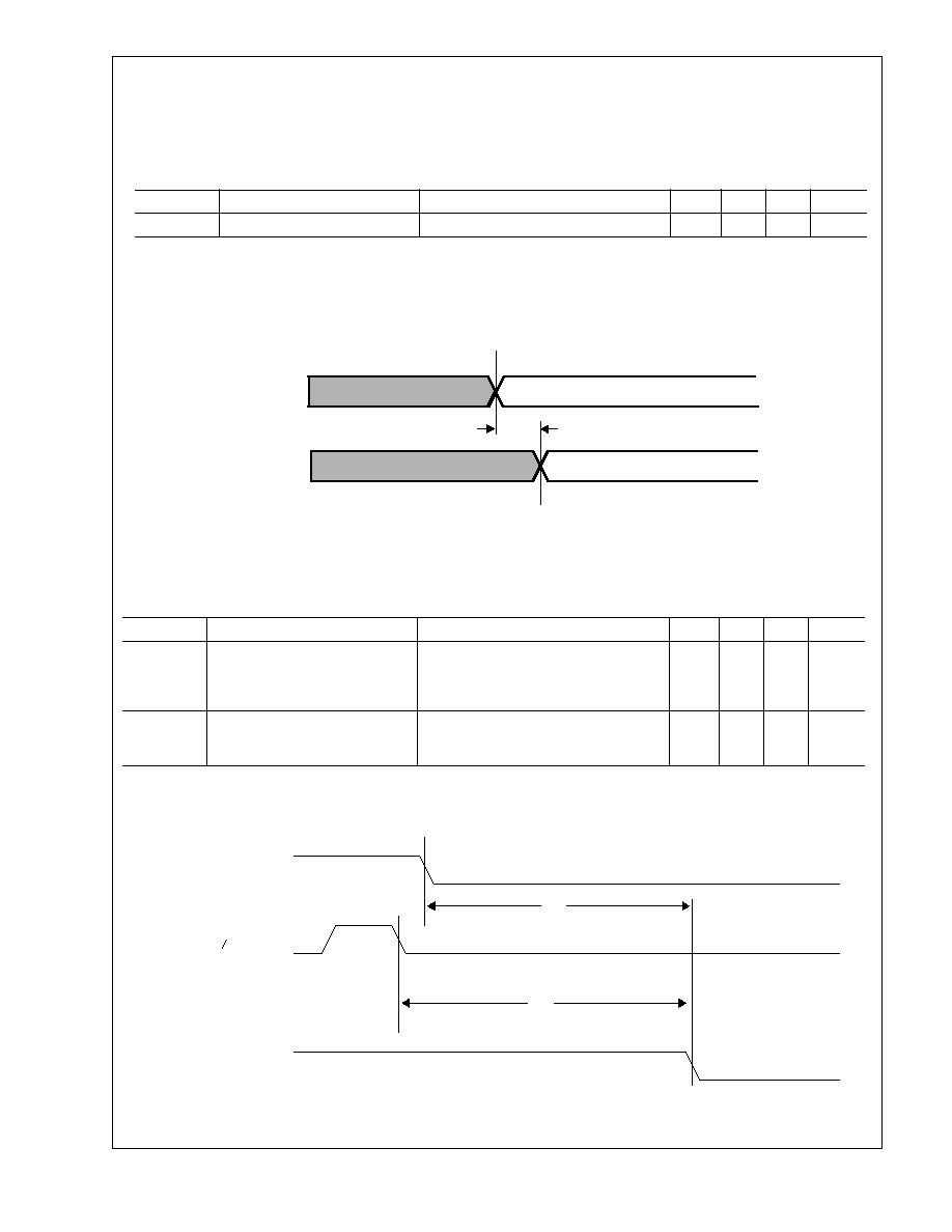
88
Version A
DP83840A 10/100 Mb/s Ethernet Physical Layer
8.0 Electrical Specifications
8.11 Isolation Timing
8.11.1 PHY Isolation Timing
Parameter
Description
Notes
Min
Typ
Max
Units
T1
From software clear of bit 10 in
the BMCR register to the
transition from Isolate to Normal
Mode
100
µ
s
T2
From Deassertion of S/W or H/W
Reset to transition from Isolate to
Normal mode
500
µ
s
Clear bit 10 of BMCR
(return to normal operation
from Isolate mode)
H/W or S/W Reset
(with PHYAD = 00000)
Mode
Isolate
Normal
T1
T2
RD+/-
Start of Packet
TD+/-
Start of Packet
IDLE
IDLE
T1
Remote Loopback Timing
8.10.2 Remote Loopback
Parameter
Description
Notes
Min
Typ
Max
Units
T1
Remote Loopback
100 Mb/s only
25
ns
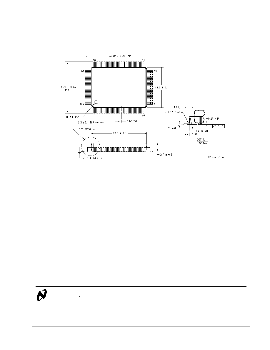
89
Version A
DP83840A 10/100 Mb/s Ethernet Physical Layer
7.0 Package Specification
LIFE SUPPORT POLICY
NATIONAL'S PRODUCTS ARE NOT AUTHORIZED FOR USE AS CRITICAL COMPONENTS IN LIFE SUPPORT
DEVICES OR SYSTEMS WITHOUT THE EXPRESS WRITTEN APPROVAL OF THE PRESIDENT OF NATIONAL
SEMICONDUCTOR CORPORATION. As used herein:
2. A critical component is any component of a life support
device or system whose failure to perform can be
reasonably expected to cause the failure of the life support
device or system, or to affect its safety or effectiveness.
1. Life support devices or systems we do or systems
which, (a) are intended for surgical implant into the
body, or (b) support or sustain life, and whose failure
to perform, when properly used in accordance with
instructions for use provided in the labeling, can be
reasonably expected to result in a significant injury to
the user.
National Semiconductor
Corporation
1111 West Bardin Road
Arlington, TX 76017
Tel: 1(800) 272-9959
Fax: 1(800) 737-7018
National Semiconductor
Corporation
Europe
Fax:(+49) 0-180-530 85 86
Email:cnjwge@tevm2.nsc.com
Duetsch Tel: (+49) 0-180-530 85 86
English Tel: (+49) 0-180-532 78 32
Francais Tel: (+49) 0-180-532 93 58
Italiano Tel: (+49) 0-180-534 16 80
National Semiconductor
Corporation
Japan Ltd.
Tel: 81-043-299-2308
Fax: 81-043-299-2408
National Semiconductor
Corporation
Hong Kong Ltd.
13th Floor, Straight Block,
Ocean Centre, 5 Canton Rd.
Tsimshatsui, Kowloon
Hong Kong
Tel: (852) 2737-1600
Fax: (852) 2736-9960
inches (millimeters)
100-Lead (14mm x 20mm) Molded Plastic Quad Flatpak, JEDEC
Order Number DP83840
NS Package Number VCE100A