DP83846A DsPHYTERÆ -- Single 10/100 Ethernet Transceiver
©
2000 National Semiconductor Corporation
www.national.com
Preliminary
April 2000
DP83846A DsPHYTER
Æ
-- Single 10/100 Ethernet Transceiver
General Description
The DP83846A is a full feature single Physical Layer
device with integrated PMD sublayers to support both
10BASE-T and 100BASE-TX Ethernet protocols over Cat-
egory 3 (10 Mb/s) or Category 5 unshielded twisted pair
cables.
The DP83846A is designed for easy implementation of
10/100 Mb/s Ethernet home or office solutions. It interfaces
to Twisted Pair media via an external transformer. This
device interfaces directly to MAC devices through the IEEE
802.3u standard Media Independent Interface (MII) ensur-
ing interoperability between products from different ven-
dors.
The DP83846A utilizes on chip Digital Signal Processing
(DSP) technology and digital Phase Lock Loops (PLLs) for
robust
performance
under
all
operating
conditions,
enhanced noise immunity, and lower external component
count when compared to analog solutions.
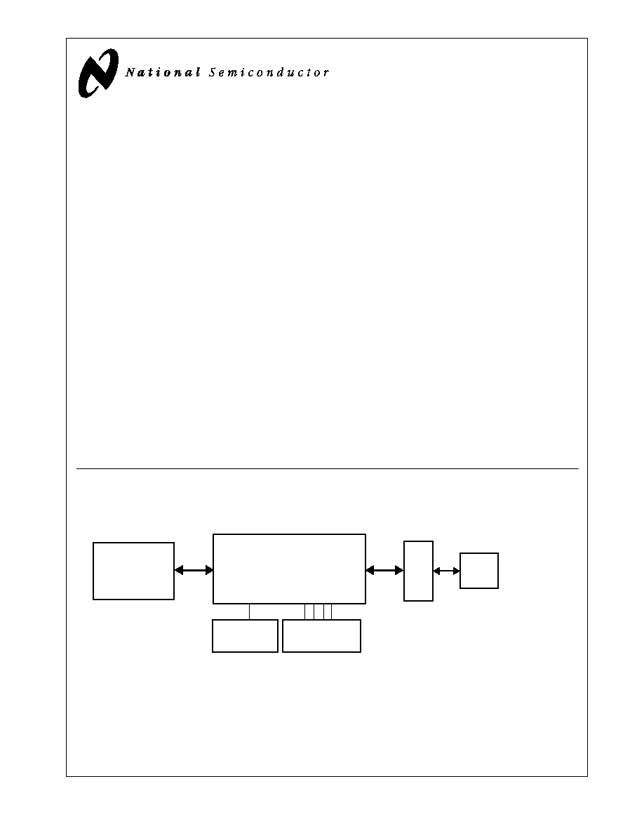
System Diagram
PHYTER
Æ
and TRI-STATE
Æ
are registered trademarks of National Semiconductor Corporation.
Status
10BASE-T
or
100BASE-TX
MII
25 MHz
Typical DsPHYTER application
Ethernet MAC
Magnetics
RJ-45
Clock
LEDs
DP83846A
10/100 Mb/s
DsPHYTER
Features
s
IEEE 802.3 ENDEC, 10BASE-T transceivers and filters
s
IEEE 802.3u PCS, 100BASE-TX transceivers and filters
s
IEEE 802.3 compliant Auto-Negotiation
s
Output edge rate control eliminates external filtering for
Transmit outputs
s
BaseLine Wander compensation
s
5V/3.3V MAC interface
s
IEEE 802.3u MII (16 pins/port)
s
LED support (Link, Rx, Tx, Duplex, Speed, Collision)
s
Single register access for complete PHY status
s
10/100 Mb/s packet loopback BIST (Built in Self Test)
s
Low-power 3.3V, 0.35um CMOS technology
s
5V tolerant I/Os
s
80-pin LQFP package (12w) x (12l) x (1.4h) mm
2
www.national.com
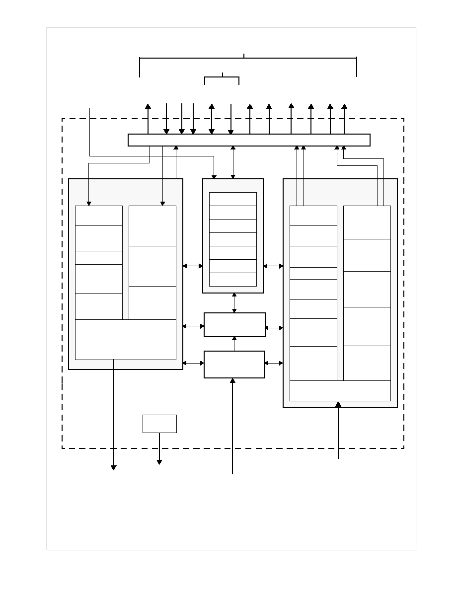
Figure 1. Block Diagram of the 10/100 DSP based core.
SERIAL
MANAGEMENT
MII
TX_CLK
TXD[3:0]
TX_ER
TX_EN
MDIO
MDC
COL
CRS
RX_ER
RX_D
V
RXD[3:0]
RX_CLK
TRANSMIT CHANNELS &
100 Mb/s
10 Mb/s
NRZ TO
MANCHESTER
ENCODER
STATE MACHINES
TRANSMIT
FILTER
LINK PULSE
GENERATOR
4B/5B
ENCODER
PARALLEL TO
SCRAMBLER
NRZ TO NRZI
ENCODER
BINARY TO
MLT-3
ENCODER
10/100 COMMON
RECEIVE CHANNELS &
100 Mb/s
10 Mb/s
MANCHESTER
TO NRZ
DECODER
STATE MACHINES
RECEIVE
FILTER
LINK PULSE
DETECTOR
4B/5B
DECODER
DESCRAMBLER
SERIAL TO
PARALLEL
NRZI TO NRZ
DECODER
MLT-3 TO
10/100 COMMON
AUTO-NEGOTIATION
STATE MACHINE
REGISTERS
AUTO
100BASE-TX
10BASE-T
MII
BASIC MODE
PCS CONTROL
PHY ADDRESS
NEGOTIATION
CLOCK
CLOCK
RECOVERY
CLOCK
RECOVERY
CODE GROUP
ALIGNMENT
SMART
SQUELCH
RX_DATA
RX_CLK
RX_DATA
RX_CLK
TX_DATA
TX_DATA
TX_CLK
SYSTEM CLOCK
REFERENCE
OUTPUT DRIVER
TD
INPUT BUFFER
BINARY
DECODER
ADAPTIVE
RD
LED
DRIVERS
LEDS
HARDWARE
CONFIGURATION
PINS
GENERATION
(AN_EN, AN0, AN1)
CONTROL
MII INTERFACE/CONTROL
(PAUSE_EN)
(LED_CFG, PHYAD)
SERIAL
BLW
AND EQ
COMP

3
www.national.com
Table of Contents
1.0
Pin Descriptions . . . . . . . . . . . . . . . . . . . . . . . . . . . . . . . 5
1.1
MII Interface . . . . . . . . . . . . . . . . . . . . . . . . . . . . . . 5
1.2
10 Mb/s and 100 Mb/s PMD Interface . . . . . . . . . . 6
1.3
Clock Interface . . . . . . . . . . . . . . . . . . . . . . . . . . . . 7
1.4
Special Connections . . . . . . . . . . . . . . . . . . . . . . . 7
1.5
LED Interface . . . . . . . . . . . . . . . . . . . . . . . . . . . . . 7
1.6
Strapping Options/Dual Purpose Pins . . . . . . . . . . 8
1.7
Reset . . . . . . . . . . . . . . . . . . . . . . . . . . . . . . . . . . . 9
1.8
Power and Ground Pins . . . . . . . . . . . . . . . . . . . . . 9
1.9
Package Pin Assignments . . . . . . . . . . . . . . . . . . 10
2.0
Configuration . . . . . . . . . . . . . . . . . . . . . . . . . . . . . . . 11
2.1
Auto-Negotiation . . . . . . . . . . . . . . . . . . . . . . . . . 11
2.2
PHY Address and LEDs . . . . . . . . . . . . . . . . . . . 12
2.3
LED INTERFACES . . . . . . . . . . . . . . . . . . . . . . . 13
2.4
Half Duplex vs. Full Duplex . . . . . . . . . . . . . . . . . 13
2.5
MII Isolate Mode . . . . . . . . . . . . . . . . . . . . . . . . . 14
2.6
Loopback . . . . . . . . . . . . . . . . . . . . . . . . . . . . . . . 14
2.7
BIST . . . . . . . . . . . . . . . . . . . . . . . . . . . . . . . . . . . 14
3.0
Functional Description . . . . . . . . . . . . . . . . . . . . . . . . 15
3.1
802.3u MII . . . . . . . . . . . . . . . . . . . . . . . . . . . . . . 15
3.2
100BASE-TX TRANSMITTER . . . . . . . . . . . . . . . 16
3.3
100BASE-TX RECEIVER . . . . . . . . . . . . . . . . . . 20
3.4
10BASE-T TRANSCEIVER MODULE . . . . . . . . . 23
3.5
TPI Network Circuit . . . . . . . . . . . . . . . . . . . . . . . 24
3.6
ESD Protection . . . . . . . . . . . . . . . . . . . . . . . . . . 25
3.7
Crystal Oscillator Circuit . . . . . . . . . . . . . . . . . . . 26
4.0
Reset Operation . . . . . . . . . . . . . . . . . . . . . . . . . . . . . . 26
4.1
Hardware Reset . . . . . . . . . . . . . . . . . . . . . . . . . . 26
4.2
Software Reset . . . . . . . . . . . . . . . . . . . . . . . . . . 26
5.0
Register Block . . . . . . . . . . . . . . . . . . . . . . . . . . . . . . . 27
5.1
Register Definition . . . . . . . . . . . . . . . . . . . . . . . . 29
5.2
Extended Registers . . . . . . . . . . . . . . . . . . . . . . . 37
6.0
Electrical Specifications . . . . . . . . . . . . . . . . . . . . . . . 44
6.1
DC Electrical Specification . . . . . . . . . . . . . . . . . . 44
6.2
PGM Clock Timing . . . . . . . . . . . . . . . . . . . . . . . 46
6.3
MII Serial Management Timing . . . . . . . . . . . . . . 46
6.4
100 Mb/s Timing . . . . . . . . . . . . . . . . . . . . . . . . . 47
6.5
10 Mb/s Timing . . . . . . . . . . . . . . . . . . . . . . . . . . 51
6.6
Reset Timing . . . . . . . . . . . . . . . . . . . . . . . . . . . . 56
6.7
Loopback Timing . . . . . . . . . . . . . . . . . . . . . . . . 57
6.8
Isolation Timing . . . . . . . . . . . . . . . . . . . . . . . . . . 58
7.0
Package Information . . . . . . . . . . . . . . . . . . . . . . . . . . 59
4
www.national.com
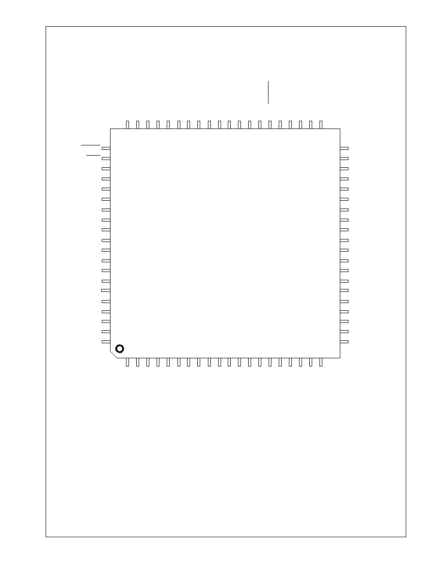
Connection Diagram
COL
TXD_3
TXD_2
IO_VDD
IO_GND
TXD_1
TXD_0
IO_GND
TX_EN
TX_CLK
TX_ER
CORE_VDD
CORE_GND
RESERVED
RX_ER/
PAUSE_EN
RX_CLK
RX_DV
IO_VDD
IO_GND
RXD_0
RESERVED
ANA_GND
RBIAS
ANA_VDD
RESERVED
ANA_GND
ANA_VDD
RESERVED
ANA_GND
RD-
RD+
ANA_VDD
ANA_GND
ANA_VDD
ANA_GND
TD+
TD-
ANA_GND
SUB_GND
RESERVED
DP83846A
DSPHYTER
1
2
3
4
5
6
7
8
9
10
11
12
13
14
15
16
17
18
19
20
61
62
63
64
65
66
67
68
69
70
71
72
73
74
75
76
77
78
79
80
60
59
58
57
56
55
54
53
52
51
50
49
48
47
46
45
44
43
42
41
40
39
38
37
36
35
34
33
32
31
30
29
28
27
26
25
24
23
22
21
CRS/LED_CFG
RESET
RESERVED
IO_GND
IO_VDD
X2
X1
RESERVED
RESERVED
RESERVED
RESERVED
CORE_VDD
CORE_GND
RESERVED
RESERVED
SUB_GND
RESERVED
RESERVED
SUB_GND
RESERVED
RXD_1
RXD_2
RXD_3
MDC
MDIO
IO_VDD
IO_GND
LED_DPLX/PHYAD0
LED_COL/PHYAD1
LED_GDLNK/PHYAD2
LED_TX/PHYAD3
LED_RX/PHYAD4
LED_SPEED
AN_EN
AN_1
AN_0
CORE_VDD
CORE_GND
RESERVED
RESERVED
Plastic Quad Flat Package JEDEC (LQFP)
Order Number DP83846AVHG
NS Package Number VHG80A

5
www.national.com
1.0 Pin Descriptions
The DP83846A pins are classified into the following inter-
face categories (each interface is described in the sections
that follow):
-- MII Interface
-- 10/100 Mb/s PMD Interface
-- Clock Interface
-- Special Connect Pins
-- LED Interface
-- Strapping Options/Dual Function pins
-- Reset
-- Power and Ground pins
Note: Strapping pin option (BOLD) Please see Section 1.6
for strap definitions.
All DP83846A signal pins are I/O cells regardless of the
particular use. Below definitions define the functionality of
the I/O cells for each pin.
1.1 MII Interface
Type: I
Inputs
Type: O
Outputs
Type: I/O
Input/Output
Type OD
Open Drain
Type: PD,PU Internal Pulldown/Pullup
Type: S
Strapping Pin (All strap pins except PHY-
AD[0:4] have internal pull-ups or pull-
downs. If the default strap value is needed
to be changed then an external 5 k
resistor
should be used. Please see Table 1.6 on
page 8 for details.)
Signal Name
Type
Pin #
Description
MDC
I
37
MANAGEMENT DATA CLOCK: Synchronous clock to the
MDIO management data input/output serial interface which
may be asynchronous to transmit and receive clocks. The
maximum clock rate is 25 MHz with no minimum clock rate.
MDIO
I/O, OD
36
MANAGEMENT DATA I/O: Bi-directional management in-
struction/data signal that may be sourced by the station
management entity or the PHY. This pin requires a 1.5 k
pullup resistor.
CRS/LED_CFG
O, S
61
CARRIER SENSE: Asserted high to indicate the presence
of carrier due to receive or transmit activity in 10BASE-T or
100BASE-TX Half Duplex Modes, while in full duplex mode
carrier sense is asserted to indicate the presence of carrier
due only to receive activity.
COL
O
60
COLLISION DETECT: Asserted high to indicate detection
of a collision condition (simultaneous transmit and receive
activity) in 10 Mb/s and 100 Mb/s Half Duplex Modes.
While in 10BASE-T Half Duplex mode with Heartbeat en-
abled this pin are also asserted for a duration of approxi-
mately 1
µ
s at the end of transmission to indicate heartbeat
(SQE test).
In Full Duplex Mode, for 10 Mb/s or 100 Mb/s operation, this
signal is always logic 0. There is no heartbeat function dur-
ing 10 Mb/s full duplex operation.
TX_CLK
O
51
TRANSMIT CLOCK: 25 MHz Transmit clock outputs in
100BASE-TX mode or 2.5 MHz in 10BASE-T mode derived
from the 25 MHz reference clock.
TXD[3]
TXD[2]
TXD[1]
TXD[0]]
I
59, 58, 55,
54
TRANSMIT DATA: Transmit data MII input pins that accept
nibble data synchronous to the TX_CLK (2.5 MHz in
10BASE-T Mode or 25 MHz in 100BASE-TX mode).
TX_EN
I
52
TRANSMIT ENABLE: Active high input indicates the pres-
ence of valid nibble data on data inputs, TXD[3:0] for both
100 Mb/s or 10 Mb/s nibble mode.
TX_ER
I
50
TRANSMIT ERROR: In 100MB/s mode, when this signal is
high and the corresponding TX_EN is active the HALT sym-
bol is substituted for data.
In 10 Mb/s this input is ignored.