 | –≠–ª–µ–∫—Ç—Ä–æ–Ω–Ω—ã–π –∫–æ–º–ø–æ–Ω–µ–Ω—Ç: DP83847 | –°–∫–∞—á–∞—Ç—å:  PDF PDF  ZIP ZIP |
D
P
8
3
8
47
Ds
PH
YTE
R
II --
Single
10
/10
0
E
t
he
rnet
Tra
n
sc
eiv
e
r
©
2002 National Semiconductor Corporation
www.national.com
February 2002
DP83847 DsPHYTER II -- Single 10/100 Ethernet Transceiver
General Description
The DP83847 is a full feature single Physical Layer device
with integrated PMD sublayers to support both 10BASE-T
and 100BASE-TX Ethernet protocols over Category 3 (10
Mb/s) or Category 5 unshielded twisted pair cables.
The DP83847 is designed for easy implementation of
10/100 Mb/s Ethernet home or office solutions. It interfaces
to Twisted Pair media via an external transformer. This
device interfaces directly to MAC devices through the IEEE
802.3u standard Media Independent Interface (MII) ensur-
ing interoperability between products from different ven-
dors.
The DP83847 utilizes on chip Digital Signal Processing
(DSP) technology and digital Phase Lock Loops (PLLs) for
robust performance under all operating conditions,
enhanced noise immunity, and lower external component
count when compared to analog solutions.
Applications
s
LAN on Motherboard
s
Embedded Applications
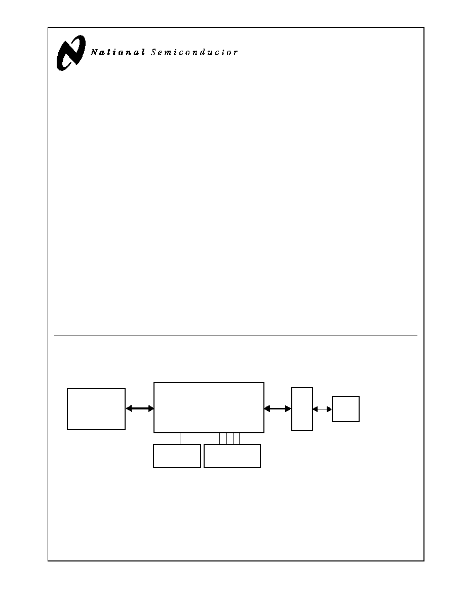
System Diagram
Status
10BASE-T
or
100BASE-TX
MII
25 MHz
Typical DsPHYTER II application
Ethernet MAC
Magnet
ics
RJ-45
Clock
LEDs
DP83847
10/100 Mb/s
DsPHYTER II
Features
s
Low-power 3.3V, 0.18
µ
m CMOS technology
s
Power consumption < 351mW (typical)
s
5V tolerant I/Os
s
5V/3.3V MAC interface
s
IEEE 802.3 ENDEC, 10BASE-T transceivers and filters
s
IEEE 802.3u PCS, 100BASE-TX transceivers and filters
s
IEEE 802.3 compliant Auto-Negotiation
s
Output edge rate control eliminates external filtering for
Transmit outputs
s
BaseLine Wander compensation
s
IEEE 802.3u MII (16 pins/port)
s
LED support (Link, Rx, Tx, Duplex, Speed, Collision)
s
Single register access for complete PHY status
s
10/100 Mb/s packet loopback BIST (Built in Self Test)
s
56-pin LLP package (9w) x (9l) x (.75h) mm
2
www.national.com
DP
83
84
7
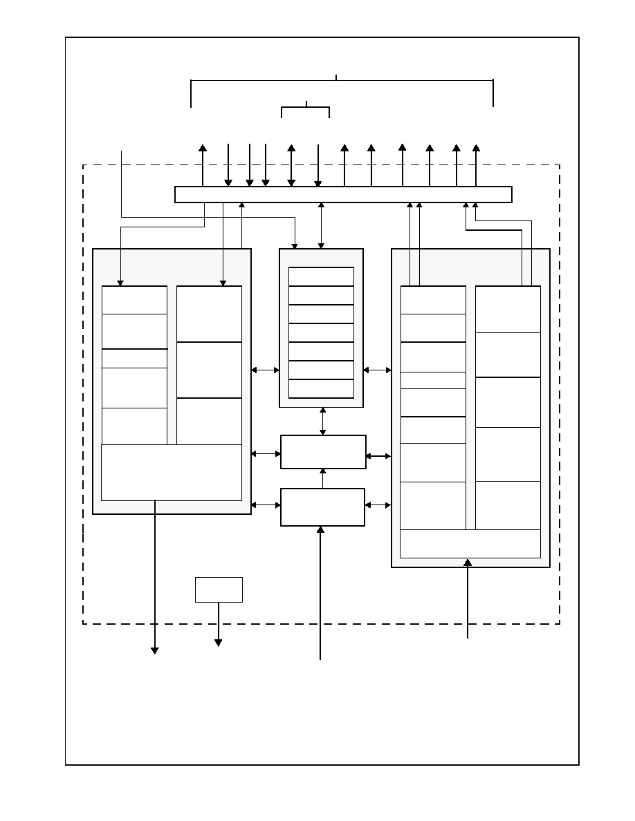
Figure 1. Block Diagram of the 10/100 DSP based core.
SERIAL
MANAGEMENT
MII
TX
_
C
LK
T
X
D[3:0]
TX_
E
R
TX_
E
N
MD
I
O
MD
C
COL
CRS
RX
_
E
R
RX
_DV
RXD
[
3:0]
RX
_CLK
TRANSMIT CHANNELS &
100 Mb/s
10 Mb/s
NRZ TO
MANCHESTER
ENCODER
STATE MACHINES
TRANSMIT
FILTER
LINK PULSE
GENERATOR
4B/5B
ENCODER
PARALLEL TO
SCRAMBLER
NRZ TO NRZI
ENCODER
BINARY TO
MLT-3
ENCODER
10/100 COMMON
RECEIVE CHANNELS &
100 Mb/s
10 Mb/s
MANCHESTER
TO NRZ
DECODER
STATE MACHINES
RECEIVE
FILTER
LINK PULSE
DETECTOR
4B/5B
DECODER
DESCRAMBLER
SERIAL TO
PARALLEL
NRZI TO NRZ
DECODER
MLT-3 TO
10/100 COMMON
AUTO-NEGOTIATION
STATE MACHINE
REGISTERS
AUTO
100BASE-TX
10BASE-T
MII
BASIC MODE
PCS CONTROL
PHY ADDRESS
NEGOTIATION
CLOCK
CLOCK
RECOVERY
CLOCK
RECOVERY
CODE GROUP
ALIGNMENT
SMART
SQUELCH
RX_DATA
RX_CLK
RX_DATA
RX_CLK
TX_DATA
TX_DATA
TX_CLK
SYSTEM CLOCK
REFERENCE
OUTPUT DRIVER
TD±
INPUT BUFFER
BINARY
DECODER
ADAPTIVE
RD±
LED
DRIVERS
LEDS
HARDWARE
CONFIGURATION
PINS
GENERATION
(AN_EN, AN0, AN1)
CONTROL
MII INTERFACE/CONTROL
(PAUSE_EN)
(LED_CFG, PHYAD)
SERIAL
BLW
AND EQ
COMP

3
www.national.com
DP
83
84
7
Table of Content
1.0
Pin Descriptions . . . . . . . . . . . . . . . . . . . . . . . . . . . . . . . 5
1.1
MII Interface . . . . . . . . . . . . . . . . . . . . . . . . . . . . . . 5
1.2
10 Mb/s and 100 Mb/s PMD Interface . . . . . . . . . . 6
1.3
Clock Interface . . . . . . . . . . . . . . . . . . . . . . . . . . . . 7
1.4
Special Connections . . . . . . . . . . . . . . . . . . . . . . . 7
1.5
LED Interface . . . . . . . . . . . . . . . . . . . . . . . . . . . . . 7
1.6
Strapping Options/Dual Purpose Pins . . . . . . . . . . 8
1.7
Reset . . . . . . . . . . . . . . . . . . . . . . . . . . . . . . . . . . . 9
1.8
Power and Ground Pin . . . . . . . . . . . . . . . . . . . . . 9
1.9
Package Pin Assignments . . . . . . . . . . . . . . . . . . 10
2.0
Configuration . . . . . . . . . . . . . . . . . . . . . . . . . . . . . . . . 11
2.1
Auto-Negotiation . . . . . . . . . . . . . . . . . . . . . . . . . 11
2.2
PHY Address and LEDs . . . . . . . . . . . . . . . . . . . 12
2.3
LED INTERFACES . . . . . . . . . . . . . . . . . . . . . . . 13
2.4
Half Duplex vs. Full Duplex . . . . . . . . . . . . . . . . . 13
2.5
MII Isolate Mode . . . . . . . . . . . . . . . . . . . . . . . . . 14
2.6
Loopback . . . . . . . . . . . . . . . . . . . . . . . . . . . . . . . 14
2.7
BIST . . . . . . . . . . . . . . . . . . . . . . . . . . . . . . . . . . . 14
3.0
Functional Description . . . . . . . . . . . . . . . . . . . . . . . . . 15
3.1
802.3u MII . . . . . . . . . . . . . . . . . . . . . . . . . . . . . . 15
3.2
100BASE-TX TRANSMITTER . . . . . . . . . . . . . . . 16
3.3
100BASE-TX RECEIVER . . . . . . . . . . . . . . . . . . 20
3.4
10BASE-T TRANSCEIVER MODULE . . . . . . . . . 23
3.5
TPI Network Circuit . . . . . . . . . . . . . . . . . . . . . . . 24
3.6
ESD Protection . . . . . . . . . . . . . . . . . . . . . . . . . . 25
3.7
Crystal Oscillator Circuit . . . . . . . . . . . . . . . . . . . 26
3.8
Reference Bypass Couple . . . . . . . . . . . . . . . . . . 26
4.0
Reset Operation . . . . . . . . . . . . . . . . . . . . . . . . . . . . . . 26
4.1
Hardware Reset . . . . . . . . . . . . . . . . . . . . . . . . . . 26
4.2
Software Reset . . . . . . . . . . . . . . . . . . . . . . . . . . 26
5.0
Register Block . . . . . . . . . . . . . . . . . . . . . . . . . . . . . . . 27
5.1
Register Definition . . . . . . . . . . . . . . . . . . . . . . . . 29
5.2
Extended Registers . . . . . . . . . . . . . . . . . . . . . . . 37
6.0
Electrical Specifications . . . . . . . . . . . . . . . . . . . . . . . 44
6.1
Reset Timing . . . . . . . . . . . . . . . . . . . . . . . . . . . . 46
6.2
PGM Clock Timing . . . . . . . . . . . . . . . . . . . . . . . 47
6.3
MII Serial Management Timing . . . . . . . . . . . . . . 47
6.4
100 Mb/s Timing . . . . . . . . . . . . . . . . . . . . . . . . . 48
6.5
10 Mb/s Timing . . . . . . . . . . . . . . . . . . . . . . . . . . 52
6.6
Loopback Timing . . . . . . . . . . . . . . . . . . . . . . . . . 57
6.7
Isolation Timing . . . . . . . . . . . . . . . . . . . . . . . . . . 59
7.0
Physical Dimensions . . . . . . . . . . . . . . . . . . . . . . . . 60
4
www.national.com
DP
83
84
7
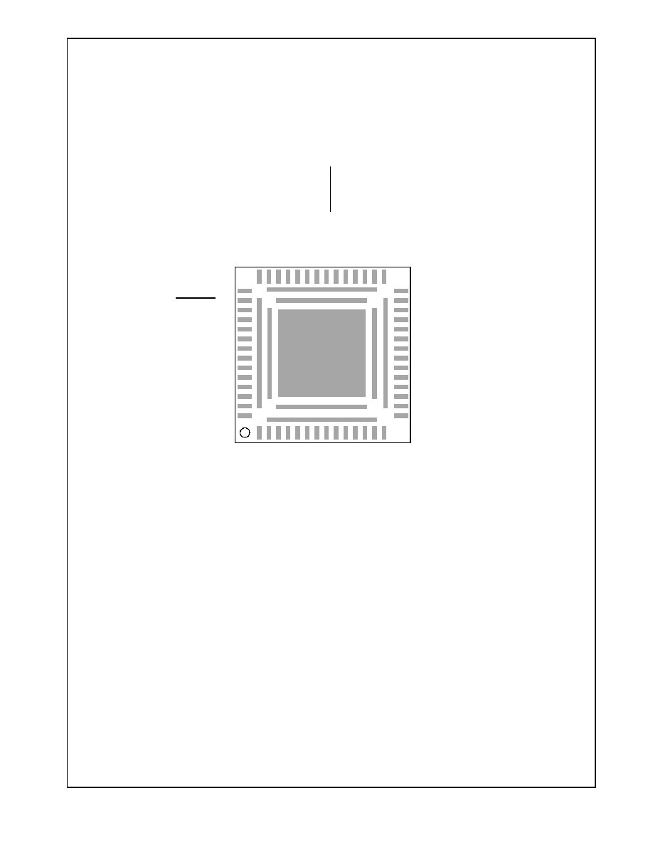
Pin Layout
28 VDD
27 RXD_2
26 RXD_3
25 MDC
24 MDIO
23 LED_DPLX/PHYAD0
22 LED_COL/PHYAD1
21 LED_GDLNK/PHYAD2
20 LED_TX/PHYAD3
19 LED_RX/PHYAD4
18 LED_SPEED
17 AN_EN
16 AN_1
15 AN_0
COL 43
RESERVED 44
CRS/LED_CFG 45
RESET 46
RESERVED 47
X2 48
X1 49
RESERVED 50
RESERVED 51
RESERVED 52
RESERVED 53
RESERVED 54
RESERVED 55
VDD 56
42 C1
41 T
X
D_3
40 T
X
D_2
39 T
X
D_1
38 T
X
D_0
37 T
X
_E
N
36 T
X
_CLK
35 T
X
_E
R
34 RE
SER
V
E
D
33 RX
_E
R/P
A
US
E
_
E
N
32 RX
_CLK
31 RX
_DV
30 RX
D_0
29 RX
D_1
R
ESE
R
V
E
D
1
R
ESE
R
V
E
D
2
RB
IA
S
3
R
ESE
R
V
E
D
4
R
ESE
R
V
E
D
5
RD -
6
RD+ 7
R
ESE
R
V
E
D
8
R
ESE
R
V
E
D
9
TD+ 1
0
TD
-
1
1
RE
S
E
R
V
E
D
12
RE
S
E
R
V
E
D
13
VD
D
14
Top View
Leadless Leadframe Package (LLP)
Order Number DP83847ALQA56A
NS Package Number LQA-56A
65 Gnd
57
58
63
64
61
62
59
60
Note 1: Pins 57 to 65 required soldering care. Check Package Instruction, AN-1187, for details.

5
www.national.com
DP
83
84
7
1.0 Pin Descriptions
The DP83847 pins are classified into the following interface
categories (each interface is described in the sections that
follow):
-- MII Interface
-- 10/100 Mb/s PMD Interface
-- Clock Interface
-- Special Connect Pins
-- LED Interface
-- Strapping Options/Dual Function pins
-- Reset
-- Power and Ground pins
Note: Strapping pin option (BOLD) Please see Section 1.6
for strap definitions.
All DP83847 signal pins are I/O cells regardless of the par-
ticular use. Below definitions define the functionality of the
I/O cells for each pin.
1.1 MII Interface
Type: I
Inputs
Type: O
Outputs
Type: I/O
Input/Output
Type OD
Open Drain
Type: PD,PU Internal Pulldown/Pullup
Type: S
Strapping Pin (All strap pins except PHY-
AD[0:4] have internal pull-ups or pull-
downs. If the default strap value is needed
to be changed then an external 5 k
resistor
should be used. Please see Table 1.6 on
page 8 for details.)
Signal Name
Type
LLP Pin #
Description
MDC
I
25
MANAGEMENT DATA CLOCK: Synchronous clock to the MDIO
management data input/output serial interface which may be
asynchronous to transmit and receive clocks. The maximum clock
rate is 25 MHz with no minimum clock rate.
MDIO
I/O, OD
24
MANAGEMENT DATA I/O: Bi-directional management instruc-
tion/data signal that may be sourced by the station management
entity or the PHY. This pin requires a 1.5 k
pullup resistor.
CRS/LED_CFG
O, S
45
CARRIER SENSE: Asserted high to indicate the presence of car-
rier due to receive or transmit activity in 10BASE-T or 100BASE-
TX Half Duplex Modes, while in full duplex mode carrier sense is
asserted to indicate the presence of carrier due only to receive ac-
tivity.
COL
O
43
COLLISION DETECT: Asserted high to indicate detection of a
collision condition (simultaneous transmit and receive activity) in
10 Mb/s and 100 Mb/s Half Duplex Modes.
While in 10BASE-T Half Duplex mode with Heartbeat enabled this
pin are also asserted for a duration of approximately 1
µ
s at the
end of transmission to indicate heartbeat (SQE test).
In Full Duplex Mode, for 10 Mb/s or 100 Mb/s operation, this sig-
nal is always logic 0. There is no heartbeat function during 10
Mb/s full duplex operation.
TX_CLK
O
36
TRANSMIT CLOCK: 25 MHz Transmit clock outputs in
100BASE-TX mode or 2.5 MHz in 10BASE-T mode derived from
the 25 MHz reference clock.
TXD[3]
TXD[2]
TXD[1]
TXD[0]]
I
41, 40, 39,
38
TRANSMIT DATA: Transmit data MII input pins that accept nib-
ble data synchronous to the TX_CLK (2.5 MHz in 10BASE-T
Mode or 25 MHz in 100BASE-TX mode).
TX_EN
I
37
TRANSMIT ENABLE: Active high input indicates the presence of
valid nibble data on data inputs, TXD[3:0] for both 100 Mb/s or 10
Mb/s nibble mode.
TX_ER
I
35
TRANSMIT ERROR: In 100MB/s mode, when this signal is high
and the corresponding TX_EN is active the HALT symbol is sub-
stituted for data.
In 10 Mb/s this input is ignored.
RX_CLK
O, PU
32
RECEIVE CLOCK: Provides the 25 MHz recovered receive
clocks for 100BASE-TX mode and 2.5 MHz for 10BASE-T nibble
mode.