D
P
8
3
8
61
EN
Gig
PH
YTER
Æ
10
/10
0
/1
00
0 E
t
he
rnet
Phy
s
ic
al
Lay
e
r
©
2001 National Semiconductor Corporation
www.national.com
General Description
The DP83861 is a full featured Physical Layer transceiver
with integrated PMD sublayers to support 10BASE-T,
100BASE-TX and 1000BASE-T Ethernet protocols.
The DP83861 uses state of the art 0.18
µ
m
,
1.8 V/3.3 V
CMOS technology, fabricated at National Semiconductor's
South Portland Maine facility.
The DP83861 is designed for easy implementation of
10/100/1000 Mb/s Ethernet LANs. It interfaces directly to
Twisted Pair media via an external transformer. This device
interfaces directly to the MAC layer through the IEEE
802.3u Standard Media Independent Interface (MII) or the
IEEE 802.3z Gigabit Media Independent Interface (GMII).
Applications
The DP83861 fits applications in:
s
10/100/1000 Mb/s capable node cards
s
Switches with 10/100/1000 Mb/s capable ports
s
High speed uplink ports (backbone)
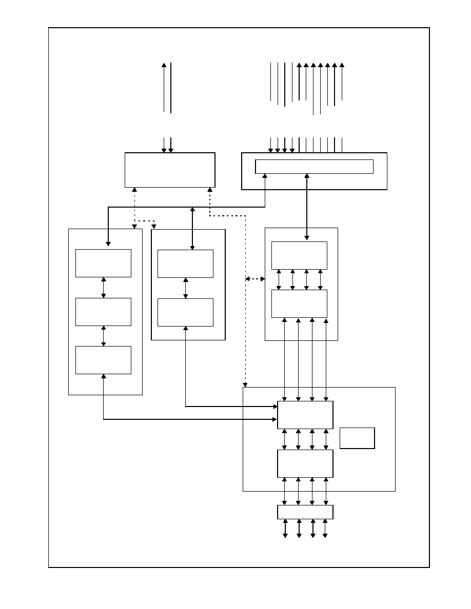
System Diagram
ETHERNET
DP83861
STATUS
LEDs
M
A
G
N
ETI
C
S
RJ-45
100BASE-TX
MII/GMII
MAC
CLOCK
125 MHz or 25 MHz
1000BASE-T
DP83820
10BASE-T
10/100/1000Mb/s
10/100/1000Mb/s
Ethernet Physical Layer
Features
s
100BASE-TX and 1000BASE-T compliant
s
Fully compliant to IEEE 802.3u 100BASE-TX and IEEE
802.3z/ab 1000BASE-T specifications. Fully integrated
and fully compliant ANSI X3.T12 PMD physical sublayer
that includes adaptive equalization and Baseline Wan-
der compensation
s
10BASE-T compatible
s
IEEE 802.3u Auto-Negotiation and Parallel Detection
≠ Fully Auto-Negotiates between 1000 Mb/s, 100 Mb/s,
and 10 Mb/s Full Duplex and Half Duplex devices
s
Interoperates with first generation 1000BASE-T Physical
layer transceivers
s
3.3V MAC interfaces:
≠ IEEE 802.3u MII
≠ IEEE 802.3z GMII
s
LED support: Link, Speed, Activity, Collision, TX and RX
s
Supports 125 MHz or 25 MHz reference clock
s
Requires only one 1.8 V and one 3.3 V supply
s
Supports MDIX at 10, 100, and 1000 Mb/s
s
Supports JTAG (IEEE1149.1)
s
Dissipates 1 watt in 10/100 Mb/s mode
s
Programmable Interrupts
s
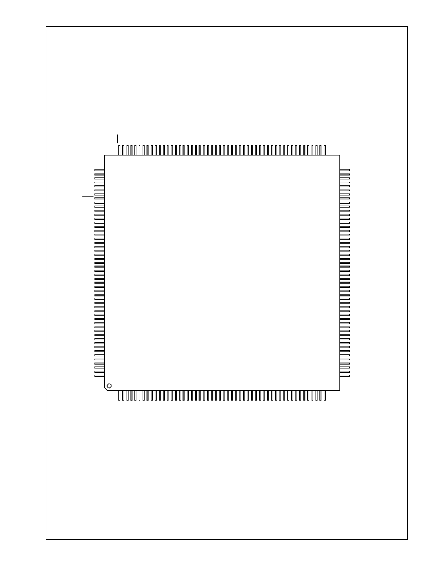
208-pin PQFP package
DP83861VQM-3 EN Gig PHYTER
Æ
10/100/1000 Ethernet Physical Layer
PRELIMINARY
April 2001
PHYTER
Æ
is a registered trademark of National Semiconductor Corporation.

3
www.national.com
Table of Contents
DP838
61
1.0
Pin Descriptions . . . . . . . . . . . . . . . . . . . . . . . . . . . . . . . 5
1.1
MAC Interface . . . . . . . . . . . . . . . . . . . . . . . . . . . . 5
1.2
TP Interface . . . . . . . . . . . . . . . . . . . . . . . . . . . . . . 6
1.3
JTAG Interface . . . . . . . . . . . . . . . . . . . . . . . . . . . . 7
1.4
E2PROM Interface . . . . . . . . . . . . . . . . . . . . . . . . . 8
1.5
Clock Interface . . . . . . . . . . . . . . . . . . . . . . . . . . . . 8
1.6
LED/Interrupt Interface . . . . . . . . . . . . . . . . . . . . . 8
1.7
Device Configuration Interface . . . . . . . . . . . . . . . 9
1.8
Reset . . . . . . . . . . . . . . . . . . . . . . . . . . . . . . . . . . 10
1.9
Power And Ground Pins . . . . . . . . . . . . . . . . . . . 10
1.10
Special Connect Pins . . . . . . . . . . . . . . . . . . . . . . 11
2.0
Configuration . . . . . . . . . . . . . . . . . . . . . . . . . . . . . . . . 12
2.1
Speed/Duplex Mode Selection . . . . . . . . . . . . . . 12
2.2
Manual Mode Configurations . . . . . . . . . . . . . . . . 12
2.3
Auto-Negotiation . . . . . . . . . . . . . . . . . . . . . . . . . 13
2.4
MII Isolate Mode . . . . . . . . . . . . . . . . . . . . . . . . . 15
2.5
Loopback . . . . . . . . . . . . . . . . . . . . . . . . . . . . . . . 15
2.6
MII/GMII Interface and Speed of Operation . . . . . 15
2.7
Test Modes . . . . . . . . . . . . . . . . . . . . . . . . . . . . . 16
2.8
Automatic MDI / MDI-X Configuration . . . . . . . . . 16
2.9
Polarity Correction . . . . . . . . . . . . . . . . . . . . . . . . 16
2.10
Firmware Interrupt . . . . . . . . . . . . . . . . . . . . . . . . 16
3.0
Design and Layout Guide . . . . . . . . . . . . . . . . . . . . . . 17
3.1
Power Supply Filtering . . . . . . . . . . . . . . . . . . . . . 17
3.2
Twisted Pair Interface . . . . . . . . . . . . . . . . . . . . . 18
3.3
MAC Interface . . . . . . . . . . . . . . . . . . . . . . . . . . . 18
3.4
Clocks . . . . . . . . . . . . . . . . . . . . . . . . . . . . . . . . . 19
3.5
Strapping Options . . . . . . . . . . . . . . . . . . . . . . . . 20
3.6
Unused Pins/Reserved Pins . . . . . . . . . . . . . . . . 20
3.7
Hardware Reset . . . . . . . . . . . . . . . . . . . . . . . . . . 21
3.8
Temperature Considerations . . . . . . . . . . . . . . . . 21
3.9
Pin List and Connections . . . . . . . . . . . . . . . . . . . 21
4.0
Functional Description . . . . . . . . . . . . . . . . . . . . . . . . . 34
4.1
1000BASE-T Functional Description . . . . . . . . . . 34
4.2
1000BASE-T PCS TX . . . . . . . . . . . . . . . . . . . . . 35
4.3
1000BASE-T PMA TX Block . . . . . . . . . . . . . . . . 36
4.4
PMA Receiver . . . . . . . . . . . . . . . . . . . . . . . . . . . 36
4.5
1000BASE-T PCS RX . . . . . . . . . . . . . . . . . . . . . 37
4.6
Gigabit MII (GMII) . . . . . . . . . . . . . . . . . . . . . . . . 38
4.7
ADC/DAC/Timing Subsystem . . . . . . . . . . . . . . . 38
4.8
10BASE-T and 100BASE-TX Transmitter . . . . . . 39
4.9
100BASE-TX Receiver . . . . . . . . . . . . . . . . . . . . 42
4.10
10BASE-T Functional Description . . . . . . . . . . . . 45
4.11
ENDEC Module . . . . . . . . . . . . . . . . . . . . . . . . . . 45
4.12
802.3u MII . . . . . . . . . . . . . . . . . . . . . . . . . . . . . . 46
4.13
Status Information . . . . . . . . . . . . . . . . . . . . . . . . 47
4.0
Register Block . . . . . . . . . . . . . . . . . . . . . . . . . . . . . . . 49
4.1
Register Definitions . . . . . . . . . . . . . . . . . . . . . . . 49
4.2
Register Map . . . . . . . . . . . . . . . . . . . . . . . . . . . . 51
5.0
Electrical Specifications . . . . . . . . . . . . . . . . . . . . . . . 68
5.1
DC Electrical Specification . . . . . . . . . . . . . . . . . . 68
5.2
PGM Clock Timing . . . . . . . . . . . . . . . . . . . . . . . 70
5.3
Serial Management Interface Timing . . . . . . . . . 70
5.4
1000 Mb/s Timing . . . . . . . . . . . . . . . . . . . . . . . . 71
5.5
100 Mb/s Timing . . . . . . . . . . . . . . . . . . . . . . . . . 72
5.6
Auto-Negotiation Fast Link Pulse (FLP) Timing . . 75
5.7
Reset Timing . . . . . . . . . . . . . . . . . . . . . . . . . . . . 76
5.8
Loopback Timing . . . . . . . . . . . . . . . . . . . . . . . . 77
5.9
Isolation Timing . . . . . . . . . . . . . . . . . . . . . . . . . . 78
6.0
Test Conditions . . . . . . . . . . . . . . . . . . . . . . . . . . . . . . 79
6.1
CMOS Outputs (GMII/MII and LED) . . . . . . . . . . 79
6.2
TXD± Outputs (sourcing 100BASE-TX) . . . . . . . . 79
6.3
TXD± Outputs (sourcing 1000BASE-T) . . . . . . . . 79
6.4
Idd Measurement Conditions . . . . . . . . . . . . . . . . 79
6.5
GMII Point-to-Point Test Conditions . . . . . . . . . . 79
6.6
GMII Setup and Hold Test Conditions . . . . . . . . 79
7.0
User Information: . . . . . . . . . . . . . . . . . . . . . . . . . . . . 82
7.1
10Mb/s VOD . . . . . . . . . . . . . . . . . . . . . . . . . . . . 82
7.2
Asymmetrical Pause . . . . . . . . . . . . . . . . . . . . . . 82
7.3
Next Page . . . . . . . . . . . . . . . . . . . . . . . . . . . . . . 82
7.4
125 MHz Oscillator Operation with Ref_Sel Floating
83
7.5
MDI/MDIX Operation when in Forced 10 Mb/s and 100MB/s
83
7.6
Receive LED in 10 Mb/s Half Duplex mode . . . . 83
8.0
EN Gig PHYTER Frequently Asked Questions: . . . . 84
8.1
Q1: What is the difference between TX_CLK,
TX_TCLK, and GTX_CLK? 84
8.2
Q2: What happens to the TX_CLK during 1000 Mb/s
operation? Similarly what happens to RXD[4:7] dur-
ing 10/100 Mb/s operation? 84
8.3
Q3: What happens to the TX_CLK and RX_CLK dur-
ing Auto-Negotiation and during idles? 84
8.4
Q4: Why doesn't the EN Gig PHYTER complete
Auto-Negotiation if the link partner is a forced 1000
Mb/s PHY? 84
8.5
Q5: My two EN Gig PHYTERs won't talk to each oth-
er, but they talk to another vendor's PHY. 84
8.6
Q6: You advise not to use Manual Master/Slave con-
figuration. How come it's an option? 84
8.7
Q7: How can I write to EN Gig PHYTER expanded
address or RAM locations? Why do I need to write to
these locations? 84
8.8
Q8: What specific addresses and values do I have to
use for each of the functions mentioned in Q7 above?
85
8.9
Q9: How can I do firmware updates? What are some
of the benefits of the firmware updates? 85
8.10
Q10: How long does Auto-Negotiation take? . . . 86
8.11
Q11: I know I have good link, but register 0x01, bit 2
"Link Status" doesn't contain value = `1' indicating
good link. 86
8.12
Q12: I have forced 100 Mb/s operation but the 100
Mb/s speed LED doesn't come on. 86
8.13
Q13: Your reference design shows pull-up or pull-
down resistors attached to certain pins, which con-
flict with the pull-up or pull-down information speci-
fied in the datasheet? 86
8.14
Q14: What are some other applicable documents?
86
8.15
Q15:
How is the
maximum junction temperature calculated?
86
8.16
Q16: How do I measure FLP's? . . . . . . . . . . . . . 86
8.17
Q17: The DP83861 will establish Link in 10 Mb/s and
100Mb/s mode with a Broadcom part, but it will not
establish link in 1000 Mb/s mode. When this happens
the DP83861's Link led will blink on and off. 86
8.18
Q18: Why isn't the Interrupt Pin (Pin 208) an Open
Drain Output? 87
9.0
Physical Dimensions . . . . . . . . . . . . . . . . . . . . . . . . . 88
5
www.national.com
DP838
61
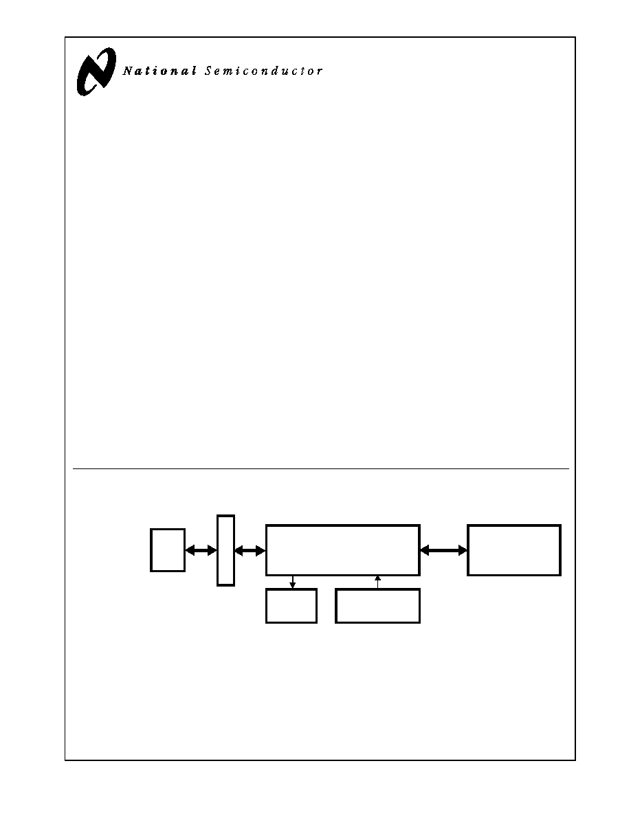
1.0 Pin Descriptions
The DP83861 pins are classified into the following interface
categories (each is described in the sections that follow):
-- MAC Interface
-- TP Interface
-- JTAG Interface
-- E
2
PROM Interface
-- Clock Interface
-- LED Interface
-- Device Configuration / Strapping Options
-- Reset
-- Power and Ground Pins
-- Special Connect Pins
Note: Strapping pin option
(BOLD) (e.g. AN_EN)
Type: I
Inputs
Type: O
Output
Type: O_Z
Tristate Output
Type: I/O_Z
Tristate Input_Output
Type: S
Strapping Pin
Type: PU
Pull-up
Type: PD
Pull-down
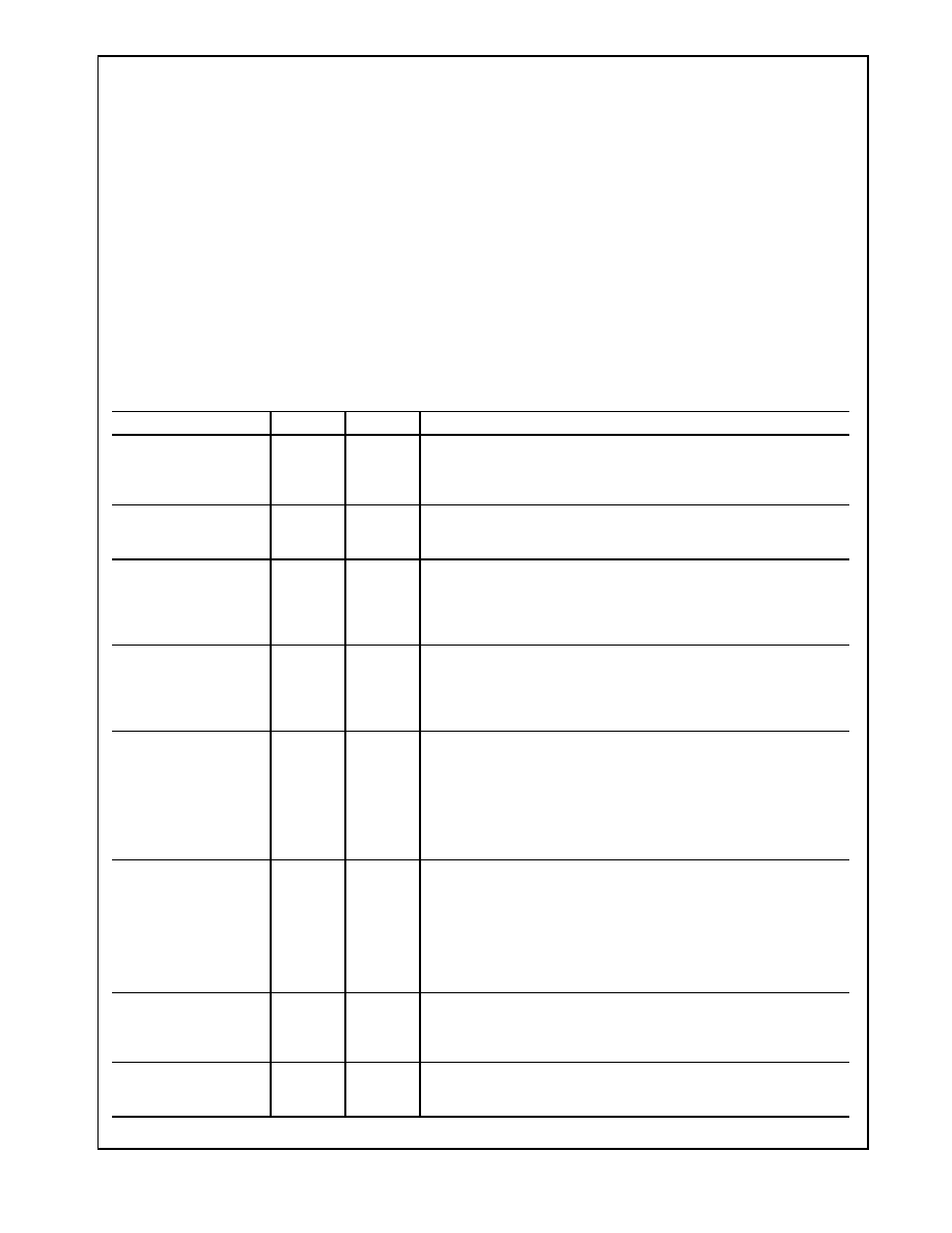
1.1 MAC Interface
Signal Name
Type
Pin #
Description
MDC
I
151
MANAGEMENT DATA CLOCK: Synchronous clock to the MDIO
management data input/output serial interface which may be asyn-
chronous to transmit and receive clocks. The maximum clock rate is
2.5 MHz with no minimum clock rate.
MDIO
I/O
150
MANAGEMENT DATA I/O: Bi-directional management instruc-
tion/data signal that may be sourced by the station management en-
tity or the PHY. This pin requires a 1.5 k
pullup resistor.
CRS
O
111
CARRIER SENSE: Asserted high to indicate the presence of carrier
due to receive or transmit activity in Half Duplex mode. This signal is
not defined (LOW) for 1000BASE-T Full Duplex mode. For
1000BASE-T, 100BASE-TX and 10BASE-T Full Duplex operation
CRS is asserted only for receive activity.
COL
O
110
COLLISION DETECT: Asserted high to indicate detection of a colli-
sion condition (assertion of CRS due to simultaneous transmit and re-
ceive activity) in Half Duplex modes. This signal is not synchronous
to either MII clock (GTX_CLK, TX_CLK or RX_CLK). This signal is not
defined (LOW) for Full Duplex modes.
TX_CLK
O
130
TRANSMIT CLOCK (10 Mb/s and 100 Mb/s): Continuous clock sig-
nal generated from REF_CLK and driven by the PHY during 10Mb/s
and 100 Mb/s operation. It is used on the MII to clock all MII Transmit
(data, error) signals into the PHY.
The Transmit Clock frequency is constant and the frequency is
2.5 MHz for 10Mb/s mode and 25 MHz for 100Mb/s mode.
TX_CLK should not be confused with the TX_TCLK signal.
TXD0
TXD1
TXD2
TXD3
TXD4
TXD5
TXD6
TXD7
I
146
145
144
141
140
139
138
135
TRANSMIT DATA: These signals carry 4B data nibbles (TXD[3:0])
during 10 Mb/s and 100 Mb/s MII mode and 8-bit data (TXD[7:0]) in
1000 Mb/s GMII mode. They are synchronous to the Transmit Clocks
(TX_CLK, GTX_CLK. Transmit data is input enabled by TX_EN for all
modes all sourced by the controller.
TX_EN
I
134
TRANSMIT ENABLE: Active high input driven by the MAC request-
ing transmission of the data present on the TXD lines (nibble data for
10 Mb/s and 100 Mb/s mode and 8-bit data for 1000 Mb/s GMII
mode.)
GTX_CLK
I
147
GMII-TRANSMIT CLOCK: This continuous clock signal is sourced
from the upper level MAC to the PHY. Nominal frequency of 125 MHz,
derived in the MAC from its 125 MHz reference clock.