 | –≠–ª–µ–∫—Ç—Ä–æ–Ω–Ω—ã–π –∫–æ–º–ø–æ–Ω–µ–Ω—Ç: DP83901A | –°–∫–∞—á–∞—Ç—å:  PDF PDF  ZIP ZIP |

TL F 10469
DP83901A
SNIC
Serial
Network
Interface
Controller
November 1995
DP83901A SNIC
Serial Network Interface Controller
General Description
The DP83901A Serial Network Interface Controller (SNIC) is
a microCMOS VLSI device designed for easy implementa-
tion of CSMA CD local area networks These include Ether-
net (10BASE5) Thin Ethernet (10BASE2) and Twisted-pair
Ethernet (10BASE-T) The overall SNIC solution provides
the Media Access Control (MAC) and Encode-Decode
(ENDEC) functions in accordance with the IEEE 802 3 stan-
dard
The integrated ENDEC module allows Manchester encod-
ing and decoding via a differential transceiver and phase
lock loop at 10 Mbit sec Also included is a collision detect
translator and diagnostic loopback capability
(Continued)
Features
Y
Compatible with IEEE 802 3
10BASE5
10BASE2
10BASE-T
Y
Dual 16-byte DMA channels
Y
16-byte internal FIFO
Y
Network statistics storage
Y
Supports physical multicast and broadcast address
filtering
Y
10 Mbit sec Manchester encoding and decoding plus
clock recovery
Y
No external precision components required
Y
Efficient buffer management implementation
Y
Transmitter can be selected for half or full step mode
Y
Integrated squelch on receive and collision pairs
Y
3 levels of loopback supported
Y
Utilizes independent system and network clocks
Y
Lock Time 5 bits typical
Y
Decodes Manchester data with up to
g
18 ns jitter
1 0 System Diagram
TL F 10469 ≠ 1
TRI-STATE
is a registered trademark of National Semiconductor Corporation
C1995 National Semiconductor Corporation
RRD-B30M115 Printed in U S A
General Description
(Continued)
The MAC function (NIC) provides simple and efficient pack-
et transmission and reception control by means of unique
dual DMA channels and an internal FIFO Bus arbitration
and memory control logic are integrated to reduce board
cost and area overheads
SNIC used in conjunction with the DP8392 Coaxial Trans-
ceiver Interface (CTI) provides a comprehensive 2 chip solu-
tion for IEEE 802 3 networks and is designed for easy inter-
face to the latest 10BASE-T transceivers
Due to the inherent constraints of CMOS processing isola-
tion is required at the differential signal interfaces for
10BASE5 and 10BASE2 applications Capacitive or induc-
tive isolation may be used
Table Of Contents
1 0 SYSTEM DIAGRAM
2 0 PIN DESCRIPTION
3 0 BLOCK DIAGRAM
4 0 FUNCTIONAL DESCRIPTION
5 0 TRANSMIT RECEIVE PACKET
ENCAPSULATION DECAPSULATION
6 0 DIRECT MEMORY ACCESS CONTROL (DMA)
7 0 PACKET RECEPTION
8 0 PACKET TRANSMISSION
9 0 REMOTE DMA
10 0 INTERNAL REGISTERS
11 0 INITIALIZATION PROCEDURE
12 0 LOOPBACK DIAGNOSTICS
13 0 BUS ARBITRATION
14 0 PRELIMINARY ELECTRICAL CHARACTERISTICS
15 0 SWITCHING CHARACTERISTICS
16 0 AC TIMING TEST CONDITIONS
17 0 PHYSICAL DIMENSIONS
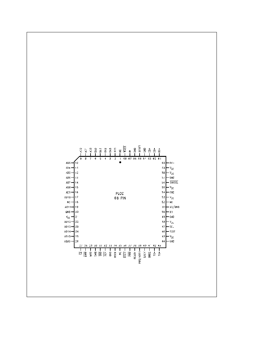
Connection Diagram
TL F 10469 ≠ 2
Top View
Order Number DP83901AV
See NS Package Number V68A
2

Pin Description
Pin No
Pin Name
I O
Description
BUS INTERFACE PINS
2
PRD
O
PORT READ
Enables data from external latch on to local bus during a memory write cycle to
local memory (remote write operation) This allows asynchronous transfer of data from the
system memory to local memory
3 ≠ 6
RA0 ≠ RA3
I
REGISTER ADDRESS
These four pins are used to select a register to be read or written The
state of these inputs is ignored when the NIC is not in slave mode (CS high)
7 ≠ 17
AD0 ≠ AD15
I O Z
MULTIPLEXED ADDRESS DATA BUS
19
Register Access with DMA inactive CS low and ACK returned from SNIC pins AD0≠AD7 are
22 ≠ 25
used to read and write register data AD8≠AD15 float during I O transfers SRD SWR pins are
used to select direction of transfer
Bus Master with BACK input asserted
During t1 of memory cycle AD0 ≠ AD15 contain address
During t2 t3 t4 AD0 ≠ AD15 contain data (word transfer mode)
During t2 t3 t4 AD0 ≠ AD7 contain data AD8 ≠ AD15 contain address (byte transfer mode)
Direction of transfer is indicated by SNIC on MWR MRD lines
26
ADS0
I O Z
ADDRESS STROBE 0
Input with DMA inactive and CS low latches RA0≠RA3 inputs on falling edge If high data
present on RA0≠RA3 will flow through latch
Output When Bus Master latches address bits (A0≠A15) to external memory during DMA
transfers
27
CS
O
CHIP SELECT
Chip Select places controller in slave mode for mP access to internal registers
Must be valid through data portion of bus cycle RA0 ≠ RA3 are used to select the internal
register SWR and SRD select direction of data transfer
28
MWR
O Z
MASTER WRITE STROBE
(Strobe for DMA transfers)
Active low during write cycles (t2 t3 tw) to buffer memory Rising edge coincides with the
presence of valid output data TRI-STATE until BACK asserted
29
MRD
O Z
MASTER READ STROBE
(Strobe for DMA transfers)
Active during read cycles (t2 t3 tw) to buffer memory Input data must be valid on rising edge of
MRD TRI-STATE until BACK asserted
30
SWR
I
SLAVE WRITE STROBE
Strobe from CPU to write an internal register selected by RA0 ≠ RA3
Data is latched into the SNIC on the rising edge of this input
31
SRD
I
SLAVE READ STROBE
Strobe from CPU to read an internal register selected by RA0 ≠ RA3
The register data is output when SRD goes low
32
ACK
O
ACKNOWLEDGE
Active low when SNIC grants access to CPU Used to insert WAIT states to
CPU until SNIC is synchronized for a register read or write operation
34
BSCK
I
BUS CLOCK
This clock is used to establish the period of the DMA memory cycle Four clock
cycles (t1 t2 t3 t4) are used per DMA cycle DMA transfers can be extended by one BSCK
increments using the READY input
36
RACK
I
READ ACKNOWLEDGE
Indicates that the system DMA or host CPU has read the data placed
in the external latch by the SNIC The SNIC will begin a read cycle to update the latch
37
PWR
O
PORT WRITE
Strobe used to latch data from the SNIC into external latch for transfer to host
memory during Remote Read transfers The rising edge of PWR coincides with the presence of
valid data on the local bus
38
READY
I
READY
This pin is set high to insert wait states during a DMA transfer The SNIC will sample this
signal at t3 during DMA transfers
3

Pin Description
(Continued)
Pin No
Pin Name
I O
Description
BUS INTERFACE PINS
(Continued)
39
PRQ ADS1
O Z
PORT REQUEST ADDRESS STROBE 1
32-BIT MODE If LAS is set in the Data Configuration Register this line is programmed
as ADS1 It is used to strobe addresses A16 ≠ A31 into external latches (A16 ≠ A31 are the
fixed addresses stored in RSAR0 RSAR1) ADS1 will remain at TRI-STATE until BACK is
received
16-BIT MODE If LAS is not set in the Data Configuration Register this line is programmed as
PRQ and is used for Remote DMA Transfers The SNIC initiates a single remote DMA read or
write operation by asserting this pin In this mode PRQ will be a standard logic output
Note
This line will power up as TRI-STATE until the Data Configuration Register is programmed
40
BACK
I
BUS ACKNOWLEDGE
Bus Acknowledge is an active high signal indicating that the CPU has
granted the bus to the SNIC If immediate bus access is desired BREQ should be tied to BACK
Tying BACK to V
CC
will result in a deadlock
41
BREQ
O
BUS REQUEST
Bus Request is an active high signal used to request the bus for DMA transfers
This signal is automatically generated when the FIFO needs servicing
65
RESET
I
RESET
Reset is active low and places the SNIC in a reset immediately no packets are
transmitted or received by the SNIC until STA bit is set Affects Command Register Interrupt
Mask Register Data Configuration Register and Transmit Configuration Register The SNIC will
execute reset within 10 BSCK cycles and TXC cycles
67
INT
O
INTERRUPT
Indicates that the SNIC requires CPU attention after reception transmission or
completion of DMA transfers The interrupt is cleared by writing to the ISR (Interrupt Service
Register) All interrupts are maskable
68
WACK
I
WRITE ACKNOWLEDGE
Issued from system to SNIC to indicate that data has been written to
the external latch The SNIC will begin a write cycle to place the data in local memory
NETWORK INTERFACE PINS
42
TX
b
O
TRANSMIT OUTPUT
Differential driver which sends the encoded data to the transceiver The
outputs are source followers which require 270X pulldown resistors
43
TX
a
46
TEST
I
FACTORY TEST INPUT
Used to check the chip's internal functions Tied low during normal
operation
47
SEL
I
MODE SELECT
When high Transmit
a
and Transmit
b
are the same voltage in the idle state
When low Transmit
a
is positive with respect to Transmit
b
in the idle state at the transformer's
primary
50
X1
I
EXTERNAL OSCILLATOR INPUT
51
GND X2
O
GROUND X2
This in should normally be connected to ground It is possible to use a crystal
oscillator using X1 and GND X2 if certain precautions are taken Contact National
Semiconductor for more information
56
SNISEL
I
FACTORY TEST INPUT
For normal operation tied to V
CC
When low enables the ENDEC
module to be tested independently of the SNIC module
60
RX
b
I
RECEIVE INPUT
Differential receive input pair from the transceiver
61
RX
a
62
CD
b
I
COLLISION INPUT
Differential collision pair input from the transceiver
63
CD
a
4

Pin Description
(Continued)
Pin No
Pin Name
I O
Description
POWER SUPPLY PINS
21 48
V
CC
DIGITAL POSITIVE 5V SUPPLY PINS
53 55
20 33 49
GND
DIGITAL NEGATIVE (GROUND) SUPPLY PINS
It is suggested that a decoupling capacitor be
connected between the V
CC
and GND pins
54 66
59
V
CC
AUI RECEIVE 5V SUPPLY
Power pin supplies 5V to the AUI receiver
64
GND
AUI RECEIVE GROUND
Ground pin for AUI receiver
45
V
CC
AUI TRANSMIT 5V SUPPLY
Power pin supplies 5V to the AUI transmitter
44
GND
AUI TRANSMIT GROUND
Ground pin for AUI transmitter
58
V
CC
VCO 5V SUPPLY
Care should be taken to reduce noise on this pin as it supplies 5V to the
ENDEC's Phase Lock Loop
57
GND
VCO GROUND PIN
Care should be taken to reduce noise on this pin as it is the ground to the
ENDEC's Phase Lock Loop
NO CONNECTION
1 18
NC
NO CONNECTION
Do not connect to these pins
35 52
3 0 Block Diagram
TL F 10469 ≠ 3
FIGURE 1
5