TL F 12597
DP83936AVUL-202533
MHz
Full
Duplex
SONIC-T
Systems-Oriented
Network
Interface
Controller
with
Twisted
Pair
Interface
January 1996
DP83936AVUL-20 25 33 MHz Full Duplex SONIC
TM
-T
Systems-Oriented Network Interface Controller
with Twisted Pair Interface
General Description
The SONIC-T (Systems-Oriented Network Interface Control-
ler with Twisted Pair) is a second-generation Ethernet Con-
troller designed to meet the demands of today's high-speed
32- and 16-bit systems Its system interface operates with a
high speed DMA that typically consumes less than 5% of
the bus bandwidth Selectable bus modes provide both big
and little endian byte ordering and a clean interface to stan-
dard microprocessors The linked-list buffer management
system of SONIC-T offers maximum flexibility in a variety of
environments from PC-oriented adapters to high-speed
motherboard designs The SONIC-T can be configured for
full duplex operation Furthermore the SONIC-T integrates
a fully-compatible IEEE 802 3 Encoder Decoder (ENDEC)
and a Twisted Pair Interface which provide a one-chip solu-
tion for Ethernet when using 10BASE-T
When using
10BASE2 or 10BASE5 the SONIC-T may be paired with the
DP8392 Coaxial Transceiver Interface to achieve a simple
2-chip solution
For increased performance the SONIC-T implements a
unique buffer management scheme to efficiently process
receive and transmit packets in system memory No inter-
mediate packet copy is necessary The receive buffer man-
agement uses three areas in memory for (1) allocating addi-
tional resources (2) indicating status information and (3)
buffering packet data During reception the SONIC-T stores
packets in the buffer area then indicates receive status and
control information in the descriptor area The system allo-
cates more memory resources to the SONIC-T by adding
descriptors to the memory resource area The transmit buff-
er management uses two areas in memory
1 indicating status and control information
2 fetching packet data
The system can create a transmit queue allowing multiple
packets to be transmitted from a single transmit command
The packet data can reside on any arbitrary byte boundary
and can exist in several non-contiguous locations
Features
Y
32-bit non-multiplexed address and data bus
Y
Configurable for Full Duplex operation
Y
Auto AUI TPI selection
Y
High-speed interruptible DMA
Y
Linked-list buffer management maximizes flexibility
Y
Two independent 32-byte transmit and receive FIFOs
Y
Bus compatibility for all standard microprocessors
Y
Supports big and little endian formats
Y
Integrated IEEE 802 3 ENDEC
Y
Integrated Twisted Pair Interface
Y
Complete address filtering for up to 16 physical and or
multicast addresses
Y
32-bit general-purpose timer
Y
Loopback diagnostics
Y
Fabricated in low-power CMOS
Y
160 PQFP package
Y
Full network management facilities support the 802 3
layer management standard
Y
Integrated support for bridge and repeater applications
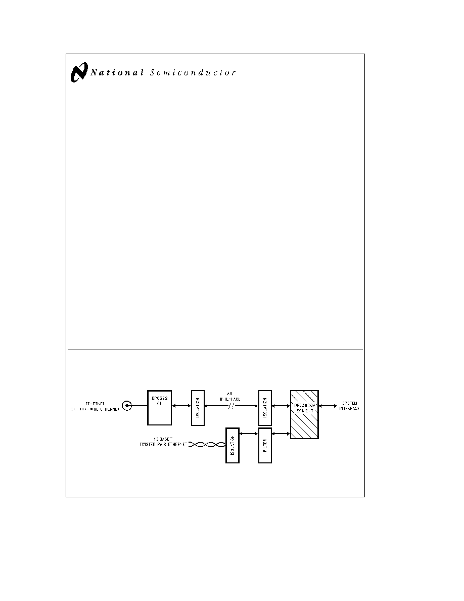
System Diagram
IEEE 802 3 Ethernet Thin-Ethernet 10BaseT Station
TL F 12597 � 1
TRI-STATE
is a registered trademark of National Semiconductor Corporation
SONIC
TM
is a trademark of National Semiconductor Corporation
C1996 National Semiconductor Corporation
RRD-B30M36 Printed in U S A
http
www national com

Table of Contents
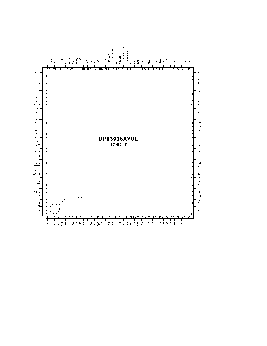
1 0 CONNECTION DIAGRAMS
1 1 Pin Connection Diagram National Intel Mode
1 2 Pin Connection Diagram Motorola Mode
2 0 PIN DESCRIPTION
3 0 FUNCTIONAL DESCRIPTION
3 1 Twisted Pair Interface Module
3 2 IEEE 802 3 Encoder Decoder (ENDEC) Unit
3 2 1 ENDEC Operation
3 2 2 Selecting an External ENDEC
3 3 Media Access Control (MAC) Unit
3 3 1 MAC Receive Section
3 3 2 MAC Transmit Section
3 3 3 Full Duplex Operation
3 4 Data Width and Byte Ordering
3 5 FIFO and Control Logic
3 5 1 Receive FIFO
3 5 2 Transmit FIFO
3 6 Status and Configuration Registers
3 7 Bus Interface
3 8 Loopback and Diagnostics
3 8 1 Loopback Procedure
3 9 Network Management Functions
4 0 TRANSMIT RECEIVE IEEE 802 3 FRAME FORMAT
4 1 Preamble and Start of Frame Delimiter (SFD)
4 2 Destination Address
4 3 Source Address
4 4 Length Type Field
4 5 Data Field
4 6 FCS Field
4 7 MAC (Media Access Control) Conformance
5 0 BUFFER MANAGEMENT
5 1 Buffer Management Overview
5 2 Descriptor Areas
5 2 1 Naming Convention for Descriptors
5 2 2 Abbreviations
5 2 3 Buffer Management Base Addresses
5 3 Descriptor Data Alignment
5 4 Receive Buffer Management
5 4 1 Receive Resource Area (RRA)
5 4 2 Receive Buffer Area (RBA)
5 4 3 Receive Descriptor Area (RDA)
5 4 4 Receive Buffer Management Initialization
5 4 5 Beginning of Reception
5 4 6 End of Packet Processing
5 4 7 Overflow Conditions
5 5 Transmit Buffer Management
5 5 1 Transmit Descriptor Area (TDA)
5 5 2 Transmit Buffer Area (TBA)
5 5 3 Preparing to Transmit
5 5 4 Dynamically Adding TDA Descriptors
6 0 SONIC-T REGISTERS
6 1 The CAM Unit
6 1 1 The Load CAM Command
6 2 Full Duplex Operation
6 3 Status Control Registers
6 4 Register Description
6 4 1 Command Register
6 4 2 Data Configuration Register
6 4 3 Receive Control Register
6 4 4 Transmit Control Register
6 4 5 Interrupt Mask Register
6 4 6 Interrupt Status Register
6 4 7 Data Configuration Register 2
6 4 8 Transmit Registers
6 4 9 Receive Registers
6 4 10 CAM Registers
6 4 11 Tally Counters
6 4 12 General Purpose Timer
6 4 13 Silicon Revision Register
7 0 BUS INTERFACE
7 1 Pin Configurations
7 2 System Configuration
7 3 Bus Operations
7 3 1 Acquiring the Bus
7 3 2 Block Transfers
7 3 3 Bus Status
7 3 4 Bus Mode Compatibility
7 3 5 Master Mode Bus Cycles
7 3 6 Bus Exceptions (Bus Retry)
7 3 7 Slave Mode Bus Cycle
7 3 8 On-Chip Memory Arbiter
7 3 9 Chip Reset
8 0 NETWORK INTERFACING
8 1 Manchester Encoder and Differential Driver
8 1 1 Manchester Decoder
8 1 2 Collision Translator
8 1 3 Oscillator Inputs
8 1 4 Power Supply Considerations
8 2 Twisted Pair Interface Module
9 0 AC AND DC SPECIFICATIONS
10 0 AC TIMING TEST CONDITIONS
http
www national com
2

1 0 Connection Diagrams
1 1 PIN CONNECTION DIAGRAM NATIONAL INTEL MODE
TL F 12597 � 2
http
www national com
3
1 0 Connection Diagrams
(Continued)
1 2 PIN CONNECTION DIAGRAM MOTOROLA MODE
TL F 12597 � 3
http
www national com
4
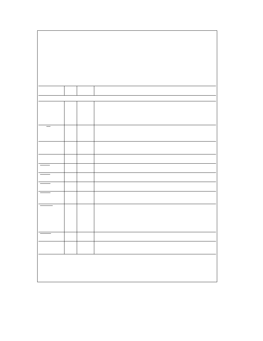
2 0 Pin Description
I
e
Input
O
e
Output
Z
e
TRI-STATE
Input TTL compatible
ECL
e
Emitter Coupled Logic type drivers for interfacing to
the Attachment Unit Interface
TP
e
Totem Pole type drivers These drivers are driven
either high or low and are always driven Drive lev-
els are CMOS compatible
TRI
e
TRI-STATE drivers These pins are driven high low
or TRI-STATE Drive levels are CMOS compatible
These pins may also be inputs (depending on the
pin)
OC
e
Open Collector type drivers
These drivers are
TRI-STATE when inactive and are driven low when
active These pins may also be inputs (depending
on the pin)
TPI
e
Twisted Pair Interface
Pin names which contain a `` '' indicate dual function pins
TABLE 2-1 Pin Description
Symbol
Driver
Direction
Description
Type
NETWORK INTERFACE PINS
EXT
I
EXTERNAL ENDEC SELECT
Tying this pin to V
CC
(EXT
e
1) disables the internal
ENDEC and allows an external ENDEC to be used Tying this pin to ground (EXT
e
0)
enables the internal ENDEC This pin must be tied either to V
CC
or ground Note the
alternate pin definitions for CRSo CRSi COLo COLi RXDo RXDi RXCo RXCi and
TXCo TXCi When EXT
e
0 the first pin definition is used and when EXT
e
1 the second
pin definition is used
AUI TP
I
ATTACHMENT UNIT INTERFACE (AUI) TWISTED PAIR (TP) SELECT
Tying this pin
to V
CC
(AUI TP
e
1) enables the AUI mode for interface with the ENDEC unit Tying this
pin to GND (AUI TP
e
0) enables the TPI Module mode for interface with the ENDEC
unit
TXOd
a
TXO
a
TPI
O
TWISTED PAIR TRANSMIT OUTPUTS
These high drive CMOS level outputs are
resistively combined external to the chip to produce a differential output signal with
TXO
b
TXOd
b
equalization to compensate for Intersymbol Interference (ISI) on the twisted pair medium
RXI
a
RXI
b
TPI
I
TWISTED PAIR RECEIVE INPUTS
These inputs feed a differential amplifier which
passes valid data to the ENDEC module
TXLED
TP
O
TRANSMIT
An active low output It is asserted for approximately 50 ms whenever the
SONIC-T Controller transmits data in either AUI or TPI modes
RXLED
TP
O
RECEIVE
An active low output It is asserted for approximately 50 ms whenever receive
data is detected in either AUI or TPI mode
COLED
TP
O
COLLISION
An active low output It is asserted for approximately 50 ms whenever the
SONIC-T Controller detects a collision in either AUI or TPI modes
POLED
TP
O
POLARITY
An active low output This signal is normally inactive When the TPI module
detects seven consecutive link pulses or three consecutive received packets with
reversed polarity it is asserted
LINKLED
TP
O
GOOD LINK
An active low output This pin operates as an output to display link integrity
status if this function has not been disabled by the LNKDIS pin described below This
output is off if the SONIC-T Controller is in AUI mode or if link testing is enabled and the
link integrity is bad (i e the twisted pair link has been broken)
This output is on if the SONIC-T Controller is in Twisted Pair Interface (TPI) mode link
integrity checking is enabled and the link integrity is good (i e the twisted pair link has
not been broken) or if the link testing is disabled
LNKDIS
I
LINK DISABLE
When this pin is tied to GND (LNKDIS
e
0) the link test pulse
generation and integrity checking function are both disabled
LOWSQL
I
LOW SQUELCH SELECT
Tying this pin to V
CC
(LOWSQL
e
1) sets the squelch mode
to use a squelch threshold level lower than that of the 10BASE-T specification (see
Section 3 1)
http
www national com
5