TL F 12499
DP83952
Repeater
Interface
Controller
with
Security
Features
(RIC
II)
PRELIMINARY
September 1995
DP83952
Repeater Interface Controller with
Security Features (RIC
TM
II)
General Description
The DP83952 RIC II Repeater Interface Controller is an
``Enhanced'' version of the DP83950 RIC RIC II is fully
backward pin and functional compatible with the RIC The
DP83952 RIC II has the same basic architecture as the RIC
with additional feature enhancements RIC II provides addi-
tional network security options additional statistics for re-
peater activities and a faster processor interface When
RIC II is used in a ``non-secure'' mode it functions in the
same manner as the DP83950 RIC When RIC II is used in a
``secure'' mode it restricts unauthorized nodes from intrud-
ing and or eavesdropping into the network The RIC II uti-
lizes internal CAMs to store compare addresses of valid
nodes when network security is desired
RIC II implements the IEEE 802 3 multiport repeater unit
specifications It is fully compliant with the 802 3 repeater
specification for the repeater segment partition and jabber
lockup protection state machines (Continued)
Features
Y
Compliant with the IEEE 802 3 Repeater Specification
Y
13 network connections (ports) per chip
Y
Selectable on-chip twisted-pair transceivers
Y
Cascadable for large hub applications
Y
Compatible with AUI compliant transceivers
Y
On-chip Elasticity Buffer Manchester encoder and
decoder
Y
Separate Partition state machines for each port
Y
Compatible with 802 3k Hub Management requirements
Y
Provides port status information for LED displays in-
cluding receive collision partition link status and jab-
ber
Y
Power-up configuration options
Repeater and Partition Specifications Transceiver Inter-
face Status Display Processor Operations
Y
Simple processor interface for repeater management
and port disable
Y
On-chip Event Counters and Event Flag Arrays
Y
Serial Management Bus Interface to combine packet
and repeater status information
Y
CMOS process for low power dissipation
Y
Single 5V supply
Security Features
Y
Power-up configuration options
Y
Prevents unauthorized eavesdropping and or intrusion
on a per port basis
Y
58 on-chip CAMs (Content Addressable Memory) allow
storage of acceptable addresses
Y
Learn mode automatically records addresses of at-
tached nodes
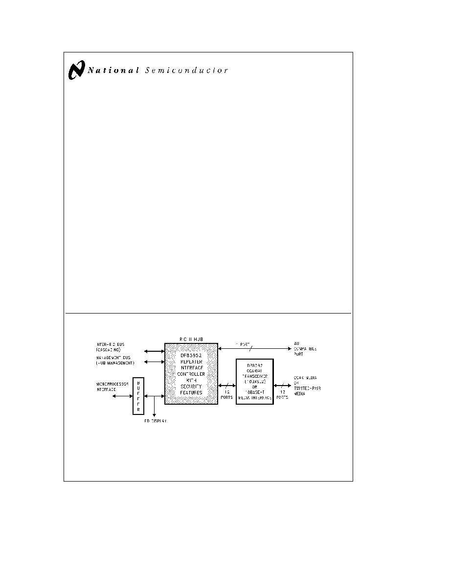
1 0 System Diagram
TL F 12499 � 1
TRI-STATE is a registered trademark of National Semiconductor Corporation
RIC
TM
Inter-RIC
TM
and SONIC
TM
are trademarks of National Semiconductor Corporation
PAL
is a registered trademark of and used under license from Advanced Micro Devices Inc
GAL
is a registered trademark of Lattice Semiconductor
C1995 National Semiconductor Corporation
RRD-B30M115 Printed in U S A

General Description
(Continued)
The RIC II repeater design consists of two major functional
blocks Segment Specific Block and Shared Functional
Blocks The Segment Specific Block implements the IEEE
repeater requirements on a per network port basis while the
Shared Functional Blocks implement the core logic blocks
for the IEEE repeater unit The Shared Functional Blocks
consist of repeater receive multiplexor an on chip phase
lock loop (PLL) decoder for Manchester data an Elasticity
Buffer for preamble regeneration transmit encoder and de-
multiplexor for Manchester data
The DP83952 RIC II can be connected up to 13 cable seg-
ments via its network interface ports One port is fully AUI
compatible and is able to connect to an external MAU using
the maximum length of AUI cable The other 12 ports have
integrated 10BASE-T transceivers These transceiver func-
tions may be bypassed so that the RIC II may be used with
external transceivers such as the DP8392 coaxial trans-
ceivers
A large repeater unit can be constructed by cascading
RIC IIs together via the Inter-RIC
TM
bus All the cascaded
RIC IIs form a single repeater unit
The RIC II is configurable for specific applications It pro-
vides port status information for LED array displays and a
simple interface for system processors The RIC II possess-
es multi-function counters and status flag arrays to facilitate
network statistics gathering A serial Hub Management In-
terface is available for the collection of data in Managed
Hub applications
Table Of Contents
1 0 SYSTEM DIAGRAM
2 0 CONNECTION DIAGRAMS
3 0 PIN DESCRIPTION
4 0 BLOCK DIAGRAM
5 0 FUNCTIONAL DESCRIPTION
5 1 Summary of DP83952 RIC II Feature Enhancements
from DP83950B RIC
5 2 Overview of RIC II Functions
5 3 Description of Repeater Operations
5 4 Examples of Packet Repetition Scenarios
5 5 Description of Hardware Connection for Inter-RIC Bus
5 6 Processor and Display Interface
5 7 Description of Hardware Connection for Processor
and Display Interface
6 0 HUB MANAGEMENT SUPPORT
6 1 Event Counting Function
6 2 Event Record Function
6 3 Management Interface Operation
6 4 Description of Hardware Connection for Management
Interface
7 0 PORT BLOCK FUNCTIONS
7 1 Transceiver Functions
7 2 Segment Partition
7 3 Port Status Register Functions
7 4 Local Ports and Inter-RIC Bus Expected Activity
7 5 Local Ports and Inter-RIC Bus Data Field Contents
8 0 RIC II REGISTERS
9 0 AC AND DC SPECIFICATIONS
10 0 TIMING AND LOAD DIAGRAMS
11 0 AC TIMING TEST CONDITIONS
2