D
P
8395
3 (R
IC
2A
)
R
e
pe
ater
In
ter
f
ace
C
o
n
t
r
o
ller
wit
h S
ecu
r
i
ty F
eatu
r
e
s
, In
ter
n
a
l
D
r
iv
er
s
and
Int
e
gr
at
ed F
ilte
r
s
�
1998 National Semiconductor Corporation
www.national.com
PRELIMINARY
March 1998
DP83953 (RIC2A)
Repeater Interface Controller with Security Features,
Internal Drivers and Integrated Filters
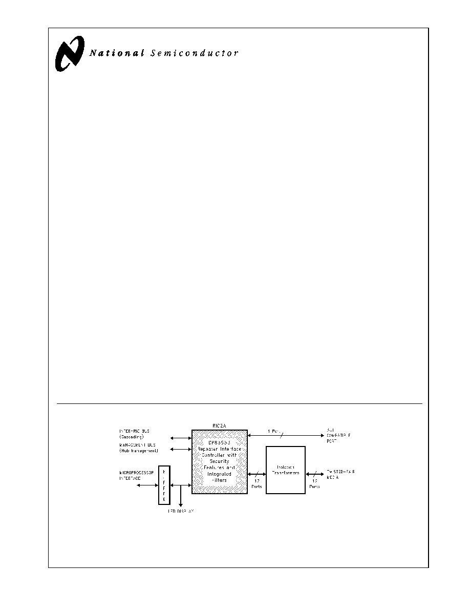
General Description
The DP83953 Repeater Interface Controller with Security
Features and Integrated Transmit Filters (RIC2A) is an en-
hanced version of the DP83952 Repeater Interface Control-
ler with Security Features (RIC II). The RIC2A integrates
driver and filter circuitry into the RIC II design.
The functionality of the RIC2A is essentially similar to the
RIC II, but the pin definitions have been modified to reflect
the added integrated drivers and filters. Additionally, the
power and ground pin locations have been rearranged.
Therefore, the RIC2A is not a drop in replacement for the
RIC ll.
The RIC2A is National Semiconductor's managed repeater
solution designed to comply with IEEE 802.3 Repeater
Specifications. Segment partition and jabber lockup protec-
tion state machines are implemented in accordance with
this standard. The RIC2A has thirteen network interface
ports available, including an AUI compatible port. The AUI
port incorporates drivers to connect an external MAU using
maximum length cable. Similarly, the other twelve interface
ports integrate 10BASE-T transceivers with supporting driv-
er and transmit filter circuitry. (continued)
Features
T
Fully compliant with the IEEE 802.3 Repeater Specifica-
tion
T
12 IEEE 802.3 10BASE-T compatible ports with built-in
drivers and analog transmit filters; additional external
isolation transformers are required to implement hubs
FAST
�
and TRI-STATE
�
are registered trademarks of National Semiconductor Corporation.
100RIC
TM
is a trademark of National Semiconductor Corporation
SONIC
TM
is a trademark of National Semiconductor Corporation
Ethernet is a trademark of Xerox Corporation
GAL
�
is a registered trademark of Lattice Semiconductor
PAL
�
is a registered trademark of and license from Advanced Micro Devices, Inc.
T
1 IEEE 802.3 compatible AUI port
T
Cascadable for larger hub applications
T
On chip Elasticity Buffer, Manchester encoder and de-
coder
T
Separate Partition state machines for each port
T
Compatible with 802.3k Hub Management require-
ments
T
LED displays to provide port status information, includ-
ing receive, collision, partition, jabber and link status,
T
Power-up configuration options
T
Repeater and Partition Specifications, Status Display,
Processor Operations
T
Simple processor interface for repeater management
and port disable.
T
On-chip Event Counters and Event Flag Arrays
T
Serial Management Bus Interface to combine packet
and repeater status information
T
Single 5V supply
The Security Features
T
Prevents unauthorized eavesdropping and/or intrusion
on a per port basis
T
58 On Chip CAMs (Content Addressable Memory) al-
low storage of acceptable addresses
T
Learn mode automatically records addresses of at-
tached node
System Diagram

2
www.national.com
General Description
(continued)
The RIC2A repeater consists of two major functional
blocks: The segment specific block and the shared func-
tional blocks. The segment specific block incorporates rele-
vant IEEE specifications on a per port basis. The shared
functional blocks incorporate core logic for the entire IEEE
repeater unit. The core logic blocks consist of a repeater
receive multiplexor, a phase locked loop (PLL), a Manches-
ter decoder, an elasticity buffer, a transmit encoder and a
demultiplexor.
A larger repeater system may be constructed by cascading
several RIC2A devices via the Inter-RIC bus. This method
of cascading allows the RIC2A system to function as a sin-
gle repeater unit without introducing additional repeater
hops.
The RIC2A is configurable for specific applications. It pro-
vides port status information for LED array displays and a
simple interface for system processors. The RIC2A pos-
sesses multifunctional counters and status flag arrays to
facilitate network statistics gathering, as well as a serial
Hub Management Interface Bus for collecting, event data in
managed hub applications.
Table of Contents
1.0
Connection Diagram . . . . . . . . . . . . . . . . . . . . . . . . . . . 3
2.0
Pin Descriptions . . . . . . . . . . . . . . . . . . . . . . . . . . . . . . . 5
3.0
Block Diagrams . . . . . . . . . . . . . . . . . . . . . . . . . . . . . . 10
4.0
Functional Description . . . . . . . . . . . . . . . . . . . . . . . . . 12
4.1
Summary of DP83953 RIC2A Feature
Enhancements from DP83952 RIC II . . . . . . . . . 12
4.2
Overview Of RIC2A Functions . . . . . . . . . . . . . . . 12
4.3
Description Of Repeater Operations . . . . . . . . . . 14
4.4
Examples Of Packet Repetition
Scenarios . . . . . . . . . . . . . . . . . . . . . . . . . . . . . . . 19
4.5
Description Of Hardware Connection For Inter-ric
Bus . . . . . . . . . . . . . . . . . . . . . . . . . . . . . . . . . . . . 27
4.6
Processor and Display Interface . . . . . . . . . . . . . 28
4.7
Description Of Hardware Connection For Processor
And Display Interface . . . . . . . . . . . . . . . . . . . . . . 30
5.0
HUB Management Support . . . . . . . . . . . . . . . . . . . . . 35
5.1
Event Counting Function . . . . . . . . . . . . . . . . . . 35
5.2
Event Record Function . . . . . . . . . . . . . . . . . . . . 36
5.3
Management Interface Operation . . . . . . . . . . . . 37
5.4
Description of Hardware Connection for
Management Interface . . . . . . . . . . . . . . . . . . . . 43
6.0
Port Block Functions . . . . . . . . . . . . . . . . . . . . . . . . . 44
6.1
Transceiver Functions . . . . . . . . . . . . . . . . . . . . 44
6.2
Segment Partition . . . . . . . . . . . . . . . . . . . . . . . . 47
6.3
Port Status Register Functions . . . . . . . . . . . . . . 47
6.4
Local Ports and Expected Activity . . . . . . . . . . . 49
7.0
RIC2A Registers . . . . . . . . . . . . . . . . . . . . . . . . . . . . . 50
8.0
Board Layout Recommendations . . . . . . . . . . . . . . . 75
9.0
DC and AC Specification . . . . . . . . . . . . . . . . . . . . . . 77
10.0
Physical Dimensions . . . . . . . . . . . . . . . . . . . . . . . . . 90

3
www.national.com
1.0 Connection Diagram
Order Number DP83953VUL
NS Package Number VUL160A
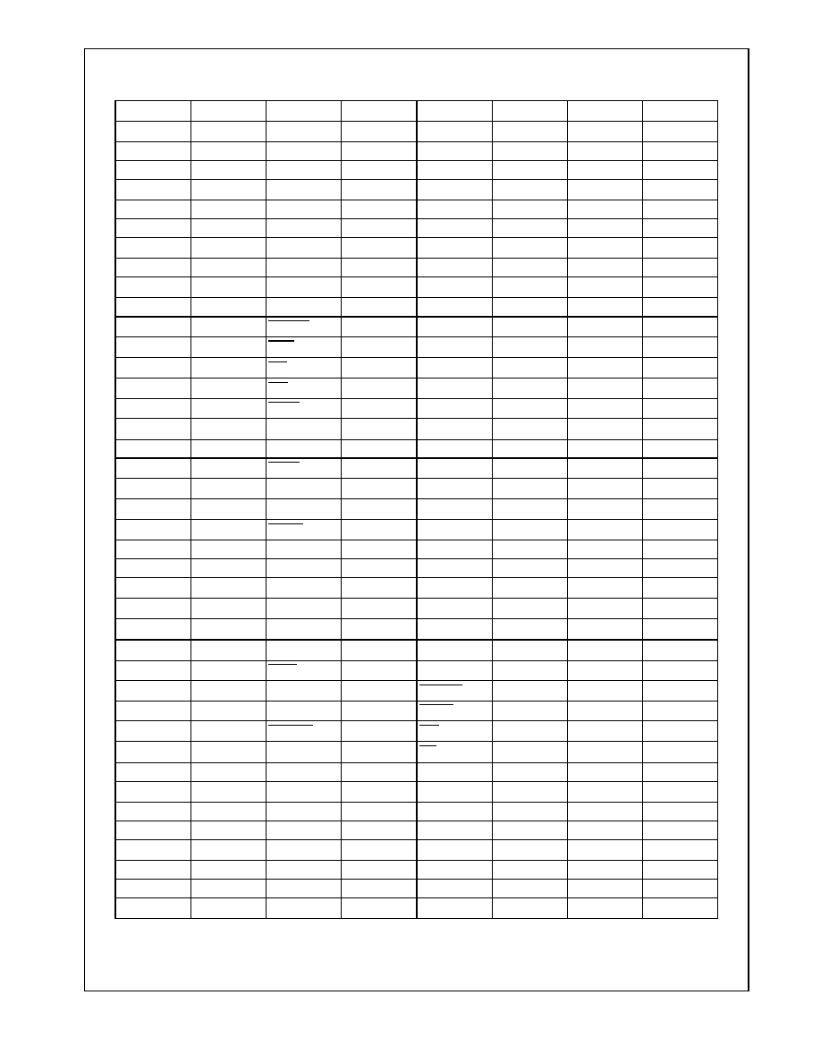
1.0 Connection Diagram
(Continued)
4
www.national.com
Note 1: NC = No Connect
Note 2: Port
V
DD
and GND are denoted as
V
DD
Px and GNDPx, where x=2-13 for all twisted pair ports.
Note 3: The path to each port
V
DD
and GND must have a very low impedance.
12 T.P. Ports + 1 AUI
PIN NAME
PIN NO.
PIN NAME
PIN NO.
PIN NAME
PIN NO.
PIN NAME
PIN NO.
GNDP13
40
V
DD
80
TXO2-
120
GND
160
TXO13-
39
GND
79
TXO2+
119
TEST_11
159
TXO13+
38
IRC
78
GNDP2
118
TEST_10
158
TXO12-
37
IRE
77
V
DD
P2
117
TEST_9
157
TXO12+
36
IRD
76
RXI2-
116
TEST_8
156
GNDP12
35
COLN
75
RXI2+
115
TEST_7
155
V
DD
P12
34
V
DD
74
RX1-
114
NC
154
RXI12-
33
GND
73
RX1+
113
FILTTL
153
RXI12+
32
PKEN
72
CD1-
112
V
DD
WS
152
RXI11-
31
RXMPLL
71
CD1+
111
GNDWS
151
RXI11+
30
BUFEN
70
TX1-
110
RXI7-
150
V
DD
P11
29
RDY
69
TX1+
109
RXI7+
149
GNDP11
28
ELI
68
V
DD
AUI
108
V
DD
P7
148
TXO11-
27
RTI
67
GND AUI
107
GNDP7
147
TXO11+
26
STR0
66
NC
106
TXO7-
146
TXO10-
25
V
DD
65
NC
105
TXO7+
145
TXO10+
24
GND
64
NC
104
TXO6-
144
GNDP10
23
STR0
63
NC
103
TXO6+
143
V
DD
P10
22
ACTND
62
V
DD
102
GNDP6
142
RXI10-
21
ANYXND
61
GND
101
V
DD
P6
141
RXI10+
20
ACKO
60
CLKIN
100
RXI6-
140
RXI9-
19
MRXC
59
RA4
99
RXI6+
139
RXI9+
18
MEN
58
RA3
98
RXI5-
138
V
DD
P9
17
MRXD
57
RA2
97
RXI5+
137
GNDP9
16
MCRS
56
RA1
96
V
DD
P5
136
TXO9-
15
V
DD
55
RA0
95
GNDP5
135
TXO9+
14
GND
54
V
DD
PLL
94
TXO5-
134
TXO8-
13
ACKI
53
GNDPLL
93
TXO5+
133
TXO8+
12
ACTNS
52
MLOAD
92
TXO4-
132
GNDP8
11
ANYXNS
51
CDEC
91
TXO4+
131
V
DD
P8
10
PCOMP
50
WR
90
GNDP4
130
RXI8-
9
NC
49
RD
89
V
DD
P4
129
RXI8+
8
TEST_6
48
D7
88
RXI4-
128
V
DD
A
7
TEST_5
47
D6
87
RXI4+
127
GNDA
6
TEST_4
46
D5
86
RXI3-
126
RTX
5
TEST_3
45
D4
85
RXI3+
125
REQ
4
TEST_2
44
D3
84
V
DD
P3
124
NC
3
RXI13-
43
D2
83
GNDP3
123
TEST_1
2
RXI13+
42
D1
82
TXO3-
122
V
DD
1
V
DD
P13
41
D0
81
TXO3+
121

5
www.national.com
2.0 Pin Descriptions
TP = Twisted Pair interface compatible, TT = TTL compatible, I = Input, O = Output, Analog = current dependent effect,
AL = AUI Level, AD = AUI Drive
Pin Name
Pin No.
Driver
Type
I/O
Description
Network Interface Pins
RXI2- to RXI13-
TP
I
Twisted Pair Receive Input Negative
RXI2+ to RXI13+
TP
I
Twisted Pair Receive Input Positive
TXO2- to TXO13-
TP
O
Twisted Pair Transmit Output Negative
TXO2+ to TXO13+
TP
O
Twisted Pair Transmit Output Positive
FILTTL
153
TT
I
FILter/TTL: This pin can be utilized for the PCB diagnostic pur-
poses.
0: Normal repeater operation
1: Differential transmit signals change to TTL level +TX and de-
layed +TX.
REQ
4
Analog
I
Equalization Resistor: A resistor connected between this pin and
GND or
V
DD
adjusts the equalization step amplitude on the
Manchester encoded transmit data. Care must be taken to ensure
system timing integrity when using cable lengths greater than
100m. The value here is dependent upon board layout.
RTX
5
Analog
I
Extended Cable Resistor: A resistor connected between this pin
and GND or
V
DD
adjusts the amplitude of the differential transmit
outputs. Care must be taken to ensure system timing integrity
when using cable lengths greater than 100m. The value here is
dependent upon board layout.
AUI Port
CD1+
111
AL
I
AUI Collision Detect Input Positive
CD1-
112
AL
I
AUI Collision Detect Input Negative
RX1+
113
AL
I
AUI Receive Input Positive
RX1-
114
AL
I
AUI Receive Input Negative
TX1+
109
AD
O
AUI Transmit Output Positive
TX1-
110
AD
O
AUI Transmit Output Negative