
TL F 11718
DP8440-40DP8440-25DP8441-40DP8441-25
microCMOS
Programmable
1664
Mbit
Dynamic
RAM
ControllerDriver
February 1995
DP8440-40 DP8440-25 DP8441-40 DP8441-25
microCMOS Programmable 16 64 Mbit
Dynamic RAM Controller Driver
General Description
The DP8440 41 Dynamic RAM Controllers provide an easy
interface between dynamic RAM arrays and 8- 16- 32- and
64-bit microprocessors The DP8440 41 DRAM Controllers
generate all necessary control and timing signals to suc-
cessfully interface and design dynamic memory systems
With significant enhancements over the DP8420 21 22
predecessors the DP8440 41 are suitable for high perform-
ance memory systems These controllers support page and
burst accesses for fast page static column and nibble
DRAMs Refreshes and accesses are arbitrated on chip
RAS low time during refresh and RAS precharge time are
guaranteed by these controllers Separate precharge coun-
ters for each RAS output avoid delayed back to back ac-
cesses due to precharge when using memory interleaving
Programmable features make the DP8440 41 DRAM Con-
trollers flexible enough to fit many memory systems
Features
Y
40 MHz and 25 MHz operation
Y
Page detection
Y
Automatic CPU burst accesses
Y
Support 1 4 16 64 Mbits DRAMs
Y
High capacitance drivers for RAS CAS WE and Q out-
puts
Y
Support for fast page static column and nibble mode
DRAMs
Y
High precision PLL based delay line
Y
Byte enable for word size up to 32 bits on the DP8440
or 64 bits on the DP8441
Y
Automatic Internal Refresh
Y
Staggered RAS-Only refresh
Y
Burst and CAS-before-RAS refresh
Y
Error scrubbing during refresh
Y
TRI-STATE
outputs
Y
Easy interface to all major microprocessors
Block Diagram
TL F 11718 ≠ 1
FIGURE 1
TRI-STATE
is a registered trademark of National Semiconductor Corporation
C1995 National Semiconductor Corporation
RRD-B30M75 Printed in U S A
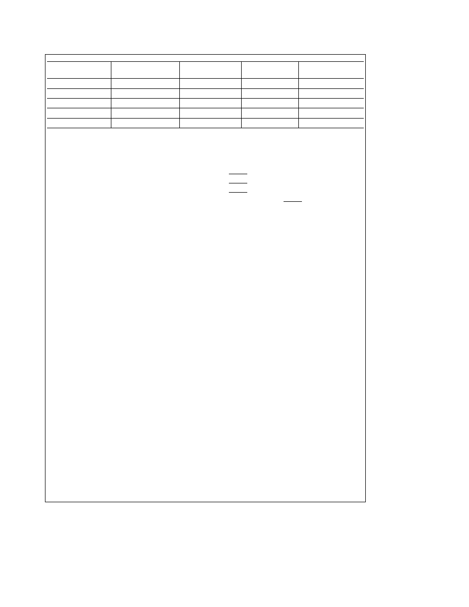
DRAM
Maximum Clock
Package
Bus Width
Largest DRAM
Controller
Frequency
Type
Supporting
Possible
DP8440V-40
40 MHz
84-Pin PLCC
8 16 32
16 Mbits
DP8440VLJ-40
40 MHz
100-Pin PQFP
8 16 32
16 Mbits
DP8440VLJ-25
25 MHz
100-Pin PQFP
8 16 32
16 Mbits
DP8441VLJ-40
40 MHz
100-Pin PQFP
8 16 32 64
64 Mbits
DP8441VLJ-25
25 MHz
100-Pin PQFP
8 16 32 64
64 Mbits
Table of Contents
1 0 CONNECTION DIAGRAMS
2 0 FUNCTIONAL INTRODUCTION
3 0 SIGNAL DESCRIPTION
3 1 Address and Control Signals
3 2 DRAM Control Signals
3 3 Refresh Signals
3 4 Reset and Programming Signals
3 5 Clock Inputs
3 6 Power Signals and Capacitor Input
4 0 PROGRAMMING AND RESETTING
4 1 Reset
4 2 Programming Sequence
4 3 Programming Selection Bits
5 0 ACCESS MODES
5 1 Opening Access
5 2 Normal Mode
5 3 Page Mode
5 4 Burst Access
5 5 Inner Page Burst Access
6 0 REFRESH MODES
6 1 Auto-Internal Refresh
6 2 Externally Controlled Refresh
6 3 Error Scrubbing during Refresh
6 4 Extending Refresh
6 5 Refresh Types
7 0 WAIT SUPPORT
7 1 DTACK During Opening Access
7 2 DTACK During Page Access
7 3 DTACK During Burst Access
7 4 Next Address or Early DTACK Support
8 0 ABSOLUTE MAXIMUM RATINGS
9 0 DC ELECTRICAL CHARACTERISTICS
10 0 LOAD CAPACITANCE
11 0 AC TIMING PARAMETERS
12 0 AC TIMING WAVEFORMS
CLK and DECLK Timing
Refresh Timing
Refresh and Access Timing
Programming and Initialization Period Timing
Normal Mode Access Timing
Page Mode Access Timing
Burst Mode Access Timing
13 0 ERRATA
14 0 PHYSICAL DIMENSIONS
2
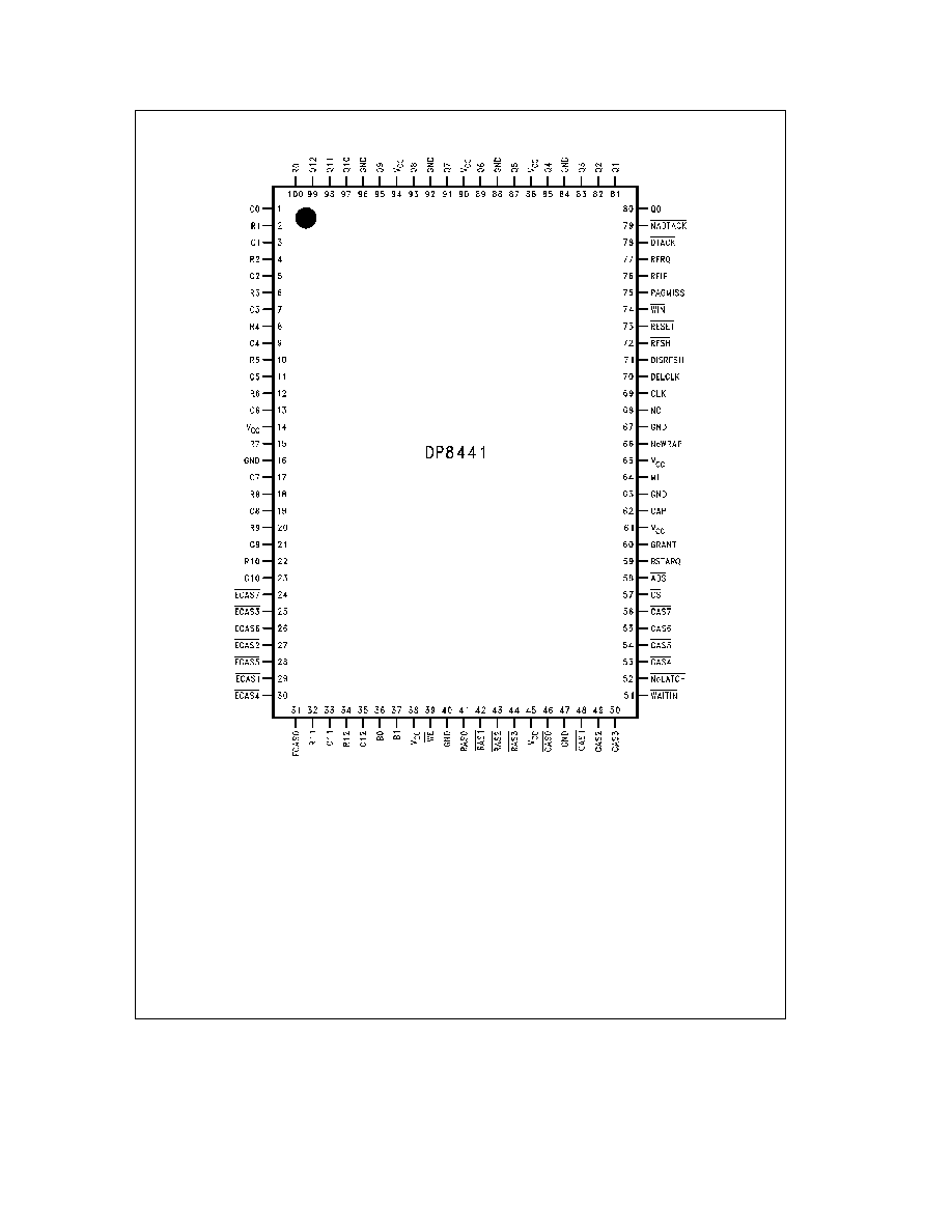
1 0 Connection Diagrams
TL F 11718 ≠ 2
Top View
FIGURE 2
Order Number DP8441VLJ-40 (40 MHz Operation) DP8441VLJ-25 (25 MHz Operation)
See NS Package Number VLJ100A
3
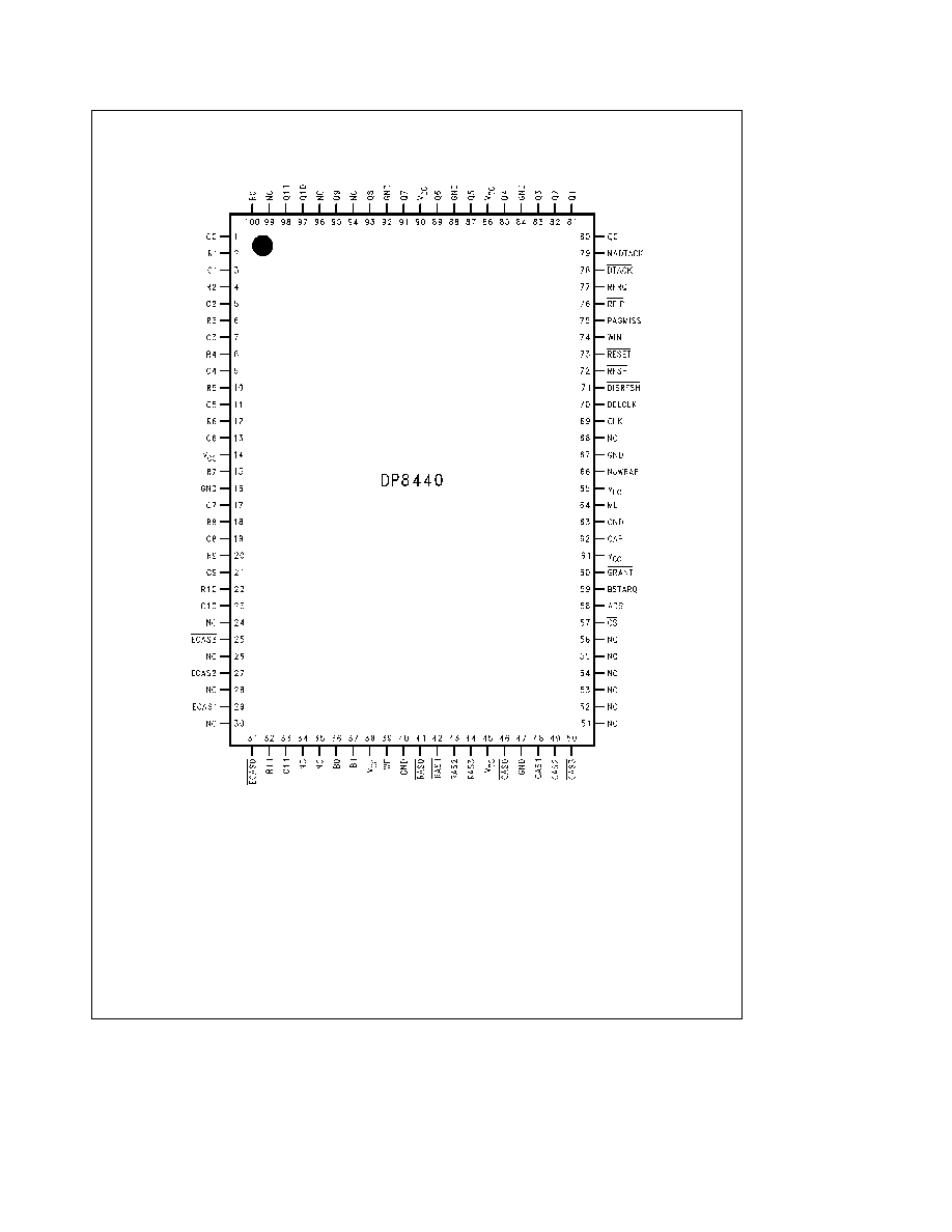
1 0 Connection Diagrams
(Continued)
TL F 11718 ≠ 38
Top View
FIGURE 3
Order Number DP8440VLJ-40 (40 MHz Operation) DP8440VLJ-25 (25 MHz Operation)
See NS Package Number VLJ100A
4
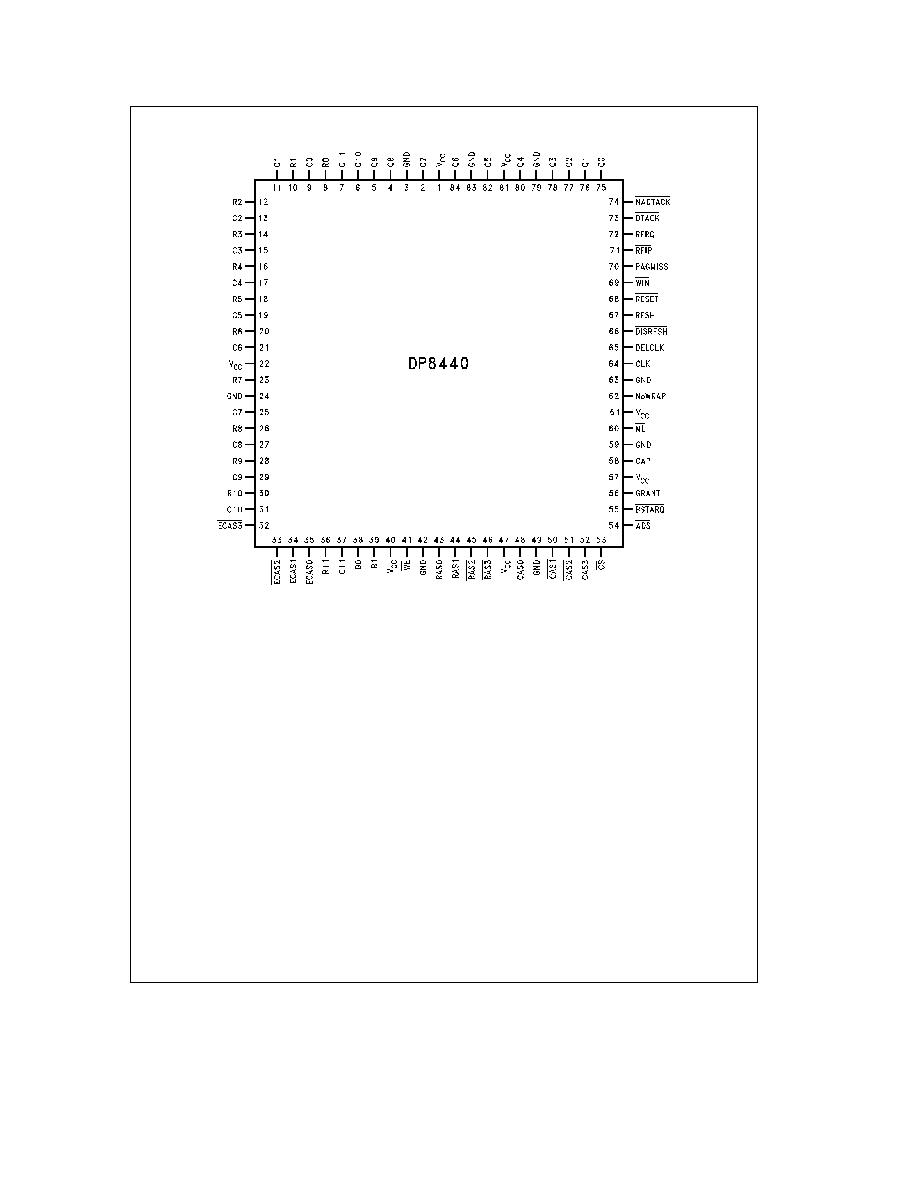
1 0 Connection Diagrams
(Continued)
TL F 11718 ≠ 3
Top View
FIGURE 4
Order Number DP8440V-40 (40 MHz Operation)
See NS Package Number V84A
5