DP8459 All-Code Data Synchronizer
General Description
The DP8459 Data Synchronizer is an integrated phase
locked loop circuit which has been designed for application
in magnetic hard disk, flexible (floppy) disk, optical disk, and
tape drive memory systems for data re-synchronization and
clock recovery with any standard recording code, operating
to 25 Mb/s. The DP8459 is provided in a 28-pin PCC
package. Zero phase start is employed during both data and
reference clock lock sequences for rapid acquisition. An
optional
(Customer-controlled)
synchronization
field
frequency-acquisition feature guarantees lock, accommo-
dating the preamble types used with GCR (Group Code
Recording), MFM (Modified Frequency Modulation), the
[1,N] run length limited (RLL) codes, and either of the
standard 2,7 RLL codes. Precise synchronization window
generation is achieved via an internal, self-aligning delay line
which remains accurate independent of temperature, power
supply, external component and IC process variations. The
DP8459 also incorporates a digitally controlled ( MICROW-
IRE
TM
bus compatible) strobe function with 5-bit resolution
which allows for margin testing, error recovery routines, and
precise window calibration. The PLL filter resides external to
the chip, with two ports provided to allow significant design
flexibility. Synchronization pattern detection circuitry issues a
PREAMBLE DETECTED signal when a pre-determined
length of the user-selected pattern is encountered. All digital
input and output signals are TTL compatible and a single,
+5V power supply is required. The DP8459V is offered as a
DP8459V-10
(250
Kbit/sec
thru
10
Mbits/sec)
or
DP8459V-25 (250 Kbits/sec thru 25 Mbit/sec), see AC
Electrical Characteristics.
Features
n
Fully integrated dual-gain PLL
n
Zero phase start lock sequence
n
250 Kbit/sec�25 Mbit/sec data rate range
n
Frequency lock capability (optional) for all standard
recording codes
n
Digital window strobe control, 5-bit resolution
n
Two-port PLL filter network
n
PLL free-run (Coast) control for optical disk defects
n
Synchronization pattern (preamble lock) detection
n
Non-glitching multiplexed read/write clock output
n
+5V supply
n
DP8459 supplied in 28-pin plastic chip carrier (PCC)
and 40-pin TapePak packages
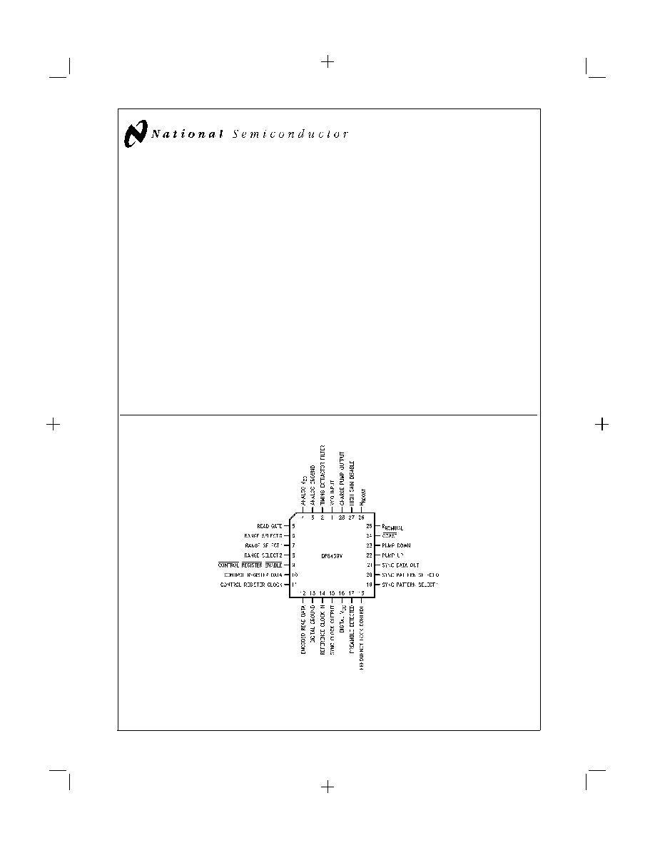
Connection Diagrams
FIGURE 1. DP8459 in 28-Pin Plastic Chip Carrier (PCC) V-Type Package Order Number DP8459V-10 or DP8459V-25
TapePak
�
is a registered trademark of National Semiconductor Corporation.
MICROWIRE
TM
is a trademark of National Semiconductor Corporation.
TL/F/9322-6
ADVANCED
December 1995
DP8459
All-Code
Data
Synchronizer
DP8459
� 1996 National Semiconductor Corporation
TL/F/9322
http:\\www.national.com
1
PrintDate=1996/07/31 PrintTime=11:05:38 ds009322 Rev. No. 1
Proof
1

Connection Diagrams
TapePak
�
TL/F/9322-39
Top ViewOrder Number DP8459TP-10 or DP8459TP-25See NS Package TP40A
PrintDate=1996/07/31 PrintTime=11:05:39 ds009322 Rev. No. 1
Proof
2
2
http:\\www.national.com
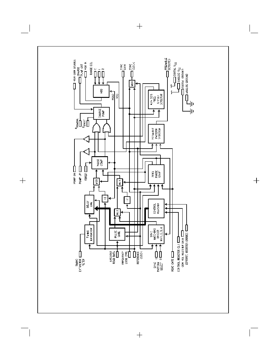
System Diagram
FIGURE 2. DP8459 System Block Diagram
TL/F/9322-8
http:\\www.national.com
3
PrintDate=1996/07/31 PrintTime=11:05:39 ds009322 Rev. No. 1
Proof
3

1.0 Pin Descriptions
DP8459 28-pin PCC package
Pin #
POWER SUPPLY
16
DIGITAL V
CC
: 5.0V
�
5%. (Note 1 )
4
ANALOG V
CC
: 5.0V
�
5%. (Note 1 )
13
DIGITAL GROUND.
3
ANALOG GROUND.
TTL LEVEL LOGIC INPUTS
5
READ GATE (RG): Read mode control input, active high (logical-one). Assertion causes the PLL to lock to
the ENCODED READ DATA, employing a zero phase start routine. Deassertion causes the PLL to lock the
REFERENCE CLOCK input, also employing a zero phase start routine. READ GATE timing is allowed to
be fully asynchronous.
6, 7, 8
RANGE SELECT 0, 1, 2 (RS0, RS1, RS2): Control the operating frequency range of the VCO. A 2:1
continuously variable sub-range is available within each of 6 allowed selections, enabling the VCO to
operate at any frequency within a 96:1 range from 500 kHz to 50 MHz.
9
CONTROL REGISTER ENABLE (CRE): A logical Low level allows the CONTROL REGISTER CLOCK to
clock data into the Control Register via the CONTROL REGISTER DATA input; a logical HIGH level
latches the register data and issues the information to the appropriate circuitry.
10
CONTROL REGISTER DATA (CRD): Control Register data input.
11
CONTROL REGISTER CLOCK (CRC): Negative edge triggered Control Register clock input.
12
ENCODED READ DATA (ERD): Incoming TTL-level data derived from the storage media; issued from a
pulse detector circuit. Each positive edge represents a single recorded code bit.
14
REFERENCE CLOCK (RFC): A reference frequency input required for DP8459 operation. The RFC
frequency must be accurate and highly stable (crystal or servo derived) and equivalent to the 2F frequency
for the MFM or [2,7] codes (i.e., equal to, but not derived from the VCO frequency).
18
FREQUENCY LOCK CONTROL (FLC): Selects or de-selects the frequency lock function during a READ
operation. Has no effect with READ GATE deasserted; frequency lock is automatically employed for the full
duration of time READ GATE is deasserted regardless of the level of the FLC input. With READ GATE
high and FLC low (logical-zero) the PLL is forced to lock to the pattern frequency selected via the SYNC
PATTERN SELECT inputs. When high (logical-one) frequency lock action is terminated and the PLL
employs a pulse gate to accommodate random disk data patterns. FLC may be tied to PREAMBLE
DETECTED output pin for self-regulated frequency lock control. FLC timing is allowed to be fully
asynchronous.
20, 19
SYNC PATTERN SELECT 0, 1 (SP0, SP1): Control inputs for selection of the preamble type being
employed. These inputs determine the pattern to which the PLL will frequency-lock during preamble
acquisition (if frequency lock is employed) and for which the PREAMBLE DETECTED circuitry searches.
24
COAST (CST): Control for Coast function. The Coast function may be activated when READ GATE is
either high or low. When the COAST input is low (logical-zero), the phase comparator is disabled and held
in a cleared state, allowing the VCO to coast regardless of ENCODED READ DATA input activity (READ
GATE high) or REFERENCE CLOCK input activity (READ GATE low). No other circuit functions are
disturbed. When high (logical-one), the phase comparator operates normally.
27
HIGH-GAIN DISABLE (HGD): Charge Pump gain switch control. When low (logical-zero), the charge pump
input current is the combined value of the currents at both R
BOOST
and R
NOMINAL
pins. When high
(logical-one), charge pump input current is taken from the R
NOMINAL
pin only. HGD may be tied either to
READ GATE or PREAMBLE DETECTED for self-regulated gain control.
TTL LEVEL LOGIC OUTPUTS
15
SYNCHRONIZED CLOCK (SCK): Issues the VCO signal following READ GATE assertion and completion
of zero phase start sequence; issues REFERENCE CLOCK input signal when READ GATE is deasserted.
Multiplexer switching is achieved without glitches.
17
PREAMBLE DETECTED (PDT): Issues a high level (logical-one) following assertion of READ GATE,
completion of the zero phase start sequence, and the detection of approximately 32 sequential pulses of
1T, 2T or 3T period preamble, or 16 sequential pulses of 4T period preamble, depending on state of SYNC
PATTERN SELECT inputs (T = VCO period). Following preamble detection, the output remains latched
high until de-assertion of READ GATE. The PDT output will be at a logical zero state whenever READ
GATE is inactive.
PrintDate=1996/07/31 PrintTime=11:05:40 ds009322 Rev. No. 1
Proof
4
4
http:\\www.national.com
1.0 Pin Descriptions
(Continued)
Pin #
TTL LEVEL LOGIC OUTPUTS
21
SYNCHRONIZED DATA (SD): A reconstructed replica of the ENCODED READ DATA signal,
time-stabilized and synchronized to the SYNCHRONIZED CLOCK output.
22
PUMP UP (PU): Active HIGH whenever the phase comparator issues a pump-up signal to the charge
pump. The PU pin is an open-emitter output requiring an external passive pull down resistor whenever in
active use. The output should be allowed to float when not needed.
23
PUMP DOWN (PD): Active HIGH whenever the phase comparator issues a pump-down signal to the
charge pump. The PD pin is an open-emitter output requiring an external passive pull down resistor
whenever in active use. The output should be allowed to float when not needed.
ANALOG SIGNAL PINS
28
CHARGE PUMP OUTPUT: The output of the high-speed, switching bi-directional current source circuitry of
the charge pump. The external, passive PLL filter network is established between this pin, the VCO INPUT
pin, and ground.
1
VCO INPUT: The high-impedance control voltage input to the voltage controlled oscillator (VCO). The
external, passive PLL filter network is established between this pin, the CHARGE PUMP OUTPUT pin, and
ground.
2
TIMING EXTRACTOR FILTER: A pin for the connection of external, passive components employed to
stabilize the delay line timing extraction circuitry. Delay accuracy is not a function of external component
values or tolerances.
25
R
NOMINAL
: A resistor is tied between this pin and V
CC
to set the charge pump
nominal operating current.
The current is internally multiplied by 2 for charge pump use.
26
R
BOOST
: A resistor is tied between this pin and V
CC
to set the charge pump
boost (or adder) current. The
R
BOOST
resistor is effectively paralleled with the R
NOMINAL
resistor when the HIGH GAIN DISABLE input is
inactive (logical-zero); thus the sum of the resistor currents sets the total input current. The input current is
multiplied by 2 within the charge pump circuitry.
Note 1: These pins should always be tied together; they are not intended to be used with separate power supplies.
2.0 Circuit Operation
In the non-Read mode, the DP8459 PLL is locked to the
REFERENCE CLOCK signal. This permits the VCO to remain
at a frequency very close to the encoded data clock rate while
the PLL is "idling" and thus will minimize the frequency step
and associated lock time encountered at the initiation of lock to
ENCODED READ DATA. Frequency acquisition is employed
in the non-Read mode to ensure lock.
Note: The REFERENCE CLOCK signal is employed by circuitry which sets the
time delay of the internal delay line. This requires the REFERENCE CLOCK
signal to be present
at all times at a stable and accurate frequency for proper
DP8459 operation.
At the assertion of READ GATE, which is allowed to be done
asynchronously (no timing requirements), and following the
completion of two subsequent VCO cycles, the DP8459 VCO
is stopped momentarily and restarted in accurate phase
alignment with the second data bit which arrives following the
VCO pause. This minimization of phase misalignment
between the ENCODED READ DATA and the VCO (referred to
as zero phase start, or ZPS) significantly reduces data lock
acquisition time.
The DP8459 incorporates a preamble-specific frequency
acquisition feature which may be employed at the user's
option.
The
frequency
acquisition
feature
is
intended
specifically for use within hard or pseudo-hard sectored
systems where READ GATE is asserted only within a
preamble. With the READ GATE active (logical-one) and the
FREQUENCY LOCK CONTROL
(FLC)
input
active
(logical-zero), the DP8459 will be forced to lock to the exact
preamble frequency selected at the SYNC PATTERN SELECT
inputs. The frequency discriminating action of the PLL
provided in this mode produces a lock-in range equivalent to
the available VCO operating range and thus eliminates the
possibility of fractional-harmonic lock. Windowing (pulse gate
action; see Pulse Gate, Section 2.1) is not employed in the
frequency acquisition mode and thus quadrature lock is
prevented (see National Semiconductor Application Note
AN-414, APPS Mass Storage Handbook #1, 1986, for an
explanation of typical false lock modes). The DP8459 will
remain in the frequency acquisition mode until the FLC input is
deactivated (logical-one). In ordinary hard sectored or
pseudo-hard sectored operation, the PREAMBLE DETECTED
(PDT) output is tied to the FLC input for automatic switching
from frequency acquisition to phase lock following internal
detection of the selected preamble by the DP8459. The
Customer may choose to intervene in this path and extend the
frequency lock period. However, the DP8459
must be placed
in the phase lock mode (FLC deactivated--logical-one) prior
to encountering the end of the preamble, or loss of lock will
result.
Switching
of
the
FLC
input
may
be
done
asynchronously (no set-up or hold timing requirements).
The PREAMBLE DETECTED (PDT) output will become active
(logical-one) following READ GATE assertion, completion of
the
ZPS
sequence
and
the
subsequent
detection
of
approximately 32 ENCODED READ DATA (ERD) pulses of the
1T, 2T or 3T preamble types, or 16 ENCODED READ DATA
(ERD) pulses of the 4T preamble type (see specification
tables), and will remain active (logical-one) until deassertion of
READ GATE.
The Customer has the option of employing an elevated PLL
bandwidth during preamble acquisition (or at any other time)
for an extended capture range. An R
BOOST
pin is provided to
http:\\www.national.com
5
PrintDate=1996/07/31 PrintTime=11:05:41 ds009322 Rev. No. 1
Proof
5