 | –≠–ª–µ–∫—Ç—Ä–æ–Ω–Ω—ã–π –∫–æ–º–ø–æ–Ω–µ–Ω—Ç: DP8481N | –°–∫–∞—á–∞—Ç—å:  PDF PDF  ZIP ZIP |
TL F 5862
DP8481
TTL
to
10k
ECL
Level
Translator
with
Latch
June 1986
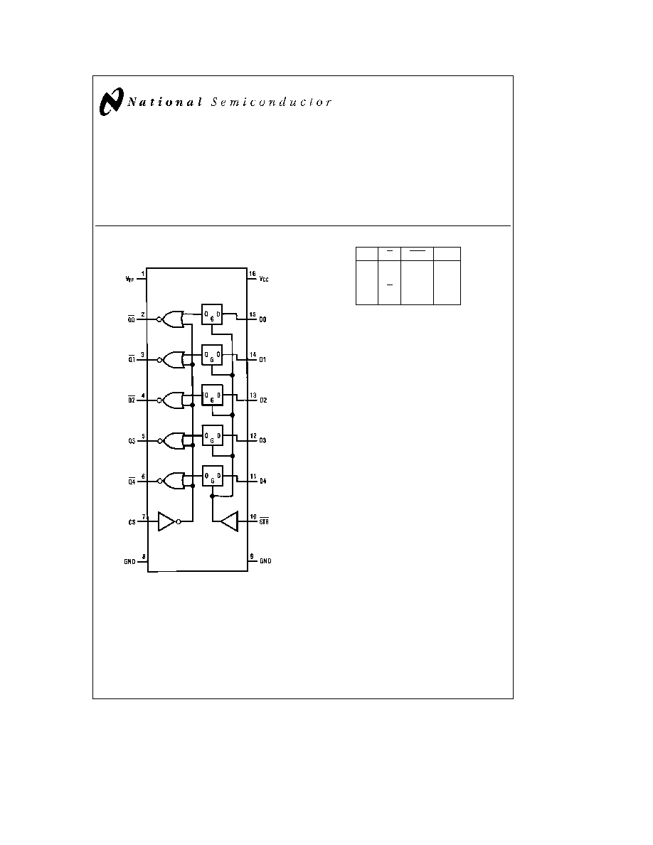
DP8481 TTL to 10k ECL Level Translator with Latch
General Description
This circuit translates TTL input levels to ECL output levels
and provides a fall-through latch The outputs are gated with
CS providing for wire ORing of outputs The strobe and chip
select inputs operate at ECL levels
Features
Y
16-pin flat-pack or DIP
Y
ECL control inputs
Y
CS provided for wire ORing of output bus
Y
10k ECL I O compatible
Y
3 0 ns typical propagation delay
Logic and Connection Diagram
Dual-In-Line Package
TL F 5862 ≠ 1
Top View
Truth Table
D
Q
STR
CS
H
L
L
H
L
H
L
H
X
Q
H
H
X
L
X
L
H
e
high level (most positive)
L
e
low level (most negative)
X
e
don't care
Order Number
DP8481F DP8481J or DP8481N
See NS Package
F16B J16A or N16A
C1995 National Semiconductor Corporation
RRD-B30M115 Printed in U S A
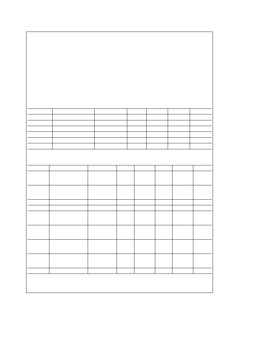
Absolute Maximum Ratings
(Note 1)
If Military Aerospace specified devices are required
please contact the National Semiconductor Sales
Office Distributors for availability and specifications
V
EE
Supply Voltage
b
8V
V
CC
Supply Voltage
7V
Input Voltage (ECL)
GND to V
EE
Input Voltage (TTL)
b
1V to 5 5V
Output Current
50 mA
Maximum Power Dissipation at 25 C
Molded Package
1476 mW
Storage Temperature
b
65 C to
a
150 C
Derate molded package 11 8 mW C above 25 C
Recommended Operating Conditions
V
EE
Supply Voltage
b
5 2V
g
10%
V
CC
Supply Voltage
5 0V
g
10%
T
A
Ambient Temperature
0 C to 75 C
Electrical Characteristics
(TTL Logic) (Notes 2 and 3)
Symbol
Parameter
Conditions
Min
Typ
Max
Units
V
IL
Input Low Voltage
0 8
V
V
IH
Input High Voltage
2 0
V
I
IL
Input Low Current
V
IN
e
0 5V
b
25
b
200
m
A
I
IH
Input High Current
V
IN
e
2 5V
1 0
40
m
A
V
CLAMP
Input Clamp Voltage
I
IN
e b
12 mA
b
0 9
b
1 2
V
I
CC
Supply Current
V
CC
e
5 5V
10
20
mA
Electrical Characteristics
(ECL Logic) (Notes 2 and 3)
Symbol
Parameter
Conditions
T
A
Min
Typ
Max
Units
V
IL
Input Low Voltage
V
EE
e b
5 2V
0 C
b
1870
b
1490
25 C
b
1850
b
1475
mV
75 C
b
1830
b
1450
V
IH
Input High Voltage
V
EE
e b
5 2V
0 C
b
1145
b
840
25 C
b
1105
b
810
mV
75 C
b
1045
b
720
I
IL
Input Low Current
V
IN
e b
1 8V
55
150
m
A
I
IH
Input High Current
V
IN
e b
0 8V
85
200
m
A
V
OL
Output Low Voltage
V
EE
e b
5 2V
0 C
b
1870
b
1665
25 C
b
1850
b
1650
mV
75 C
b
1830
b
1625
V
OH
Output High Voltage
V
EE
e b
5 2V
0 C
b
1000
b
840
25 C
b
960
b
810
mV
75 C
b
900
b
720
V
OLC
Output Low Voltage
V
EE
e b
5 2V
0 C
b
1645
25 C
b
1630
mV
75 C
b
1605
V
OHC
Output High Voltage
V
EE
e b
5 2V
0 C
b
1020
25 C
b
980
mV
75 C
b
920
I
EE
Supply Current
V
EE
e b
5 7V
b
70
b
90
mA
2
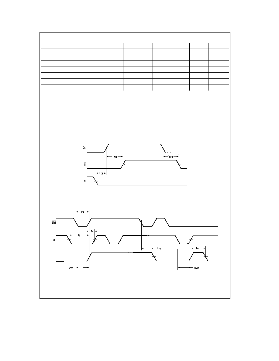
Switching Characteristics
(Notes 2 and 4)
Symbol
Parameter
Conditions
Min
Typ
Max
Units
t
PD1
Strobe To Output Delay
1 5
3 0
6 0
ns
t
PD2
Data To Output Delay
2 5
4 5
7 5
ns
t
S
Data Set-Up Time to Strobe
5 0
2 0
ns
t
H
Data Hold Time
1 0
0
ns
t
PW
Strobe Pulse Width
5 0
3 0
ns
t
PD3
Chip Select to Output Delay
1 0
2 5
4 0
ns
t
SCS
Data Set-Up Time to Chip Select
5 5
3 0
ns
Note 1
``Absolute Maximum Ratings'' are those values beyond which the safety of the device cannot be guaranteed They are not meant to imply that the device
should be operated at these limits The table of ``Electrical Characteristics'' provides conditions for actual device operation
Note 2
Unless otherwise specified min max limits apply across the 0 C to 75 C ambient temperature range in still air and across the specified supply variations
All typical values are for 25 C and nominal supply
Note 3
All currents into device pins are shown as positive all currents out of device pins are shown as negative All voltages are referenced to ground unless
otherwise specified
Note 4
Unless otherwise specified all AC measurements are referenced from the 1 5V level of the TTL input and to from the 50% point of the ECL signal and a
50X resistor to
b
2V is the load ECL input rise and fall times are 2 0 ns
g
0 2 ns from 20% to 80% TTL input characteristic is 0V to 3V with t
r
e
t
f
s
3 ns measured
from 10% to 90%
Switching Time Waveforms
TL F 5862 ≠ 2
TL F 5862 ≠ 3
3

4
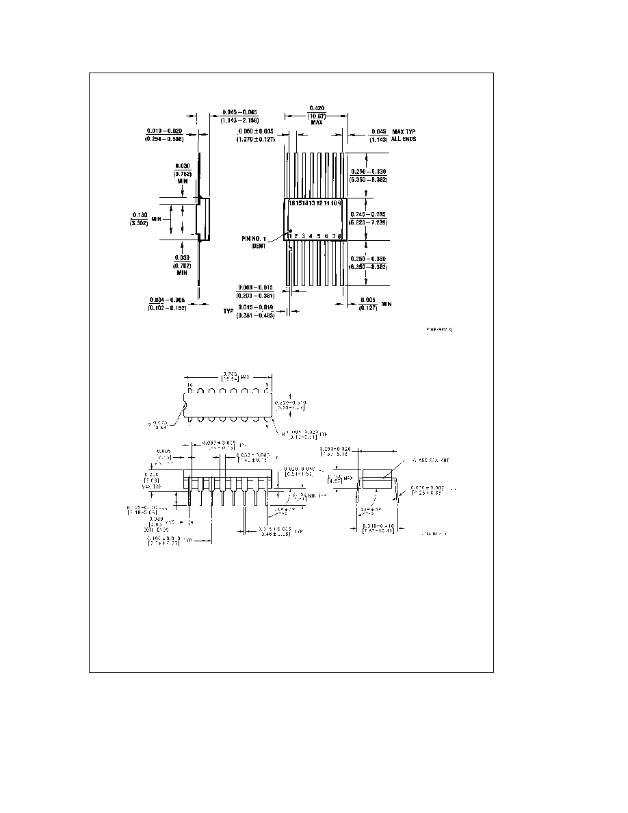
Physical Dimensions
inches (millimeters)
Ceramic Flat Package (F)
Order Number DP8481F
NS Package F16B
Ceramic Dual-In-Line Package (J)
Order Number DP8481J
NS Package J16A
5