TL F 9980
DP8572ADP8572AM
Real
Time
Clock
(RTC)
May 1993
DP8572A DP8572AM Real Time Clock (RTC)
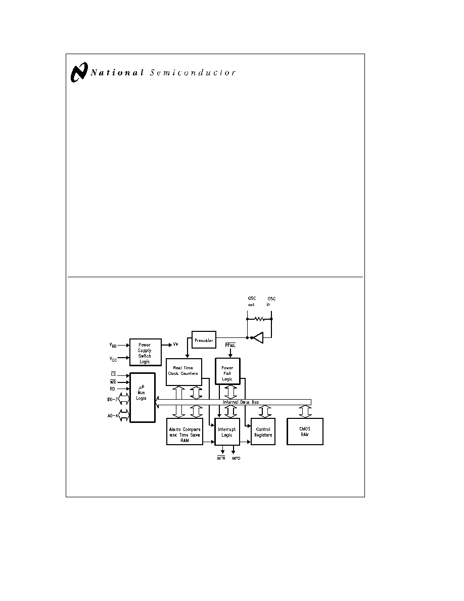
General Description
The DP8572A (8572AM
militarized version) is intended for
use in microprocessor based systems where information is
required for multi-tasking data logging or general time of
day date information This device is implemented in low
voltage silicon gate microCMOS technology to provide low
standby power in battery back-up environments The cir-
cuit's architecture is such that it looks like a contiguous
block of memory or I O ports The address space is orga-
nized as 2 software selectable pages of 32 bytes This in-
cludes the Control Registers the Clock Counters the Alarm
Compare RAM and the Time Save RAM Any of the RAM
locations that are not being used for their intended purpose
may be used as general purpose CMOS RAM
Time and date are maintained from 1 100 of a second to
year and leap year in a BCD format 12 or 24 hour modes
Day of week day of month and day of year counters are
provided Time is controlled by an on-chip crystal oscillator
requiring only the addition of the crystal and two capacitors
The choice of crystal frequency is program selectable
Power failure logic and control functions have been integrat-
ed on chip This logic is used by the RTC to issue a power
fail interrupt and lock out the mp interface The time power
fails may be logged into RAM automatically when V
BB
l
V
CC
Additionally two supply pins are provided When
V
BB
l
V
CC
internal circuitry will automatically switch from
the main supply to the battery supply Status bits are provid-
ed to indicate initial application of battery power system
power and low battery detect
(Continued)
Features
Y
Full function real time clock calendar
12 24 hour mode timekeeping
Day of week and day of years counters
Four selectable oscillator frequencies
Parallel resonant oscillator
Y
Power fail features
Internal power supply switch to external battery
Power Supply Bus glitch protection
Automatic log of time into RAM at power failure
Y
On-chip interrupt structure
Periodic alarm and power fail interrupts
Y
Up to 44 bytes of CMOS RAM
Y
MIL-STD-883C compliant
Y
SMD
5962-91641-01MJX (future)
Block Diagram
TL F 9980 ≠ 1
FIGURE 1
TRI-STATE
is a registered trademark of National Semiconductor Corporation
C1995 National Semiconductor Corporation
RRD-B30M75 Printed in U S A
8572A
Absolute Maximum Ratings
(Notes 1
2)
Specifications for the 883 version of this product are
listed separately
Supply Voltage (V
CC
)
b
0 5V to
a
7 0V
DC Input Voltage (V
IN
)
b
0 5V to V
CC
a
0 5V
DC Output Voltage (V
OUT
)
b
0 5V to V
CC
a
0 5V
Storage Temperature Range
b
65 C to
a
150 C
Power Dissipation (PD)
500 mW
Lead Temperature (Soldering 10 sec )
260 C
Operation Conditions
Min
Max
Unit
Supply Voltage (V
CC
) (Note 3)
4 5
5 5
V
Supply Voltage (V
BB
) (Note 3)
2 2 V
CC
b
0 4
V
DC Input or Output Voltage
0 0
V
CC
V
(V
IN
V
OUT
)
Operation Temperature (T
A
)
b
40
a
85
C
Electr-Static Discharge Rating TBD
1
kV
Transistor Count
10 300
Typical Values
i
JA
DIP
Board
59 C W
Socket
65 C W
i
JA
PLCC
Board
80 C W
Socket
88 C W
DC Electrical Characteristics
V
CC
e
5V
g
10% V
BB
e
3V V
PFAIL
l
V
IH
C
L
e
100 pF (unless otherwise specified)
Symbol
Parameter
Conditions
Min
Max
Units
V
IH
High Level Input Voltage
Any Inputs Except OSC IN
2 0
V
(Note 4)
OSC IN with External Clock
V
BB
b
0 1
V
V
IL
Low Level Input Voltage
All Inputs Except OSC IN
0 8
V
OSC IN with External Clock
0 1
V
V
OH
High Level Output Voltage
I
OUT
e b
20 mA
V
CC
b
0 1
V
(Excluding OSC OUT)
I
OUT
e b
4 0 mA
3 5
V
V
OL
Low Level Output Voltage
I
OUT
e
20 mA
0 1
V
(Excluding OSC OUT)
I
OUT
e
4 0 mA
0 25
V
I
IN
Input Current (Except OSC IN)
V
IN
e
V
CC
or GND
g
1 0
m
A
I
OZ
Output TRI-STATE Current
V
OUT
e
V
CC
or GND
g
5 0
m
A
I
LKG
Output High Leakage Current
V
OUT
e
V
CC
or GND
g
5 0
m
A
MFO INTR Pins
Outputs Open Drain
I
CC
Quiescent Supply Current
F
OSC
e
32 768 kHz
(Note 7)
V
IN
e
V
CC
or GND (Note 5)
250
m
A
V
IN
e
V
CC
or GND (Note 6)
1 0
mA
V
IN
e
V
IH
or V
IL
(Note 6)
12 0
mA
F
OSC
e
4 194304 MHz or
4 9152 MHz
V
IN
e
V
CC
or GND (Note 6)
8
mA
V
IN
e
V
IH
or V
IL
(Note 6)
20
mA
I
CC
Quiescent Supply Current
V
BB
e
GND
(Single Supply Mode)
V
IN
e
V
CC
or GND
(Note 7)
F
OSC
e
32 768 kHz
40
m
A
F
OSC
e
4 9152 MHz or
7 5
mA
4 194304 MHz
I
BB
Standby Mode Battery
V
CC
e
GND
Supply Current
OSC OUT
e
open circuit
(Note 7)
other pins
e
GND
F
OSC
e
32 768 kHz
10
m
A
F
OSC
e
4 9152 MHz or
400
m
A
4 194304 MHz
I
BLK
Battery Leakage
2 2V
s
V
BB
s
4 0V
other pins at GND
V
CC
e
GND V
BB
e
4 0V
1 5
m
A
V
CC
e
5 5V V
BB
e
2 2V
b
5
m
A
Note 1
Absolute Maximum Ratings are those values beyond which damage to the device may occur
Note 2
Unless otherwise specified all voltages are referenced to ground
Note 3
For F
OSC
e
4 194304 or 4 9152 MHz V
BB
minimum
e
2 8V In battery backed mode V
BB
s
V
CC
b
0 4V
Single Supply Mode Data retention voltage is 2 2V min
In single Supply Mode (Power connected to V
CC
pin) 4 5V
s
V
CC
s
5 5V
Note 4
This parameter (V
IH
) is not tested on all pins at the same time
Note 5
This specification tests I
CC
with all power fail circuitry disabled by setting D7 of Interrupt Control Register 1 to 0
Note 6
This specification tests I
CC
with all power fail circuitry enabled by setting D7 of Interrupt Control Register 1 to 1
Note 7
OSC IN is driven by a signal generator Contents of the Test Register
e
00(H) and the MFO pin is not configured as buffered oscillator out
2
8572A
AC Electrical Characteristics
V
CC
e
5V
g
10% V
BB
e
3V V
PFAIL
l
V
IH
C
L
e
100 pF (unless otherwise specified)
Symbol
Parameter
Min
Max
Units
READ TIMING
t
AR
Address Valid Prior to Read Strobe
20
ns
t
RW
Read Strobe Width (Note 8)
80
ns
t
CD
Chip Select to Data Valid Time
80
ns
t
RAH
Address Hold after Read (Note 9)
3
ns
t
RD
Read Strobe to Valid Data
70
ns
t
DZ
Read or Chip Select to TRI-STATE
60
ns
t
RCH
Chip Select Hold after Read Strobe
0
ns
t
DS
Minimum Inactive Time between Read or Write Accesses
50
ns
WRITE TIMING
t
AW
Address Valid before Write Strobe
20
ns
t
WAH
Address Hold after Write Strobe (Note 9)
3
ns
t
CW
Chip Select to End of Write Strobe
90
ns
t
WW
Write Strobe Width (Note 10)
80
ns
t
DW
Data Valid to End of Write Strobe
50
ns
t
WDH
Data Hold after Write Strobe (Note 9)
3
ns
t
WCH
Chip Select Hold after Write Strobe
0
ns
INTERRUPT TIMING
t
ROLL
Clock Rollover to INTR Out is Typically 16 5 ms
Note 8
Read Strobe width as used in the read timing table is defined as the period when both chip select and read inputs are low Hence read commences when
both signals are low and terminates when either signal returns high
Note 9
Hold time is guaranteed by design but not production tested This limit is not used to calculate outgoing quality levels
Note 10
Write Strobe width as used in the write timing table is defined as the period when both chip select and write inputs are low Hence write commences when
both signals are low and terminates when either signal returns high
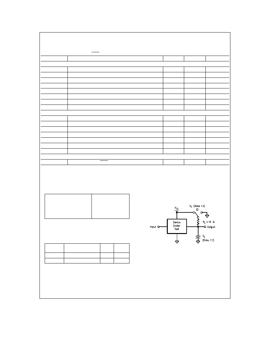
AC Test Conditions
Input Pulse Levels
GND to 3 0V
Input Rise and Fall Times
6 ns (10% ≠ 90%)
Input and Output
1 3V
Reference Levels
TRI-STATE Reference
Active High
a
0 5V
Levels (Note 12)
Active Low
b
0 5V
Note 11
C
L
e
100 pF includes jig and scope capacitance
Note 12
S1
e
V
CC
for active low to high impedance measurements
S1
e
GND for active high to high impedance measurements
S1
e
open for all other timing measurements
Capacitance
(T
A
e
25 C f
e
1 MHz)
Symbol
Parameter
Typ
Units
(Note 13)
C
IN
Input Capacitance
5
pF
C
OUT
Output Capacitance
7
pF
Note 13
This parameter is not 100% tested
Note 14
Output rise and fall times 25 ns max (10%≠90%) with 100 pF load
TL F 9980 ≠ 2
3
8572AM
Military Version
Absolute Maximum Ratings
(Notes 1
2)
The 883 specifications are written to reflect the current
(at the time of printing) Rel Electrical Test Specifica-
tions (RETS) established by National Semiconductor for
this product For a copy of the latest version of the
RETS please contact your local National Semiconduc-
tor sales office or distributor
Supply Voltage (V
CC
)
b
0 5V to
a
7 0V
DC Input Voltage (V
IN
)
b
0 5V to V
CC
a
0 5V
DC Output Voltage (V
OUT
)
b
0 5V to V
CC
a
0 5V
Storage Temperature Range
b
65 C to
a
150 C
Power Dissipation (PD)
500 mW
Lead Temperature (Soldering 10 sec )
260 C
Operation Conditions
Min
Max
Unit
Supply Voltage (V
CC
) (Note 3)
4 5
5 5
V
Supply Voltage (V
BB
) (Note 3)
2 2 V
CC
b
0 4
V
DC Input or Output Voltage
0 0
V
CC
V
(V
IN
V
OUT
)
Operating Temperature (T
A
)
b
55
a
125
C
Electro-Static Discharge Rating
1
kV
Typical Values
i
JA
DIP
Board
45 C W
Socket
52 C W
DC Electrical Characteristics
V
CC
e
5 0V
g
10% V
BB
e
3V
Symbol
Parameter
V
CC
Conditions
Min
Max
Units
V
IH
High Level Input Voltage
All Inputs Except OSC IN
2 0
V
(Note 4)
OSC IN with External Clock
V
BB
b
0 1
V
V
IL
Low Level Input Voltage
All Inputs Except OSC IN
0 8
V
OSC IN with External Clock
0 1
V
V
OH
High Level Output Voltage
5 5V
I
OUT
e b
20 mA
V
CC
b
0 1
V
(Excluding OSC OUT)
5 5V
I
OUT
e b
4 0 mA
3 5
V
V
OL
Low Level Output Voltage
5 5V
I
OUT
e
20 mA
0 1
V
(Excluding OSC OUT)
5 5V
I
OUT
e
4 0 mA
0 25
V
I
IN
Input Current (Except OSC IN)
5 5V
V
IN
e
V
CC
or GND
g
1 0
m
A
I
OZ
Output TRI-STATE Current
5 5V
V
OUT
e
V
CC
or GND
g
5 0
m
A
I
CC
Quiescent Supply Current
F
OSC
e
32 768 kHz
275
m
A
(Note 7)
5 5V
V
IN
e
V
CC
or GND (Note 5)
1 0
mA
5 5V
V
IN
e
V
CC
or GND (Note 6)
12 0
mA
5 5V
V
IN
e
V
IH
or V
IL
(Note 6)
F
OSC
e
4 9152 MHz
8
mA
5 5V
V
IN
e
V
CC
or GND (Note 6)
20
mA
5 5V
V
IN
e
V
IH
or V
IL
(Note 6)
I
CC
Quiescent Supply Current
V
BB
e
GND V
IN
e
V
CC
or GND
(Single Supply Mode)5 5V
F
OSC
e
32 768 kHz
40
m
A
(Note 7)
5 5V
F
OSC
e
4 9152 MHz
7 5
mA
I
BB
Standby Mode Battery
OSC OUT
e
Open Circuit
Supply Current
Other Pins
e
GND
(Note 7)
0V
F
OSC
e
32 768 kHz
10
m
A
0V
F
OSC
e
4 9152 MHz
400
m
A
I
BLK
Battery Leakage
2 2V
s
V
BB
s
4 0V
5 5V
25 C
b
5
1 5
m
A
5 5V
b
55 C
b
5
3 5
m
A
5 5V
a
125 C
b
5
3 5
m
A
Note 1
Absolute Maximum Ratings are those values beyond which damage to the device may occur
Note 2
Unless otherwise specified all voltages are referenced to ground
Note 3
For F
OSC
e
4 194304 or 4 9152 MHz V
BB
minimum
e
2 8V In battery backed mode V
BB
s
V
CC
b
0 4V
Single Supply Mode Data retention voltage is 2 2V min
In single Supply Mode (Power connected to V
CC
pin) 4 5V
s
V
CC
s
5 5V
Note 4
This parameter (V
IH
) is not tested on all pins at the same time
Note 5
This specification tests I
CC
with all power fail circuitry disabled by setting D7 of Interrupt Control Register 1 to 0
Note 6
This specification tests I
CC
with all power fail circuitry enabled by setting D7 of Interrupt Control Register 1 to 1
Note 7
OSC IN is driven by a signal generator Contents of the Test Register
e
00(H) and the MFO pin is not configured as buffered oscillator out
4

8572AM
Military Version
AC Electrical Characteristics
V
CC
e
4 5V and 5 5V V
BB
e
3V V
PFAIL
l
V
IH
C
L
e
100 pF (unless otherwise specified)
Symbol
Parameter
Min
Max
Units
READ TIMING
t
AR
Address Valid Prior to Read Strobe
20
ns
t
RW
Read Strobe Width (Note 8)
80
ns
t
CD
Chip Select to Data Valid Time
80
ns
t
RD
Read Strobe to Valid Data
70
ns
t
DZ
Read or Chip Select to TRI-STATE
60
ns
t
RCH
Chip Select Hold after Read Strobe
0
ns
t
DS
Minimum Inactive Time between Read or Write Accesses
50
ns
WRITE TIMING
t
AW
Address Valid before Write Strobe
20
ns
t
CW
Chip Select to End of Write Strobe
90
ns
t
WW
Write Strobe Width (Note 9)
80
ns
t
DW
Data Valid to End of Write Strobe
50
ns
t
WCH
Chip Select Hold after Write Strobe
0
ns
Note 8
Read Strobe width as used in the read timing table is defined as the period when both chip select and read inputs are low Hence read commences when
both signals are low and terminates when either signal returns high
Note 9
Write Strobe width as used in the write timing table is defined as the period when both chip select and write inputs are low Hence write commences when
both signals are low and terminates when either signal returns high
AC Test Conditions
Input Pulse Levels
GND to 3 0V
Input Rise and Fall Times
6 ns (10% ≠ 90%)
Input and Output
1 3V
Reference Levels
TRI-STATE Reference
Active High
a
0 5V
Levels (Note 11)
Active Low
b
0 5V
Note 10
C
L
e
100 pF includes jig and scope capacitance
Note 11
S1
e
V
CC
for active low to high impedance measurements
S1
e
GND for active high to high impedance measurements
S1
e
open for all other timing measurements
Capacitance
(T
A
e
25 C f
e
1 MHz)
Symbol
Parameter
Typ
Units
(Note 12)
C
IN
Input Capacitance
5
pF
C
OUT
Output Capacitance
7
pF
Note 12
This parameter is not 100% tested
Note 13
Output rise and fall times 25 ns max (10%≠90%) with 100 pF load
TL F 9980 ≠ 24
5