 | –≠–ª–µ–∫—Ç—Ä–æ–Ω–Ω—ã–π –∫–æ–º–ø–æ–Ω–µ–Ω—Ç: DS0026 | –°–∫–∞—á–∞—Ç—å:  PDF PDF  ZIP ZIP |
DS0026
Dual High-Speed MOS Driver
General Description
DS0026 is a low cost monolithic high speed two phase MOS
clock driver and interface circuit. Unique circuit design pro-
vides both very high speed operation and the ability to drive
large capacitive loads. The device accepts standard TTL out-
puts and converts them to MOS logic levels. The device may
be driven from standard 54/74 series and 54S/74S series
gates and flip-flops or from drivers such as the DS8830 or
DM7440. The DS0026 is intended for applications in which
the output pulse width is logically controlled; i.e., the output
pulse width is equal to the input pulse width.
The DS0026 is designed to fulfill a wide variety of MOS inter-
face requirements. Information on the correct usage of the
DS0026 in these as well as other systems is included in the
application note AN-76.
Features
n
Fast rise and fall times -- 20 ns 1000 pF load
n
High output swing -- 20V
n
High output current drive --
±
1.5 amps
n
TTL compatible inputs
n
High rep rate -- 5 to 10 MHz depending on power
dissipation
n
Low power consumption in MOS "0" state -- 2 mW
n
Drives to 0.4V of GND for RAM address drive
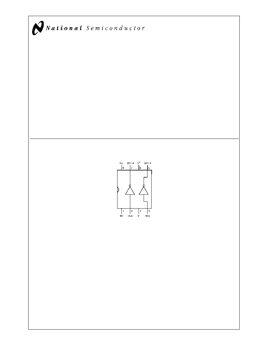
Connection Diagrams (Top Views)
Dual-In-Line Package
DS005853-2
Order Number DS0026CN
See NS Package Number N08E
February 2000
DS0026
Dual
High-Speed
MOS
Driver
© 2000 National Semiconductor Corporation
DS005853
www.national.com
Absolute Maximum Ratings
(Note 1)
If Military/Aerospace specified devices are required,
please contact the National Semiconductor Sales Office/
Distributors for availability and specifications.
V
+
- V
-
Differential Voltage
22V
Input Current
100 mA
Input Voltage (V
IN
- V
-
)
5.5V
Peak Output Current
1.5A
Maximum Power Dissipation
*
at T
A
=
25∞C
420mW
Operating Temperature Range
0∞C to +70∞C
Storage Temperature Range
-65∞C to +150∞C
Lead Temperature
(Soldering, 10 sec.)
300∞C
Note:
*
Derate N08E package 9.3 mW/∞C for T
A
above 25∞C.
J
A
= 107∞C/W
Electrical Characteristics
(Notes 2, 3, 4)
Symbol
Parameter
Conditions
Min
Typ
Max
Units
V
IH
Logic "1" Input Voltage
V
-
= 0V
2
1.5
V
I
IH
Logic "1" Input Current
V
IN
- V
-
= 2.4V
10
15
mA
V
IL
Logic "0" Input Voltage
V
-
= 0V
0.6
0.4
V
I
IL
Logic "0" Input Current
V
IN
- V
-
= 0V
-3
-10
µA
V
OL
Logic "1" Output Voltage
V
IN
- V
-
= 2.4V, I
OL
= 1 mA
V
-
+0.7
V
-
+1.0
V
V
OH
Logic "0" Output Voltage
V
IN
- V
-
= 0.4V, V
SS
V
+
+ 1.0V
I
OH
= - 1 mA
V
+
- 1.0
V
+
-0.8
V
I
CC(ON)
"ON" Supply Current
(one side on)
V
+
- V
-
= 20V, V
IN
- V
-
= 2.4V
30
40
mA
I
CC(OFF)
"OFF" Supply Current
V
+
- V
-
= 20V,
V
IN
- V
-
= 0V
10
100
µA
Switching Characteristics
(T
A
= 25∞C) (Notes 5, 6)
Symbol
Parameter
Conditions
Min
Typ
Max
Units
t
ON
Turn-On Delay
(Figure 1)
5
7.5
12
ns
(Figure 2)
11
ns
t
OFF
Turn-Off Delay
(Figure 1)
12
15
ns
(Figure 2)
13
ns
t
r
Rise Time
(Figure 1),
(Note 5)
C
L
= 500 pF
15
18
ns
C
L
= 1000 pF
20
35
ns
(Figure 2),
(Note 5)
C
L
= 500 pF
30
40
ns
C
L
= 1000 pF
36
50
ns
t
f
Fall Time
(Figure 1),
(Note 5)
C
L
= 500 pF
12
16
ns
C
L
= 1000 pF
17
25
ns
(Figure 2),
(Note 5)
C
L
= 500 pF
28
35
ns
C
L
= 1000 pF
31
40
ns
Note 1: "Absolute Maximum Ratings" are those values beyond which the safety of the device cannot be guaranteed. Except for "Operating Temperature Range" they
are not meant to imply that the devices should be operated at these limits. The table of "Electrical Characteristics provides conditions for actual device operation.
Note 2: These specifications apply for V
+
- V
-
= 10V to 20V, C
L
= 1000 pF, over the temperature range of 0∞C to +70∞C for the DS0026CN.
Note 3: All currents into device pins shown as positive, out of device pins as negative, all voltages referenced to ground unless otherwise noted. All values shown
as max or min on absolute value basis.
Note 4: All typical values for T
A
= 25∞C.
Note 5: Rise and fall time are given for MOS logic levels; i.e., rise time is transition from logic "0" to logic "1" which is voltage fall.
Note 6: The high current transient (as high as 1.5A) through the resistance of the internal interconnecting V
-
lead during the output transition from the high state to
the low state can appear as negative feedback to the input. If the external interconnecting lead from the driving circuit to V
-
is electrically long, or has significant dc
resistance, it can subtract from the switching response.
DS0026
www.national.com
2

Typical V
BB
Connection
Typical Performance Characteristics
DS005853-8
Input Current vs Input Voltage
DS005853-22
Supply Current vs Temperature
DS005853-23
Turn-On and Turn-Off Delay
vs Temperature
DS005853-24
Rise Time vs Load
Capacitance
DS005853-25
Fall Time vs Load
Capacitance
DS005853-26
DS0026
www.national.com
3
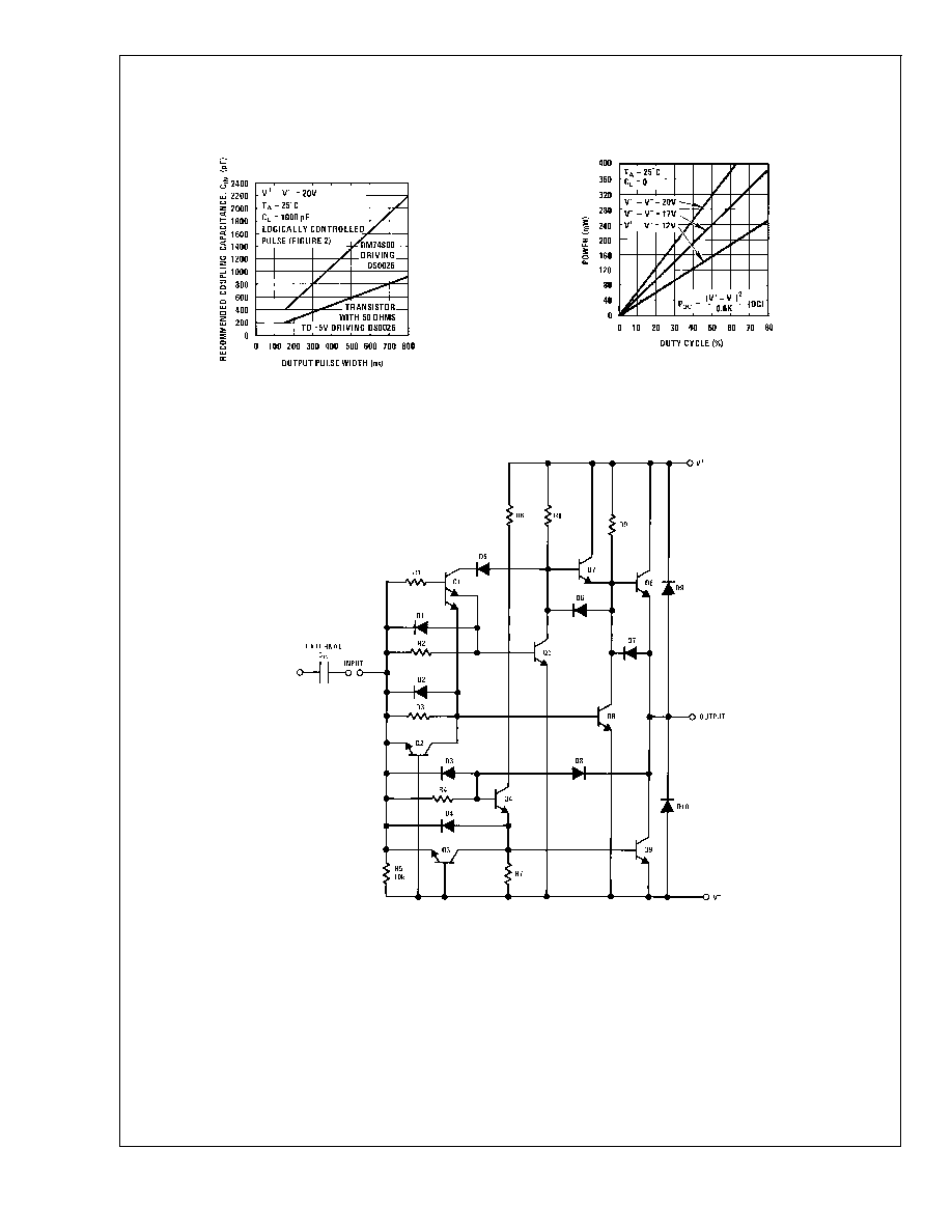
Typical Performance Characteristics
(Continued)
Schematic Diagram
Recommended Input Coding
Capacitance
DS005853-27
DC Power (P
DC
) vs
Duty Cycle
DS005853-28
1/2 DS0026
DS005853-10
DS0026
www.national.com
4
AC Test Circuits and Switching Time Waveforms
Typical Applications
Application Hints
DRIVING THE MM5262 WITH THE
DS0026 CLOCK DRIVER
The clock signals for the MM5262 have three requirements
which have the potential of generating problems for the user.
These requirements, high speed, large voltage swing and
large capacitive loads, combine to provide ample opportunity
for inductive ringing on clock lines, coupling clock signals to
other clocks and/or inputs and outputs and generating noise
on the power supplies. All of these problems have the poten-
tial of causing the memory system to malfunction. Recogniz-
ing the source and potential of these problems early in the
design of a memory system is the most critical step. The ob-
ject here is to point out the source of these problems and
give a quantitative feel for their magnitude.
Line ringing comes from the fact that at a high enough fre-
quency any line must be considered as a transmission line
with distributed inductance and capacitance. To see how
much ringing can be tolerated we must examine the clock
voltage specification.
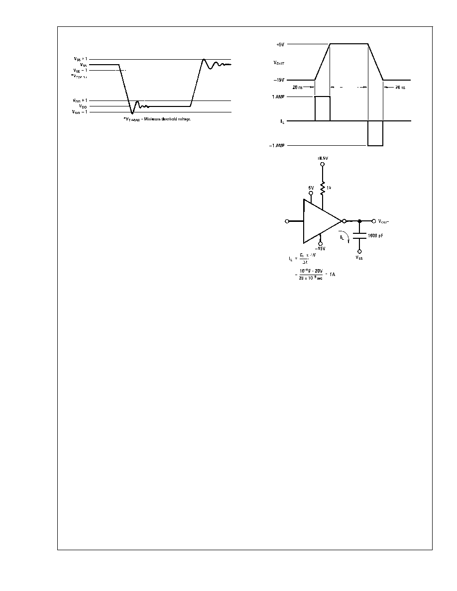
Figure 3 shows the clock specification,
in diagram form, with idealized ringing sketched in. The ring-
ing of the clock about the V
SS
level is particularly critical. If
the V
SS
- 1 V
OH
is not maintained, at
all times, the informa-
tion stored in the memory could be altered. Referring to
Fig-
ure 1, if the threshold voltage of a transistor were -1.3V, the
clock going to V
SS
- 1 would mean that all the devices,
whose gates are tied to that clock, would be only 300 mV
from turning on. The internal circuitry needs this noise mar-
gin and from the functional description of the RAM it is easy
to see that turning a clock on at the wrong time can have di-
sastrous results.
DS005853-12
DS005853-13
FIGURE 1.
DS005853-14
DS005853-15
FIGURE 2.
AC Coupled MOS Clock Driver
DS005853-16
DC Coupled RAM Memory Address or Precharge
Driver (Positive Supply Only)
DS005853-17
DS0026
www.national.com
5
Application Hints
(Continued)
Controlling the clock ringing is particularly difficult because of
the relative magnitude of the allowable ringing, compared to
magnitude of the transition. In this case it is 1V out of 20V or
only 5%. Ringing can be controlled by damping the clock
driver and minimizing the line inductance.
Damping the clock driver by placing a resistance in series
with its output is effective, but there is a limit since it also
slows down the rise and fall time of the clock signal. Because
the typical clock driver can be much faster than the worst
case driver, the damping resistor serves the useful function
of limiting the minimum rise and fall time. This is very impor-
tant because the faster the rise and fall times, the worse the
ringing problem becomes. The size of the damping resistor
varies because it is dependent on the details of the actual
application. It must be determined empirically. In practice a
resistance of 10
to 20
is usually optimum.
Limiting the inductance of the clock lines can be accom-
plished by minimizing their length and by laying out the lines
such that the return current is closely coupled to the clock
lines. When minimizing the length of clock lines it is impor-
tant to minimize the distance from the clock driver output to
the furthest point being driven. Because of this, memory
boards are usually designed with clock drivers in the center
of the memory array, rather than on one side, reducing the
maximum distance by a factor of 2.
Using multilayer printed circuit boards with clock lines sand-
wiched between the V
DD
and V
SS
power plains minimizes
the inductance of the clock lines. It also serves the function
of preventing the clocks from coupling noise into input and
output lines. Unfortunately multilayer printed circuit boards
are more expensive than two sided boards. The user must
make the decision as to the necessity of multilayer boards.
Suffice it to say here, that reliable memory boards can be de-
signed using two sided printed circuit boards.
Because of the amount of current that the clock driver must
supply to its capacitive load, the distribution of power to the
clock driver must be considered.
Figure 4 gives the idealized
voltage and current waveforms for a clock driver driving a
1000 pF capacitor with 20 ns rise and fall time.
As can be seen the current is significant. This current flows
in the V
DD
and V
SS
power lines. Any significant inductance in
the lines will produce large voltage transients on the power
supplies. A bypass capacitor, as close as possible to the
clock driver, is helpful in minimizing this problem. This by-
pass is most effective when connected between the V
SS
and
V
DD
supplies. The size of the bypass capacitor depends on
the amount of capacitance being driven. Using a low induc-
tance capacitor, such as a ceramic or silver mica, is most ef-
fective. Another helpful technique is to run the V
DD
and V
SS
lines, to the clock driver, adjacent to each other. This tends to
reduce the lines inductance and therefore the magnitude of
the voltage transients.
While discussing the clock driver, it should be pointed out
that the DS0026 is a relatively low input impedance device.
It is possible to couple current noise into the input without
seeing a significant voltage. Since the noise is difficult to de-
tect with an oscilloscope it is often overlooked.
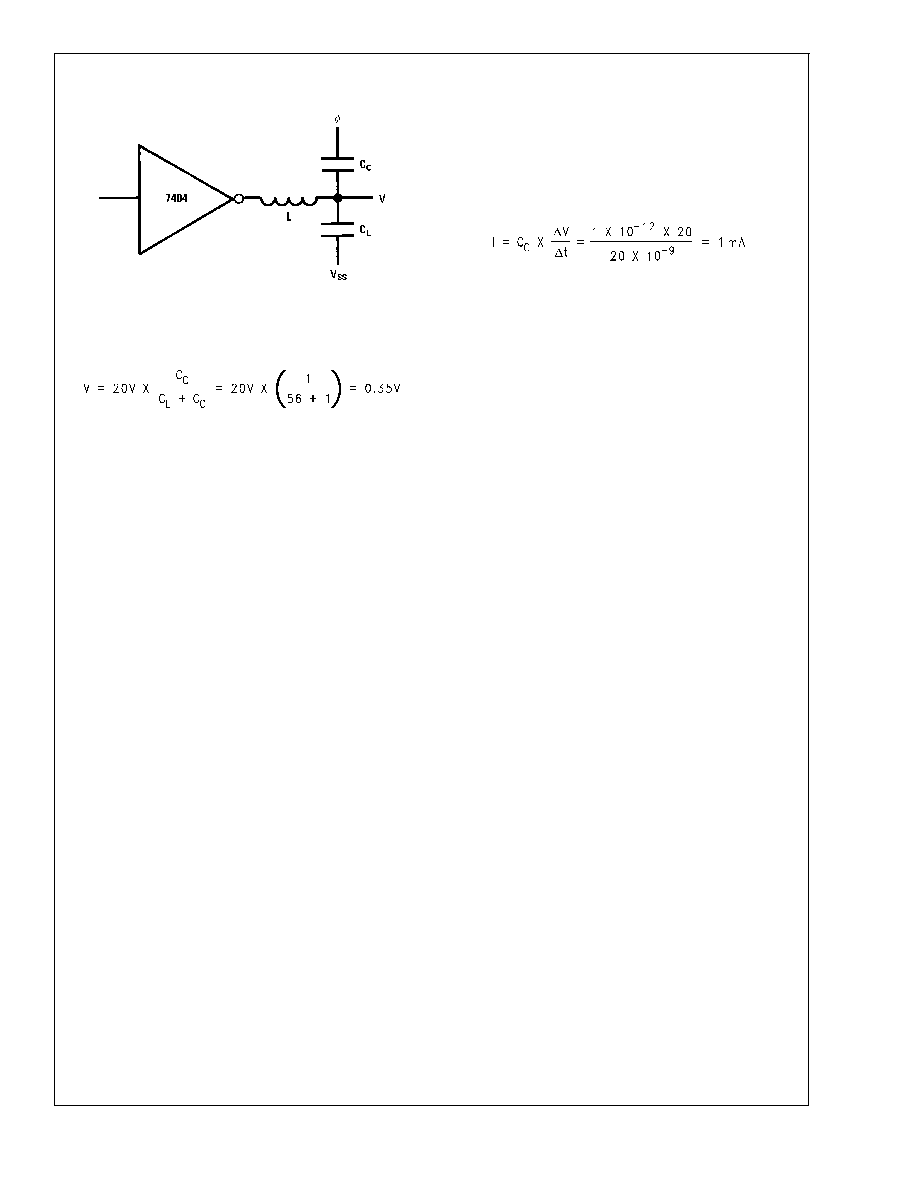
Lastly, the clock lines must be considered as noise genera-
tors.
Figure 5 shows a clock coupled through a parasitic cou-
pling capacitor, C
C
, to eight data input lines being driven by
a 7404. A parasitic lumped line inductance, L, is also shown.
Let us assume, for the sake of argument, that C
C
is 1 pF and
that the rise time of the clock is high enough to completely
isolate the clock transient from the 7404 because of the in-
ductance, L.
DS005853-18
FIGURE 3. Clock Waveform
DS005853-19
FIGURE 4. Clock Waveforms (Voltage and Current)
DS0026
www.national.com
6
Application Hints
(Continued)
With a clock transition of 20V the magnitude of the voltage
generated across C
L
is:
This has been a hypothetical example to emphasize that
with 20V low rise/fall time transitions, parasitic elements can
not be neglected. In this example, 1 pF of parasitic capaci-
tance could cause system malfunction, because a 7404
without a pull up resistor has typically only 0.3V of noise mar-
gin in the "1" state at 25∞C. Of course it is stretching things to
assume that the inductance, L, completely isolates the clock
transient from the 7404. However, it does point out the need
to minimize inductance in input/output as well as clock lines.
The output is current, so it is more meaningful to examine
the current that is coupled through a 1 pF parasitic capaci-
tance. The current would be:
This exceeds the total output current swing so it is obviously
significant.
Clock coupling to inputs and outputs can be minimized by
using multilayer printed circuit boards, as mentioned previ-
ously, physically isolating clock lines and/or running clock
lines at right angles to input/output lines. All of these tech-
niques tend to minimize parasitic coupling capacitance from
the clocks to the signals in question.
In considering clock coupling it is also important to have a
detailed knowledge of the functional characteristics of the
device being used. As an example, for the MM5262, cou-
pling noise from the
2 clock to the address lines is of no par-
ticular consequence. On the other hand the address inputs
will be sensitive to noise coupled from
1 clock.
DS005853-20
FIGURE 5. Clock Coupling
DS0026
www.national.com
7
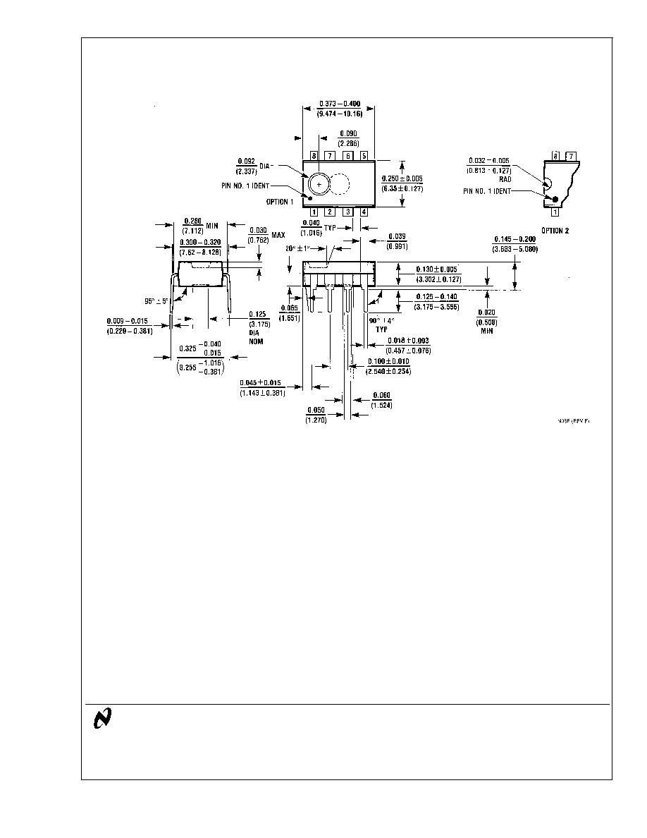
Packaging Information
Physical Dimensions
inches (millimeters) unless otherwise noted
LIFE SUPPORT POLICY
NATIONAL'S PRODUCTS ARE NOT AUTHORIZED FOR USE AS CRITICAL COMPONENTS IN LIFE SUPPORT
DEVICES OR SYSTEMS WITHOUT THE EXPRESS WRITTEN APPROVAL OF THE PRESIDENT AND GENERAL
COUNSEL OF NATIONAL SEMICONDUCTOR CORPORATION. As used herein:
1. Life support devices or systems are devices or
systems which, (a) are intended for surgical implant
into the body, or (b) support or sustain life, and
whose failure to perform when properly used in
accordance with instructions for use provided in the
labeling, can be reasonably expected to result in a
significant injury to the user.
2. A critical component is any component of a life
support device or system whose failure to perform
can be reasonably expected to cause the failure of
the life support device or system, or to affect its
safety or effectiveness.
National Semiconductor
Corporation
Americas
Tel: 1-800-272-9959
Fax: 1-800-737-7018
Email: support@nsc.com
National Semiconductor
Europe
Fax: +49 (0) 180-530 85 86
Email: europe.support@nsc.com
Deutsch Tel: +49 (0) 69 9508 6208
English
Tel: +44 (0) 870 24 0 2171
FranÁais Tel: +33 (0) 1 41 91 8790
National Semiconductor
Asia Pacific Customer
Response Group
Tel: 65-2544466
Fax: 65-2504466
Email: ap.support@nsc.com
National Semiconductor
Japan Ltd.
Tel: 81-3-5639-7560
Fax: 81-3-5639-7507
www.national.com
Molded Dual-In-Line Package (N)
Order Number DS0026CN
NS Package Number N08E
DS0026
Dual
High-Speed
MOS
Driver
National does not assume any responsibility for use of any circuitry described, no circuit patent licenses are implied and National reserves the right at any time without notice to change said circuitry and specifications.