 | –≠–ª–µ–∫—Ç—Ä–æ–Ω–Ω—ã–π –∫–æ–º–ø–æ–Ω–µ–Ω—Ç: DS14196WM | –°–∫–∞—á–∞—Ç—å:  PDF PDF  ZIP ZIP |
DS14196
EIA/TIA-232 5 Driver x 3 Receiver
General Description
The DS14196 is a five driver, three receiver device which
conforms to the EIA/TIA-232-E and the ITU-T V.28 stan-
dards.
The flow-through pinout facilitates simple non-crossover
board layout. The DS14196 provides a peripheral side
one-chip solution for the common 9-pin serial RS-232 inter-
face between data terminals and data communications
equipment.
The DS14196 offers optimum performance when used with
the DS14185 3 x 5 Driver/Receiver, a host side one-chip so-
lution for the common 9-pin serial RS-232 interface between
data terminals and data communications equipment.
Features
n
Replaces two 1488s and one 1489
n
Conforms to EIA/TIA-232-E and ITU-T V.28
n
5 drivers and 3 receivers
n
Flow-through pinout
n
Failsafe receiver outputs high when inputs open
n
20-pin wide SOIC package
n
LapLink
Æ
compatible -- 230.4 kbps data rate
n
Pin compatible with: SN75196, GD75323
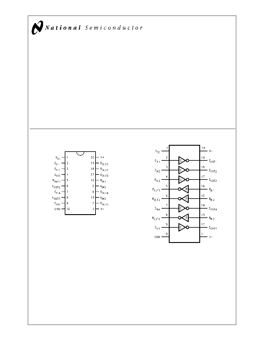
Connection Diagram
Functional Diagram
LapLink
Æ
is a registered trademark of Travelling Software.
SOP
DS012613-1
Order Number DS14196WM
See NS Package Number M20B
DS012613-2
February 2000
DS14196
EIA/TIA-232
5
Drive
r
x
3
Receiver
© 2000 National Semiconductor Corporation
DS012613
www.national.com
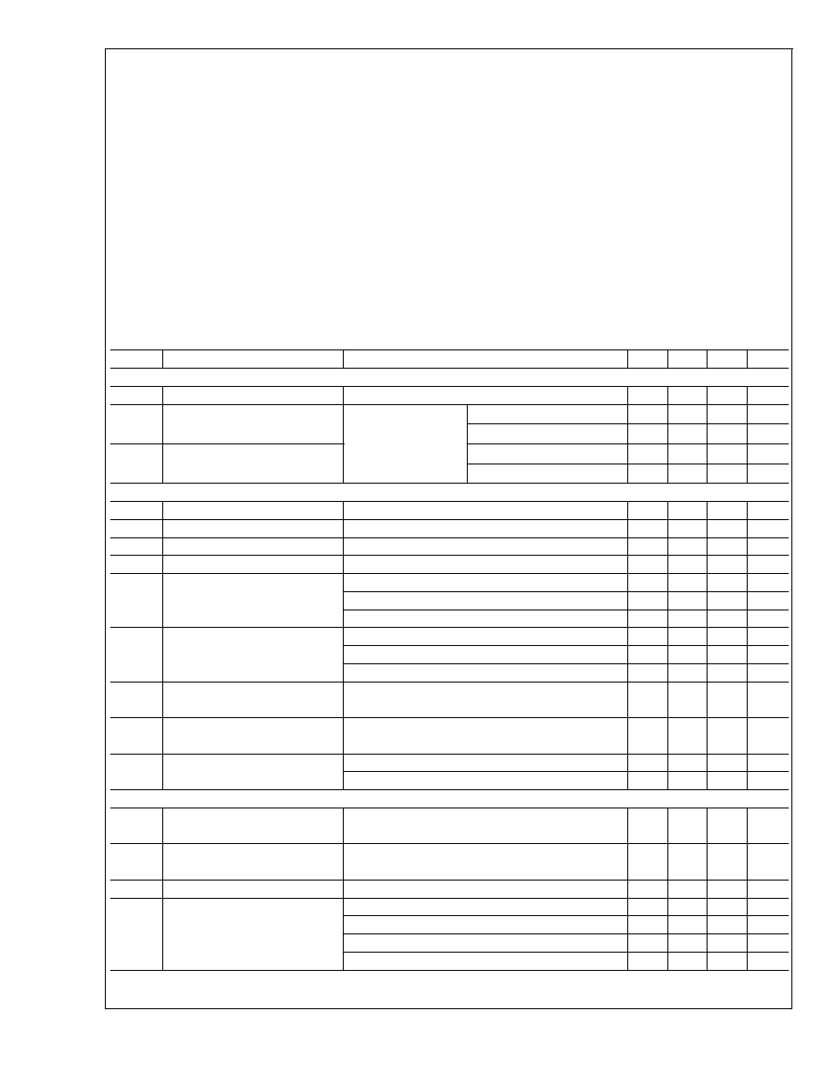
Absolute Maximum Ratings
(Note 1)
If Military/Aerospace specified devices are required,
please contact the National Semiconductor Sales Office/
Distributors for availability and specifications.
Supply Voltage (V
CC
)
+7V
Supply Voltage (V
+
)
+15V
Supply Voltage (V
-
)
-15V
Driver Input Voltage
0V to V
CC
Driver Output Voltage (Power Off)
±
15V
Receiver Input Voltage
±
25V
Receiver Output Voltage (R
OUT
)
0V to V
CC
Maximum Power Package Dissipation
@
+25∞C
M Package
1524 mW
Derate M Package
12.2 mW/∞C above 25∞C
Storage Temperature Range
-65∞C to +150∞C
Lead Temperature Range (Soldering, 4 sec.)
+260∞C
ESD Ratings (HBM. 1.5 k
, 100 pF)
1.5 kV
Recommended Operating
Conditons
Min
Nom
Max
Units
Supply Voltage (V
CC
)
+4.75
+5.0
+5.25
V
Supply Voltage (V
+
)
+9.0
+12.0
+13.2
V
Supply Voltage (V
-
)
-13.2
-12.0
-9.0
V
Operating Free Air
Temperature (T
A
)
0
+25
+70
∞C
Electrical Characteristics
(Note 2) (Note 3)
Over recommended operating supply and temperature ranges unless otherwise specified
Symbol
Parameter
Conditions
Min
Typ
Max
Units
DEVICE CHARACTERISTICS
I
CC
V
CC
Supply Current
No Load, All Inputs at +5V
13
22
mA
I
+
V
+
Supply Current
No Load, All Driver
Inputs at 0.8V or
+2V. All Receiver
Inputs at 0.8V or
2.4V.
V
+
= +9V, V
-
= -9V
16
26
mA
V
+
= +13.2V, V
-
= -13.2V
23
36
mA
I
-
V
-
Supply Current
V
+
= +9V, V
-
= -9V
-18
-26
mA
V
+
= +13.2V, V
-
= -13.2V
-25
-36
mA
DRIVER CHARACTERISTICS
V
IH
High Level Input Voltage
2.0
V
V
IL
Low Level Input Voltage
0.8
V
I
IH
High Level Input Current
V
IN
= 5V
10
µA
I
IL
Low Level Input Current
V
IN
= 0V
-1.1
-1.5
mA
V
OH
High Level Output Voltage
R
L
= 3 k
, V
IN
= 0.8V, V
+
= +9V, V
-
= -9V
6
7
V
R
L
= 3 k
, V
IN
= 0.8V, V
+
= +12V, V
-
= -12V
8
9
V
R
L
= 7 k
, V
IN
= 0.8V, V
+
= +13.2V, V
-
= -13.2V
10
11.5
V
V
OL
Low Level Output Voltage
R
L
= 3 k
, V
IN
= 2V, V
+
= +9V, V
-
= -9V
-7
-6
V
R
L
= 3 k
, V
IN
= 2V, V
+
= +12V, V
-
= -12V
-10
-8
V
R
L
= 7 k
, V
IN
= 2V, V
+
= +13.2V, V
-
= -13.2V
-11.5
-10
V
I
OS
+
Output High Short
V
OUT
= 0V, V
IN
= 0.8V
-6
-12
-18
mA
Circuit Current (Note 4)
I
OS
-
Output Low Short
V
OUT
= 0V, V
IN
= 2.0V
6
12
18
mA
Circuit Current (Note 4)
R
O
Output Resistance
-2V
V
OUT
+2V, V
+
= V
-
= V
CC
= 0V
300
-2V
V
OUT
+2V, V
+
= V
-
= V
CC
= Open Circuit
300
RECEIVER CHARACTERISTICS
V
TH
Input High Threshold
V
OUT
0.4V, I
O
= 3.2 mA
1.85
2.4
V
(Recognized as a High Signal)
V
TL
Input Low Threshold
V
OUT
2.5V, I
O
= -0.5 mA
0.7
1.0
V
(Recognized as a Low Signal)
R
IN
Input Resistance
V
IN
=
±
3V to
±
15V
3.0
3.8
7.0
k
I
IN
Input Current
V
IN
= +15V
2.1
4.0
5.0
mA
V
IN
= +3V
0.43
0.7
1.0
mA
V
IN
= -15V
-2.1
-4.0
-5.0
mA
V
IN
= -3V
-0.43
-0.7
-1.0
mA
DS14196
www.national.com
2
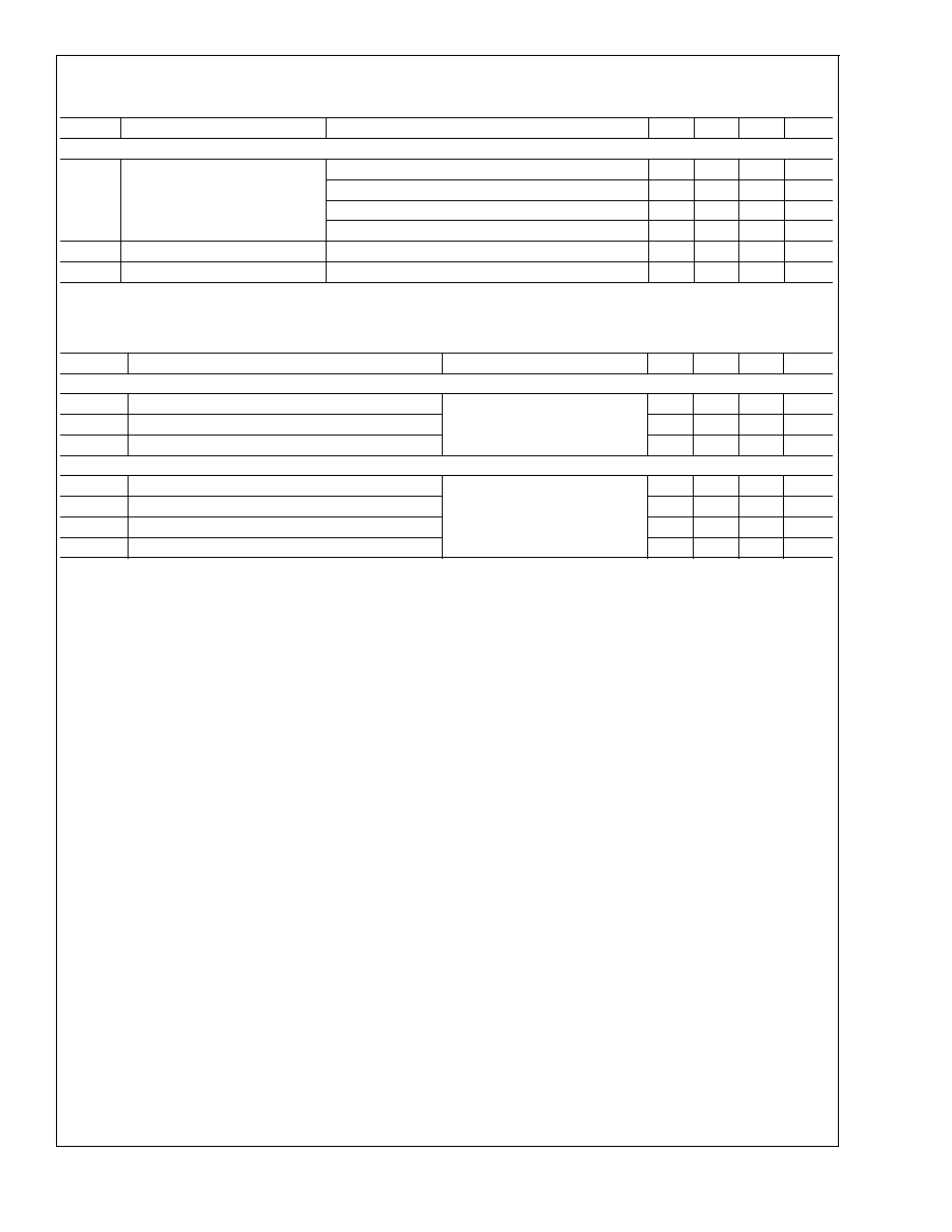
Electrical Characteristics
(Note 2) (Note 3) (Continued)
Over recommended operating supply and temperature ranges unless otherwise specified
Symbol
Parameter
Conditions
Min
Typ
Max
Units
RECEIVER CHARACTERISTICS
V
OH
High Level Output Voltage
(Note 7)
I
OH
= -0.5 mA, V
IN
= -3V
2.6
4.0
V
I
OH
= -10 µA, V
IN
= -3V
4.0
4.9
V
I
OH
= -0.5 mA, V
IN
= Open Circuit
2.6
4.0
V
I
OH
= -10 µA, V
IN
= Open Circuit
4.0
4.9
V
V
OL
Low Level Output Voltage
I
OL
= 3.2 mA, V
IN
= +3V
0.2
0.4
V
I
OSR
Short Circuit Current
V
OUT
= 0V, V
IN
= 0V (Note 4)
-1.7
-2.7
-4
mA
Switching Characteristics
(Note 3) (Note 5) (Note 6)
T
A
= 25∞C
Symbol
Parameter
Conditions
Min
Typ
Max
Units
DRIVER CHARACTERISTICS
t
PHL
Propagation Delay High to Low
R
L
= 3 k
, C
L
= 50 pF
(
Figures 1, 2)
60
350
ns
t
PLH
Propagation Delay Low to High
300
450
ns
t
r
, t
f
Rise/Fall Time (Note 8)
40
ns
RECEIVER CHARACTERISTICS
t
PHL
Propagation Delay High to Low
R
L
= 1.5 k
, C
L
= 15 pF
(includes fixture plus probe),
(
Figures 3, 4)
150
350
ns
t
PLH
Propagation Delay Low to High
240
350
ns
t
r
Rise Time
40
175
ns
t
f
Fall Time
40
100
ns
Note 1: Absolute Maximum Ratings are those values beyond which the safety of the device cannot be guaranteed. They are not meant to imply that the devices
should be operated at these limits. The table of Electrical Characteristics specifies conditions of device operation.
Note 2: Current into device pins is defined as positive. Current out of the device pins is defined as negative. All voltages are referenced to ground unless otherwise
specified. For current, minimum and maximum values are specified as an absolute value and the sign is used to indicate direction. For voltage logic levels, the more
positive value is designated as maximum. For example, if -6V is a maximum, the typical value -6.8V is more negative.
Note 3: All typicals are given for: V
CC
= +5V, V
+
= +12V, V
-
= -12V, T
A
= +25∞C.
Note 4: Only one driver output shorted at a time.
Note 5: Generator characteristics for driver input: f = 64 kHz (128 kbps), t
r
= t
f
<
10 ns, V
IH
= 3V, V
IL
= 0V, duty cycle = 50%.
Note 6: Generator characteristics for receiver input: f = 64 kHz (128 kbps), t
r
= t
f
= 200 ns, V
IH
= 3V, V
IL
= -3V, duty cycle = 50%.
Note 7: If receiver inputs are unconnected, receiver output is a logic high.
Note 8: Refer to typical curves. Driver output slew rate is measured from the +3V to the -3V level on the output waveform. Inputs not under test are connected to
V
CC
or GND. Slew rate is determined by load capacitance. To comply with a 30 V/µs maximum slew rate, a minimum load capacitance of 390 pF is recommended.
DS14196
www.national.com
3
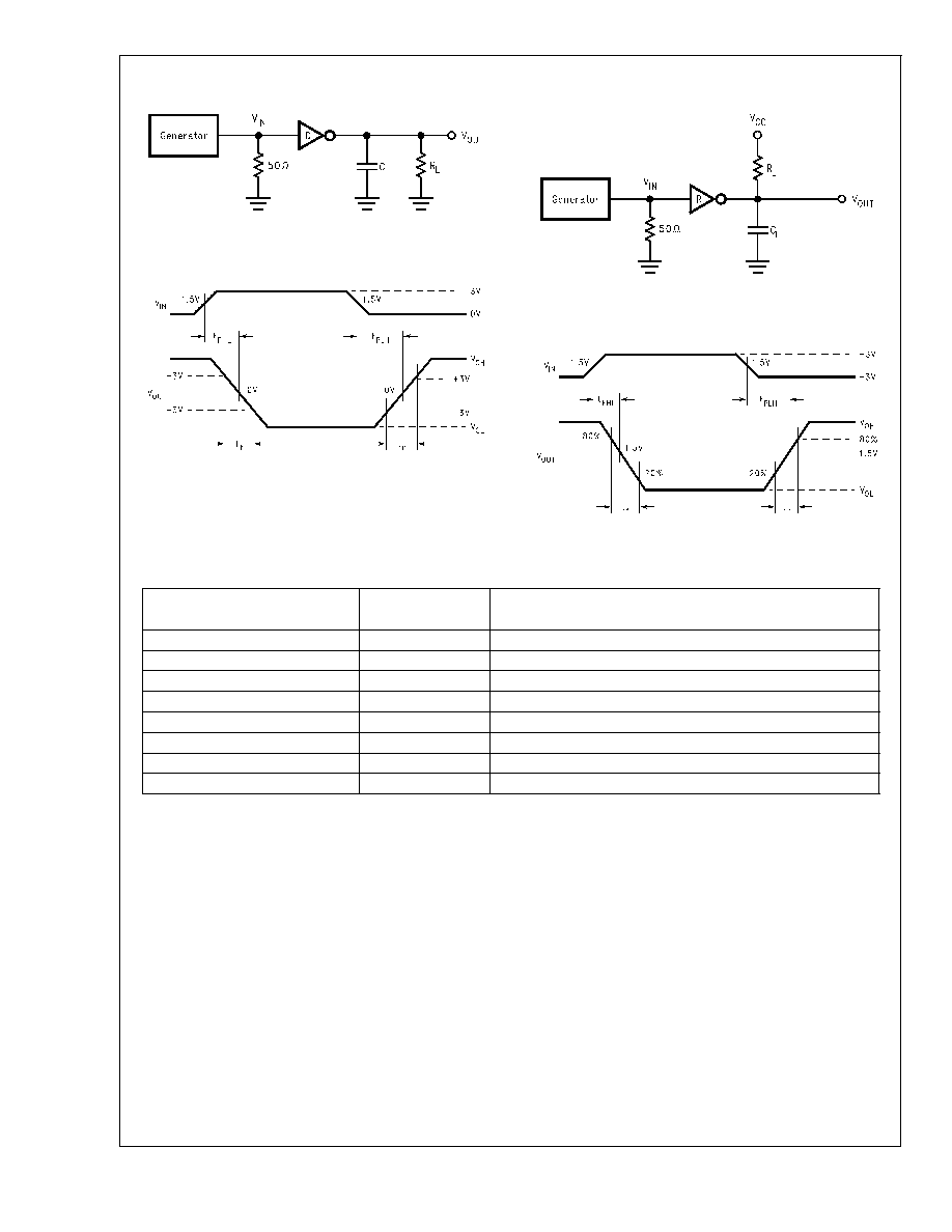
Parameter Measurement Information
Pin Descriptions
Pin #
Pin
Description
Name
2, 3, 4, 7, 9
D
IN
Driver Input Pins
12, 14, 17, 18, 19
D
OUT
Driver Output Pins, RS-232 Levels
13, 15, 16
R
IN
Receiver Input Pins, RS-232 Levels
5, 6, 8
R
OUT
Receiver Output Pins
10
GND
Ground
20
V
+
Positive Power Supply Pin (+9.0
V
+
+13.2)
11
V
-
Negative Power Supply Pin (-9.0
V
-
-13.2)
1
V
CC
Positive Power Supply Pin (+5V
±
5%)
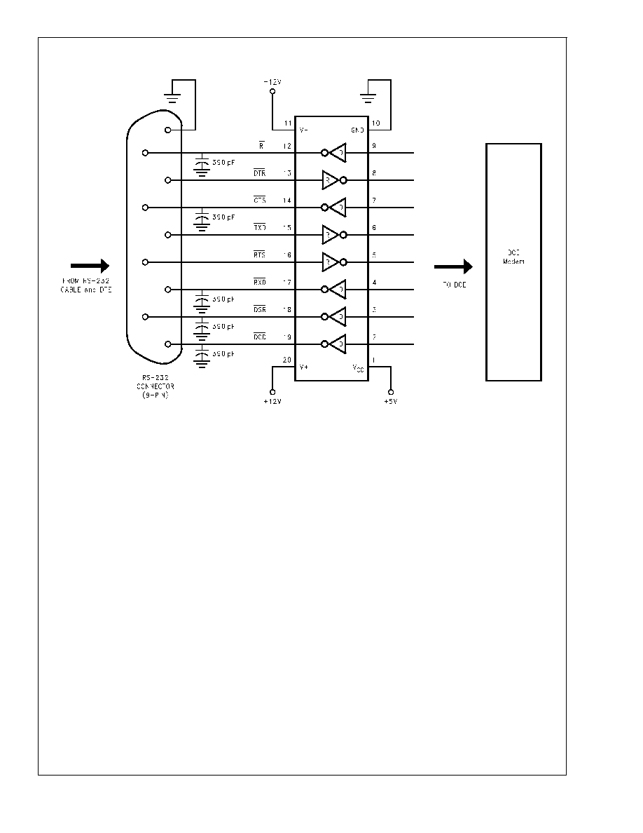
Applications Information
In a typical Data Terminal Equipment (DTE) to Data
Circuit-Terminating Equipment (DCE) 9-pin de-facto inter-
face implementation, 2 data lines and 6 control lines are re-
quired. The data lines are TXD and RXD. The control lines
are RTS, DTR, DSR, DCD, CTS and RI.
The DS14196 is a 5 x 3 Driver/Receiver and offers a single
chip solutuion for this DTE interface. As shown in
Figure 5,
this interface allows for direct flow-thru interconnect. For a
more conservative design, the user may wish to insert
ground traces between the signal lines to minimize cross
talk.
FAILSAFE RECEIVER OUTPUTS
The DS14196 features failsafe receiver outputs. In failsafe
mode, if the receiver input becomes zero or an open-circuit,
the receiver output is pulled to a high level.
LapLink COMPATIBILITY
The DS14196 can easily provide 128 kbps data rate under
maximum driver load conditions of C
L
= 2500 pF and R
L
= 3
k
, while power supplies are:
V
CC
= +4.75V, V
+
= 10.8V, V
-
= -10.8V
MOUSE DRIVING
A typical mouse can be powered from the drivers. Two driver
outputs connected in parallel and set to V
OH
can be used to
supply power to the V
+
pin of the mouse. The third driver out-
put is set to V
OL
to sink the current from the V
-
terminal. Re-
fer to typical curves of V
OUT
/I
OUT
.Typical mouse specifica-
tions are:
10 mA at +6V
5 mA at -6V
DS012613-3
FIGURE 1. Driver Propagation Delay and
Transition Time Test Circuit (Note 5)
DS012613-4
FIGURE 2. Driver Propagation Delay and Transition
Time Waveforms Slew Rate (SR) = 6V/(t
r
or t
f
)
DS012613-5
FIGURE 3. Receiver Propagation Delay and Transition
Time Test Circuit (Note 6)
DS012613-6
FIGURE 4. Receiver Propagation Delay and
Transition Time Waveform
DS14196
www.national.com
4
Applications Information
(Continued)
DS012613-7
FIGURE 5. Typical DCE Application
DS14196
www.national.com
5
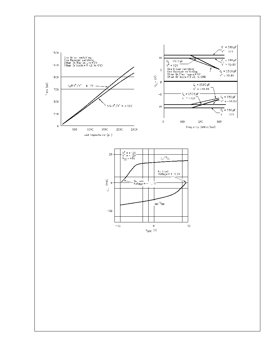
Typical Performance Characteristics
Driver Output Slew Rate between +3V and -3V vs Load
Capacitance
Conditions: V
CC
= 5V, R
L
= 5 k
, T
A
= 25∞C, f
IN
= 64
kHz Square Wave
DS012613-8
Driver Output Voltage vs Frequency and C
L
Conditions: V
CC
= 5V, R
L
= 5 k
, T
A
= 25∞C
DS012613-9
Driver Output Current vs Output Voltage
DS012613-10
DS14196
www.national.com
6
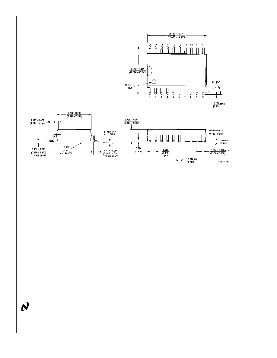
Physical Dimensions
inches (millimeters) unless otherwise noted
LIFE SUPPORT POLICY
NATIONAL'S PRODUCTS ARE NOT AUTHORIZED FOR USE AS CRITICAL COMPONENTS IN LIFE SUPPORT
DEVICES OR SYSTEMS WITHOUT THE EXPRESS WRITTEN APPROVAL OF THE PRESIDENT AND GENERAL
COUNSEL OF NATIONAL SEMICONDUCTOR CORPORATION. As used herein:
1. Life support devices or systems are devices or
systems which, (a) are intended for surgical implant
into the body, or (b) support or sustain life, and
whose failure to perform when properly used in
accordance with instructions for use provided in the
labeling, can be reasonably expected to result in a
significant injury to the user.
2. A critical component is any component of a life
support device or system whose failure to perform
can be reasonably expected to cause the failure of
the life support device or system, or to affect its
safety or effectiveness.
National Semiconductor
Corporation
Americas
Tel: 1-800-272-9959
Fax: 1-800-737-7018
Email: support@nsc.com
National Semiconductor
Europe
Fax: +49 (0) 180-530 85 86
Email: europe.support@nsc.com
Deutsch Tel: +49 (0) 69 9508 6208
English
Tel: +44 (0) 870 24 0 2171
FranÁais Tel: +33 (0) 1 41 91 8790
National Semiconductor
Asia Pacific Customer
Response Group
Tel: 65-2544466
Fax: 65-2504466
Email: ap.support@nsc.com
National Semiconductor
Japan Ltd.
Tel: 81-3-5639-7560
Fax: 81-3-5639-7507
www.national.com
20-Lead (0.300" Wide) Molded Small Outline Package, JEDEC
Order Number DS14196WM
NS Package Number M20B
DS14196
EIA/TIA-232
5
Drive
r
x
3
Receiver
National does not assume any responsibility for use of any circuitry described, no circuit patent licenses are implied and National reserves the right at any time without notice to change said circuitry and specifications.