DS14C535
+5V Supply EIA/TIA-232 3 x 5 Driver/Receiver
General Description
The DS14C535 is three driver, five receiver device which
conforms to EIA/TIA-232-E and CCITT (ITU-T) V.28 stan-
dard specifications. This device employs an internal DC-DC
converter to generate the necessary output levels from a
+5V power supply. A SHUTDOWN (SD) mode reduces the
supply current to 10 µA maximum. In the SD mode, one re-
ceiver is active, allowing ring indicator (RI) to be monitored.
PC Board space consumption is minimized by the availability
of Shrink Small Outline Packaging (SSOP).
The DS14C535 provides a one-chip solution for the common
9-pin serial RS-232 interface between data terminal and
data circuit-terminating equipment.
This device allows an easy migration path to the 3.3V
DS14C335. The packages are the same. The N/C pins on
the DS14C535 are not physically connected to the chip.
Board layout for the DS14C335 will accommodate both de-
vices.
This device's low power requirement and small footprint
makes it an ideal choice for Laptop and Notebook applica-
tions.
Features
n
Pin compatible with DS14C335
n
Conforms to EIA/TIA-232-E and CCITT (ITU-T) V.28
specifications
n
Failsafe receiver outputs high when inputs open
n
Operates with single +5V power supply
n
Low power requirement -- I
CC
12 mA maximum
n
SHUTDOWN mode -- I
CX
10 µA maximum
n
One Receiver (R5) active during SHUTDOWN
n
Operates up to 128 kbps -- Lap-Link
Æ
Compatible
n
4V/µs minimum Slew Rate guaranteed
n
ESD rating of 3 kV on all pins (H, B, M)
n
Available in 28-lead SSOP EIAJ Type II package
n
Only four 0.1 µF capacitors required for the DC-DC
converter
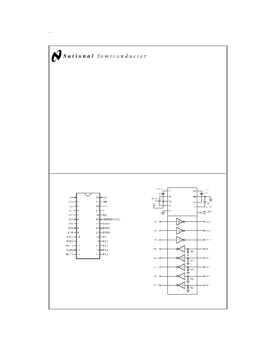
Connection Diagram
Functional Diagram
Lap-Link
Æ
is a registered trademark of Traveling Software Inc.
DS14C535
DS011910-1
Order Number DS14C535MSA
See NS Package Number MSA28
DS011910-2
May 1998
DS14C535
+5V
Supply
EIA/TIA-23
23x5
Driver/Receiver
© 1999 National Semiconductor Corporation
DS011910
www.national.com

Absolute Maximum Ratings
(Note 1)
If Military/Aerospace specified devices are required,
please contact the National Semiconductor Sales Office/
Distributors for availability and specifications.
Supply Voltage (V
CC
)
-0.3V to +6V
V
+
Pin
(V
CC
- 0.3V) to +14V
V
-
Pin
+0.3V to -14V
Input Voltage (D
IN
, SD)
-0.3V to +5.5V
Driver Output Voltage
(V
+
+0.3V) to (V
-
- 0.3V)
Receiver Input Voltage
±
25V
Receiver Output Voltage
- 0.3V to (V
CC
+0.3V)
Junction Temperature
+150∞C
Storage Temperature Range
-65∞C to +150∞C
Lead Temperature (Soldering 4
sec.)
+260∞C
Short Circuit Duration (D
OUT
)
Continuous
Maximum Package Power Dissipation
@
+25∞C
SSOP MSA Package
1286 mW
Derate MSA Package 10.3 mW/∞C above +25∞C
ESD Rating (HBM, 1.5 k
, 100
pF)
3.0 kV
Recommended Operating
Conditions
Min
Max
Units
Supply Voltage (V
CC
)
4.5
5.5
V
Operating Free Air Temperature (T
A
)
DS14C535
0
+70
∞C
DC-DC Converter Capacitors (C1≠C4)
Recommended range of values is 0.1 µF to 0.68 µF,
±
20%.
For more detail refer to application information section of this
data sheet.
Electrical Characteristics
(Notes 2, 3)
Over recommended operating conditions, SD = 0.8V, unless otherwise specified.
Symbol
Parameter
Conditions
Min
Typ
Max
Units
DEVICE CHARACTERISTICS
V
+
Positive Power Supply
No Load
D
IN
= 0.8V
+8.5
V
V
-
Negative Power Supply
C1≠C4 = 0.1 µF
D
IN
= 2.0V
-7.0
V
I
CC
Supply Current
No Load
12
mA
I
CX
SHUTDOWN Supply Current
R
L
= 3 k
, SD = V
CC
1.0
10
µA
V
IH
High Level Enable Voltage
SD
2.0
V
V
IL
Low Level Enable Voltage
GND
0.8
V
I
IH
High Level Enable Current
2.0V
V
IN
5.5V
+2.0
µA
I
IL
Low Level Enable Current
GND
V
IN
0.8V
-2.0
µA
DRIVER CHARACTERISTICS
V
IH
High Level Input Voltage
D
IN
2.0
V
V
IL
Low Level Input Voltage
GND
0.8
V
I
IH
High Level Input Current
2.0V
V
IN
5.5V
+1.0
µA
I
IL
Low Level Input Current
GND
V
IN
0.8V
-1.0
µA
V
OH
High Level Output Voltage
R
L
= 3 k
+5.0
8
V
V
OL
Low Level Output Voltage
-6.7
-5.0
V
I
OS+
Output High Short
V
O
= 0V, V
IN
= 0.8V (Note 7)
-40
-20
-8
mA
Circuit Current
I
OS-
Output Low Short
V
O
= 0V, V
IN
= 2.0V (Note 7)
6
15
40
mA
Circuit Current
R
O
Output Resistance
-2V
V
O
+2V, V
CC
= GND = 0V
300
1200
RECEIVER CHARACTERISTICS (Note 4)
V
TH
Input High Threshold Voltage
R1≠R5, SD = 0.8V (Active Mode)
1.4
2.4
V
R5, 2.0V
SD
5.5V (Shutdown Mode)
2.0
2.8
V
V
TL
Input Low Threshold Voltage
R1≠R5, SD = 0.8V (Active Mode)
0.8
1.1
V
R5, 2.0V
SD
5.5V (Shutdown Mode)
0.8
1.1
V
V
HY
Hysteresis (Note 4)
0.15
1.0
V
R
IN
Input Resistance
V
IN
=
±
3V to
±
15V
3.0
5.4
7.0
k
I
IN
Input Current
V
IN
= +15V
2.14
5.0
mA
V
IN
= +3V
0.43
1.0
mA
V
IN
= -3V
-1.0
-0.43
mA
V
IN
= -15V
-5.0
-2.14
mA
www.national.com
2
Electrical Characteristics
(Notes 2, 3) (Continued)
Over recommended operating conditions, SD = 0.8V, unless otherwise specified.
Symbol
Parameter
Conditions
Min
Typ
Max
Units
RECEIVER CHARACTERISTICS (Note 4)
V
OH
High Level Output Voltage
V
IN
= -3V, I
OH
= -2.0 mA
3.8
V
V
IN
= -3V, I
OH
= -20 µA
4.0
V
V
OL
Low Level Output Voltage
V
IN
= +3V, I
OL
= +2.0 mA
0.23
0.4
V
Switching Characteristics
(Note 4)
Over recommended operating conditions, SD = 0.8V, unless otherwise specified.
Symbol
Parameter
Conditions
Min
Typ
Max
Units
DRIVER CHARACTERISTICS
t
PLH
Propagation Delay LOW to HIGH
R
L
= 3 k
0.1
0.6
1.0
µs
t
PHL
Propagation Delay HIGH to LOW
C
L
= 50 pF
0.1
0.6
1.0
µs
t
SK
Skew |t
PLH
≠t
PHL
|
(
Figures 1, 2)
0
0.2
µs
SR1
Output Slew Rate
R
L
= 3 k
to 7 k
, C
L
= 50 pF (Figure 2)
4
13
30
V/µs
SR2
Output Slew Rate
R
L
= 3 k
, C
L
= 2500 pF (Figure 2)
4
10
30
V/µs
t
PLS
Propagation Delay LOW to SD
(
Figures 5, 6)
0.48
ms
t
PSL
Propagation Delay SD to LOW
R
L
= 3 k
1.88
ms
t
PHS
Propagation Delay HIGH to SD
C
L
= 50 pF
0.62
ms
t
PSH
Propagation Delay SD to HIGH
1.03
ms
RECEIVER CHARACTERISTICS
t
PLH
Propagation Delay LOW to HIGH
C
L
= 50 pF
0.1
0.4
1.0
µs
t
PHL
Propagation Delay HIGH to LOW
(
Figures 3, 4)
0.1
0.6
1.0
µs
t
SK
Skew |t
PLH
≠t
PHL
|
0.1
0.5
µs
t
PLS
Propagation Delay LOW to SD
(
Figures 7, 8)
0.13
µs
t
PSL
Propagation Delay SD to LOW
R
L
= 1 k
1.0
µs
t
PHS
Propagation Delay HIGH to SD
C
L
= 50 pF
0.19
µs
t
PSH
Propagation Delay SD to HIGH
R1≠R4 Only
0.58
µs
Note 1: "Absolute Maximum Ratings" are those values beyond which the safety of the device cannot be guaranteed. They are not meant to imply that the devices
should be operated at these limits. The tables of "Electrical Characteristics" specify conditions for device operation.
Note 2: Typical values are given for V
CC
= 5V and T
A
= +25∞C.
Note 3: Current into device pins is defined as positive. Current out of device pins is defined as negative. All voltages are referenced to ground unless otherwise speci-
fied. For voltage logic levels, the more positive value is designated as maximum. For example, if -5V is a maximum, the typical value (-6.7V) is more negative.
Note 4: Receiver characteristics are guaranteed for SD = 0.8V. When SD = 2.0V, receiver five (R5) is active and meets receiver parameters in SHUTDOWN (SD)
mode, unless otherwise specified.
Note 5: Generator characteristics for driver input: f = 64 kHz (128 kbits/sec), t
r
= t
f
<
10 ns, V
IH
= 3V, V
IL
= 0V, duty cycle = 50%.
Note 6: Generator characteristics for receiver input: f = 64 kHz (128 kbits/sec), t
r
= t
f
<
10 ns, V
IH
= 3V, V
IL
= -3V, duty cycle = 50%.
Note 7: Only one driver output shorted at a time.
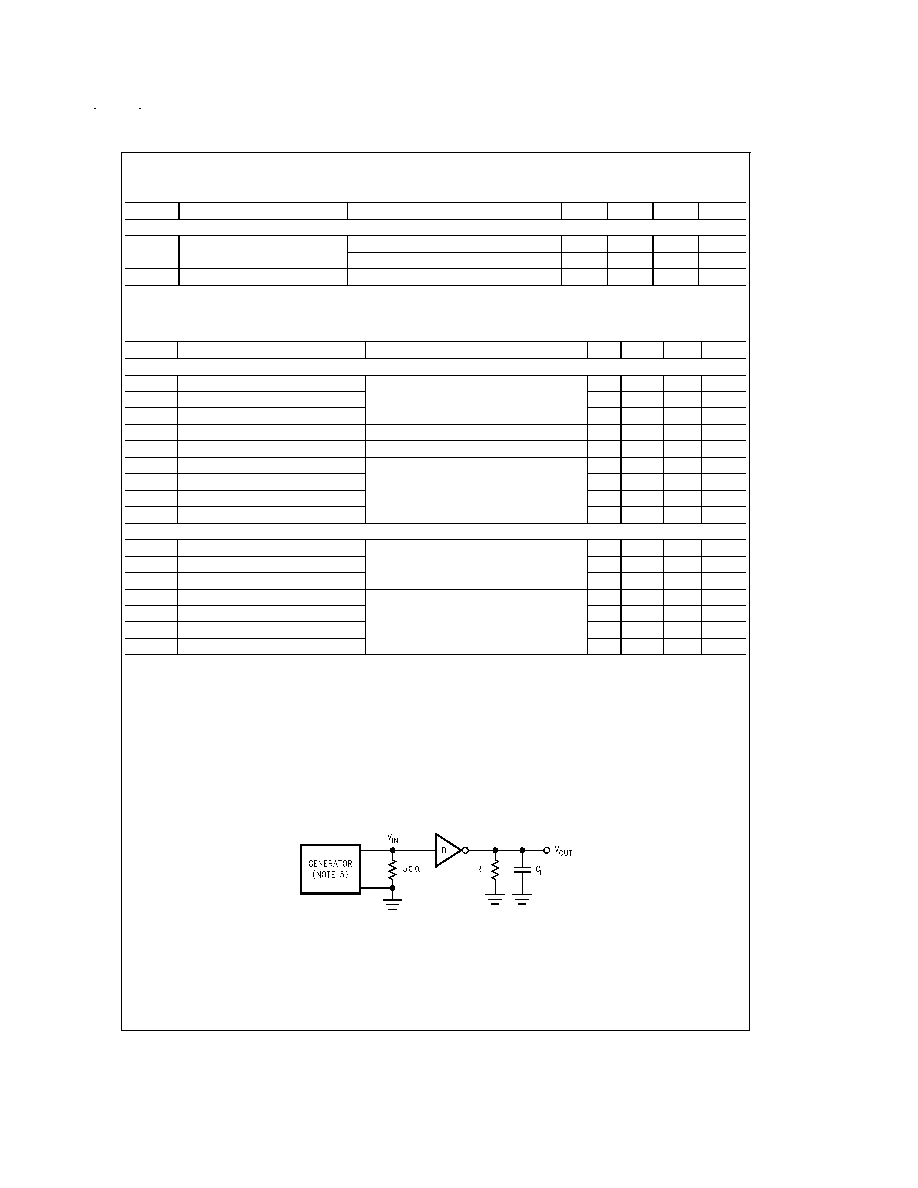
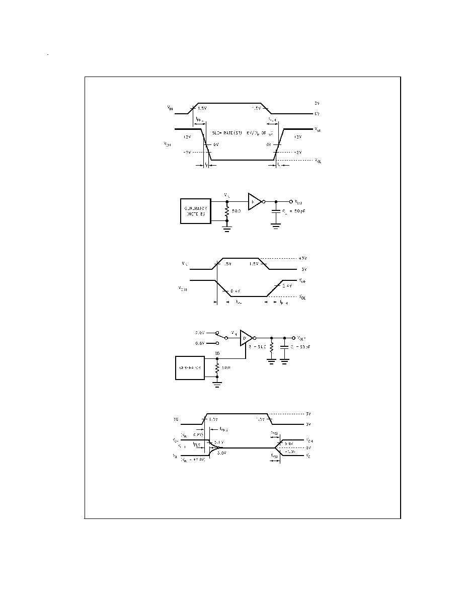
Parameter Measurement Information
DS011910-3
FIGURE 1. Driver Propagation Delay and Slew Rate Test Circuit
www.national.com
3
Parameter Measurement Information
(Continued)
DS011910-4
FIGURE 2. Driver Propagation Delay and Slew Rate Timing
DS011910-5
FIGURE 3. Receiver Propagation Delay Test Circuit
DS011910-6
FIGURE 4. Receiver Propagation Delay Timing
DS011910-7
FIGURE 5. Driver SHUTDOWN (SD) Delay Test Circuit
DS011910-8
FIGURE 6. Driver SHUTDOWN (SD) Delay Timing
www.national.com
4
Parameter Measurement Information
(Continued)
Pin Descriptions
V
CC
(Pin 3). Power supply pin for the device, +5V (
±
0.5V).
V+ (Pin 1). Positive supply for EIA/TIA-232-E drivers. Rec-
ommended external capacitor -- 0.1 µF (16V). This supply is
not intended to be loaded externally.
V- (Pin 25). Negative supply for EIA/TIA-232-E drivers. Rec-
ommended external capacitor -- 0.1 µF (16V). This supply is
not intended to be loaded externally.
C1+, C1- (Pins 2, 4). External capacitor connection pins.
C2+, C2- (Pins 28, 26). External capacitor connection pins.
SHUTDOWN (SD) (Pin 23). A High on the SHUTDOWN pin
will lower the total I
CC
current to less than 10 µA, providing a
low power state. In this mode receiver R5 remains active.
The SD pin should be driven or tied low (GND) to disable the
shutdown mode.
D
IN
1≠3 (Pins 7, 8, 9). Driver input pins.
D
OUT
1≠3 (Pins 22, 21, 20). Driver output pins conform to
EIA/TlA-232 -E levels.
R
IN
1≠5 (Pins 19, 18, 17, 16, 15). Receiver input pins accept
EIA/TIA-232-E input voltages (
±
25V). Receivers guarantees
hysteresis of TBD mV. Unused receiver input pins may be
left open. Internal input resistor (5 k
) pulls input LOW, pro-
viding a failsafe HIGH output.
R
OUT
1≠5 (Pins 10, 11, 12, 13, 14). Receiver output pins.
GND (Pins 5, 27). Ground Pins. Both pins must be con-
nected to external ground. These pins are not connected to-
gether on the chip.
Application Information
In a typical Data Terminal Equipment (DTE) to Data
Circuit-Terminating Equipment (DCE) 9-pin de-facto inter-
face implementation, 2 data lines and 6 control lines are re-
quired. The data lines are TXD and RXD and the control
lines are RTS, DTR, DSR, DCD, CTS and RI. The
DS14C535 is a 3 x 5 Driver/Receiver and offers a single chip
solution for the DTE interface as shown in
Figure 9 .
Ring Indicator (RI) is used to inform the DTE that an incom-
ing call is coming from a remote DCE. When the DS14C535
is in SHUTDOWN (SD) mode, receiver five (R5) remains ac-
tive and monitors RI circuit. This active receiver (R5) alerts
the DTE to switch the DS14C535 from SHUTDOWN to ac-
tive mode.
To achieve minimum power consumption, the DS14C535
can be in SHUTDOWN mode and only activated when com-
munications are needed.
DS011910-9
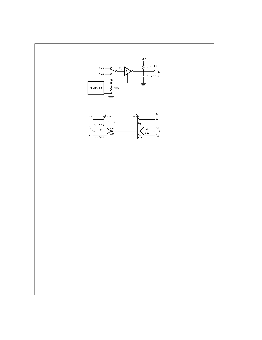
FIGURE 7. Receiver SHUTDOWN (SD) Delay Test Circuit
DS011910-10
FIGURE 8. Receiver SHUTDOWN (SD) Delay Timing
www.national.com
5