DS15MB200
Dual 1.5 Gbps 2:1/1:2 LVDS Mux/Buffer with
Pre-Emphasis
General Description
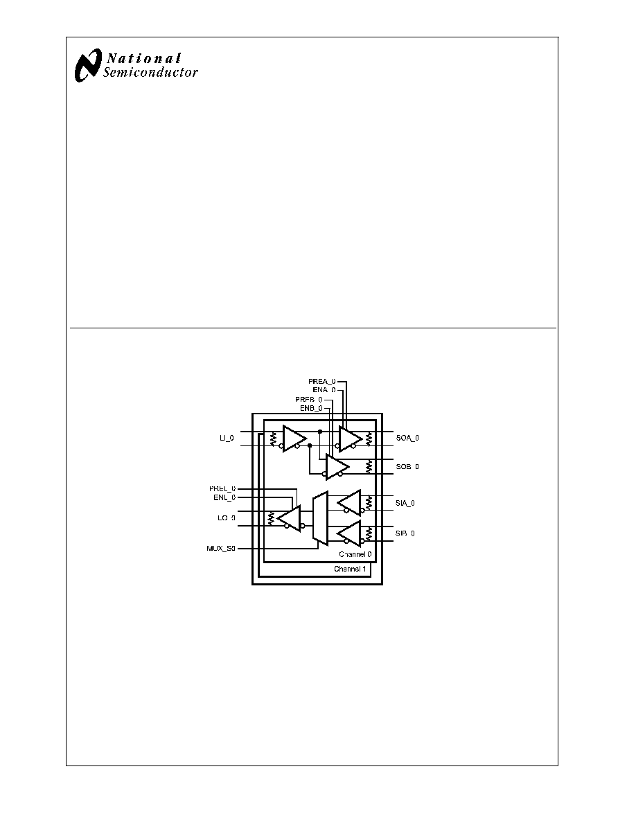
The DS15MB200 is a dual-port 2 to 1 multiplexer and 1 to 2
repeater/buffer. High-speed data paths and flow-through pi-
nout minimize internal device jitter and simplify board layout,
while pre-emphasis overcomes ISI jitter effects from lossy
backplanes and cables. The differential inputs and outputs
interface to LVDS or Bus LVDS signals such as those on
National's 10-, 16-, and 18- bit Bus LVDS SerDes, or to CML
or LVPECL signals.
The 3.3V supply, CMOS process, and robust I/O ensure high
performance at low power over the entire industrial -40 to
+85∞C temperature range.
Features
n
1.5 Gbps data rate per channel
n
Configurable off/on pre-emphasis drives lossy
backplanes and cables
n
LVDS/BLVDS/CML/LVPECL compatible inputs, LVDS
compatible outputs
n
Low output skew and jitter
n
On-chip 100
input and output termination
n
15 kV ESD protection on LVDS inputs/outputs
n
Hot plug Protection
n
Single 3.3V supply
n
Industrial -40 to +85∞C temperature range
n
48-pin LLP Package
Block Diagram
20157301
FIGURE 1. DS15MB200 Block Diagram
February 2006
DS15MB200
Dual
1.5
Gbps
2:1/1:2
L
VDS
Mux/Buffer
with
Pre-Emphasis
© 2006 National Semiconductor Corporation
DS201573
www.national.com
Pin Descriptions
Pin
Name
LLP Pin
Number
I/O, Type
Description
SWITCH SIDE DIFFERENTIAL INPUTS
SIA_0+
SIA_0-
30
29
I, LVDS
Switch A-side Channel 0 inverting and non-inverting differential inputs. LVDS, Bus LVDS,
CML, or LVPECL compatible.
SIA_1+
SIA_1-
19
20
I, LVDS
Switch A-side Channel 1 inverting and non-inverting differential inputs. LVDS, Bus LVDS,
CML, or LVPECL compatible.
SIB_0+
SIB_0-
28
27
I, LVDS
Switch B-side Channel 0 inverting and non-inverting differential inputs. LVDS, Bus LVDS,
CML, or LVPECL compatible.
SIB_1+
SIB_1-
21
22
I, LVDS
Switch B-side Channel 1 inverting and non-inverting differential inputs. LVDS, Bus LVDS,
CML, or LVPECL compatible.
LINE SIDE DIFFERENTIAL INPUTS
LI_0+
LI_0-
40
39
I, LVDS
Line-side Channel 0 inverting and non-inverting differential inputs. LVDS, Bus LVDS, CML, or
LVPECL compatible.
LI_1+
LI_1-
9
10
I, LVDS
Line-side Channel 1 inverting and non-inverting differential inputs. LVDS, Bus LVDS, CML, or
LVPECL compatible.
SWITCH SIDE DIFFERENTIAL OUTPUTS
SOA_0+
SOA_0-
34
33
O, LVDS
Switch A-side Channel 0 inverting and non-inverting differential outputs. LVDS compatible
(Notes 1, 3).
SOA_1+
SOA_1-
15
16
O, LVDS
Switch A-side Channel 1 inverting and non-inverting differential outputs. LVDS compatible
(Notes 1, 3).
SOB_0+
SOB_0-
32
31
O, LVDS
Switch B-side Channel 0 inverting and non-inverting differential outputs. LVDS compatible
(Notes 1, 3).
SOB_1+
SOB_1-
17
18
O, LVDS
Switch B-side Channel 1 inverting and non-inverting differential outputs. LVDS compatible
(Notes 1, 3).
LINE SIDE DIFFERENTIAL OUTPUTS
LO_0+
LO_0-
42
41
O, LVDS
Line-side Channel 0 inverting and non-inverting differential outputs. LVDS compatible (Notes
1, 3).
LO_1+
LO_1-
7
8
O, LVDS
Line-side Channel 1 inverting and non-inverting differential outputs. LVDS compatible (Notes
1, 3).
DIGITAL CONTROL INTERFACE
MUX_S0
MUX_S1
38
11
I, LVTTL
Mux Select Control Inputs (per channel) to select which Switch-side input, A or B, is passed
through to the Line-side.
PREA_0
PREA_1
PREB_0
PREB_1
26
23
25
24
I, LVTTL
Output pre-emphasis control for Switch-side outputs. Each output driver on the Switch A-side
and B-side has a separate pin to control the pre-emphasis on or off.
PREL_0
PREL_1
44
5
I, LVTTL
Output pre-emphasis control for Line-side outputs. Each output driver on the Line A-side and
B-side has a separate pin to control the pre-emphasis on or off.
ENA_0
ENA_1
ENB_0
ENB_1
36
13
35
14
I, LVTTL
Output Enable Control for Switch A-side and B-side outputs. Each output driver on the A-side
and B-side has a separate enable pin.
ENL_0
ENL_1
45
4
I, LVTTL
Output Enable Control for The Line-side outputs. Each output driver on the Line-side has a
separate enable pin.
DS15MB200
www.national.com
2
Pin Descriptions
(Continued)
Pin
Name
LLP Pin
Number
I/O, Type
Description
POWER
V
DD
2, 6, 12,
37, 43,
46, 48
I, Power
V
DD
= 3.3V
±
0.3V.
GND
3, 47
(Note 2)
I, Power
Ground reference for LVDS and CMOS circuitry.
For the LLP package, the DAP is used as the primary GND connection to the device. The
DAP is the exposed metal contact at the bottom of the LLP-48 package. It should be
connected to the ground plane with at least 4 vias for optimal AC and thermal performance.
Note 1: For interfacing LVDS outputs to CML or LVPECL compatible inputs, refer to the applications section of this datasheet (planned).
Note 2: Note that the DAP on the backside of the LLP package is the primary GND connection for the device when using the LLP package.
Note 3: The LVDS outputs do not support a multidrop (BLVDS) environment. The LVDS output characteristics of the DS15MB200 device have been optimized for
point-to-point backplane and cable applications.
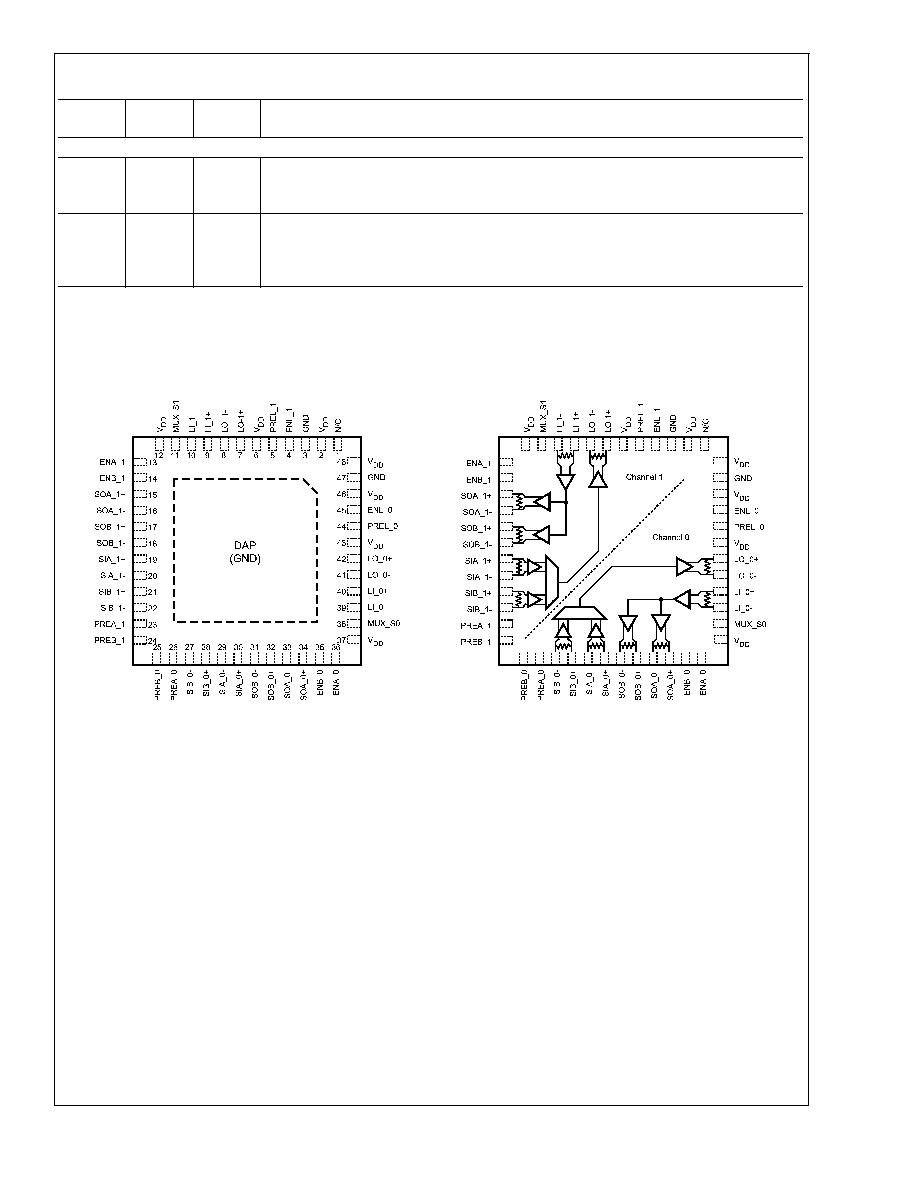
Connection Diagrams
20157302
LLP Top View
DAP = GND
20157303
Directional Signal Paths Top View
(Refer to pin names for signal polarity)
DS15MB200
www.national.com
3
Output Characteristics
The output characteristics of the DS15MB200 have been
optimized for point-to-point backplane and cable applica-
tions, and are not intended for multipoint or multidrop signal-
ing.
A 100
output (source) termination resistor is incorporated
in the device to eliminate the need for an external resistor,
providing excellent drive characteristics by locating the
source termination as close to the output as physically pos-
sible.
Pre-Emphasis Controls
The pre-emphasis is used to compensate for long or lossy
transmission media. Separate pins are provided for each
output to minimize power consumption. Pre-emphasis is
programmable to be off or on per the Pre-emphasis Control
Table.
PREx_n (Note 4)
Output Pre-emphasis
0
0%
1
100%
Note 4: Applies to PREA_0, PREA_1, PREB_0, PREB_1, PREL_0,
PREL_1
Multiplexer Truth Table
(Note 5)
Data Inputs
Control Inputs
Output
SIA_0
SIB_0
MUX_S0
ENL_0
LO_0
X
valid
0
1
SIB_0
valid
X
1
1
SIA_0
X
X
X
0
Z
X = Don't Care
Z = High Impedance (TRI-STATE)
Repeater/Buffer Truth Table
(Note 5)
Data
Input
Control Inputs
Outputs
LI_0
ENA_0
ENB_0
SOA_0
SOB_0
X
0
0
Z
Z
valid
0
1
Z
LI_0
valid
1
0
LI_0
Z
valid
1
1
LI_0
LI_0
X = Don't Care
Z = High Impedance (TRI-STATE)
Note 5: Same functionality for channel 1
DS15MB200
www.national.com
4
Absolute Maximum Ratings
(Note 6)
Supply Voltage (V
DD
)
-0.3V to +4.0V
CMOS Input Voltage
-0.3V to (V
DD
+0.3V)
LVDS Receiver Input Voltage
-0.3V to (V
DD
+0.3V)
LVDS Driver Output Voltage
-0.3V to (V
DD
+0.3V)
LVDS Output Short Circuit
Current
+40 mA
Junction Temperature
+150∞C
Storage Temperature
-65∞C to +150∞C
Lead Temperature (Solder, 4sec)
260∞C
Max Pkg Power Capacity
@
25∞C
5.2W
Thermal Resistance (
JA
)
24∞C/W
Package Derating above +25∞C
41.7mW/∞C
ESD Last Passing Voltage
HBM, 1.5k
, 100pF
8kV
LVDS pins to GND only
15kV
EIAJ, 0
, 200pF
250V
CDM
1000V
Recommended Operating
Conditions
Supply Voltage (V
CC
)
3.0V to 3.6V
Input Voltage (V
I
) (Note 7)
0V to V
CC
Output Voltage (V
O
)
0V to V
CC
Operating Temperature (T
A
)
Industrial
-40∞C to +85∞C
Note 6: Absolute maximum ratings are those values beyond which damage
to the device may occur. The databook specifications should be met, without
exception, to ensure that the system design is reliable over its power supply,
temperature, and output/input loading variables. National does not recom-
mend operation of products outside of recommended operation conditions.
Note 7: V
ID
max
<
2.4V
Electrical Characteristics
Over recommended operating supply and temperature ranges unless other specified.
Symbol
Parameter
Conditions
Min
Typ
(Note 8)
Max
Units
LVTTL DC SPECIFICATIONS (MUX_Sn, PREA_n, PREB_n, PREL_n, ENA_n, ENB_n, ENL_n)
V
IH
High Level Input Voltage
2.0
V
DD
V
V
IL
Low Level Input Voltage
GND
0.8
V
I
IH
High Level Input Current
V
IN
= V
DD
= V
DDMAX
-10
+10
µA
I
IHR
High Level Input Current
PREA_n, PREB_n, PREL_n
40
200
µA
I
IL
Low Level Input Current
V
IN
= V
SS
, V
DD
= V
DDMAX
-10
+10
µA
C
IN1
Input Capacitance
Any Digital Input Pin to V
SS
2.0
pF
C
OUT1
Output Capacitance
Any Digital Output Pin to V
SS
4.0
pF
V
CL
Input Clamp Voltage
I
CL
= -18 mA
-1.5
-0.8
V
LVDS INPUT DC SPECIFICATIONS (SIA
±
, SIB
±
, LI
±
)
V
TH
Differential Input High Threshold
(Note 9)
V
CM
= 0.8V or 1.2V or 3.55V,
V
DD
= 3.6V
0
100
mV
V
TL
Differential Input Low Threshold
(Note 9)
V
CM
= 0.8V or 1.2V or 3.55V,
V
DD
= 3.6V
-100
0
mV
V
ID
Differential Input Voltage
V
CM
= 0.8V to 3.55V, V
DD
= 3.6V
100
2400
mV
V
CMR
Common Mode Voltage Range
V
ID
= 150 mV, V
DD
= 3.6V
0.05
3.55
V
C
IN2
Input Capacitance
IN+ or IN- to V
SS
2.0
pF
I
IN
Input Current
V
IN
= 3.6V, V
DD
= V
DDMAX
or 0V
-15
+15
µA
V
IN
= 0V, V
DD
= V
DDMAX
or 0V
-15
+15
µA
LVDS OUTPUT DC SPECIFICATIONS (SOA_n
±
, SOB_n
±
, LO_n
±
)
V
OD
Differential Output Voltage,
0% Pre-emphasis (Note 9)
R
L
is the internal 100
between OUT+
and OUT-
250
360
500
mV
V
OD
Change in V
OD
between
Complementary States
-35
35
mV
V
OS
Offset Voltage (Note 10)
1.05
1.22
1.475
V
V
OS
Change in V
OS
between
Complementary States
-35
35
mV
I
OS
Output Short Circuit Current
OUT+ or OUT- Short to GND
-21
-40
mA
C
OUT2
Output Capacitance
OUT+ or OUT- to GND when
TRI-STATE
4.0
pF
DS15MB200
www.national.com
5