 | –≠–ª–µ–∫—Ç—Ä–æ–Ω–Ω—ã–π –∫–æ–º–ø–æ–Ω–µ–Ω—Ç: DS25C400 | –°–∫–∞—á–∞—Ç—å:  PDF PDF  ZIP ZIP |
DS25C400
Quad 2.5 Gbps Serializer/Deserializer
General Description
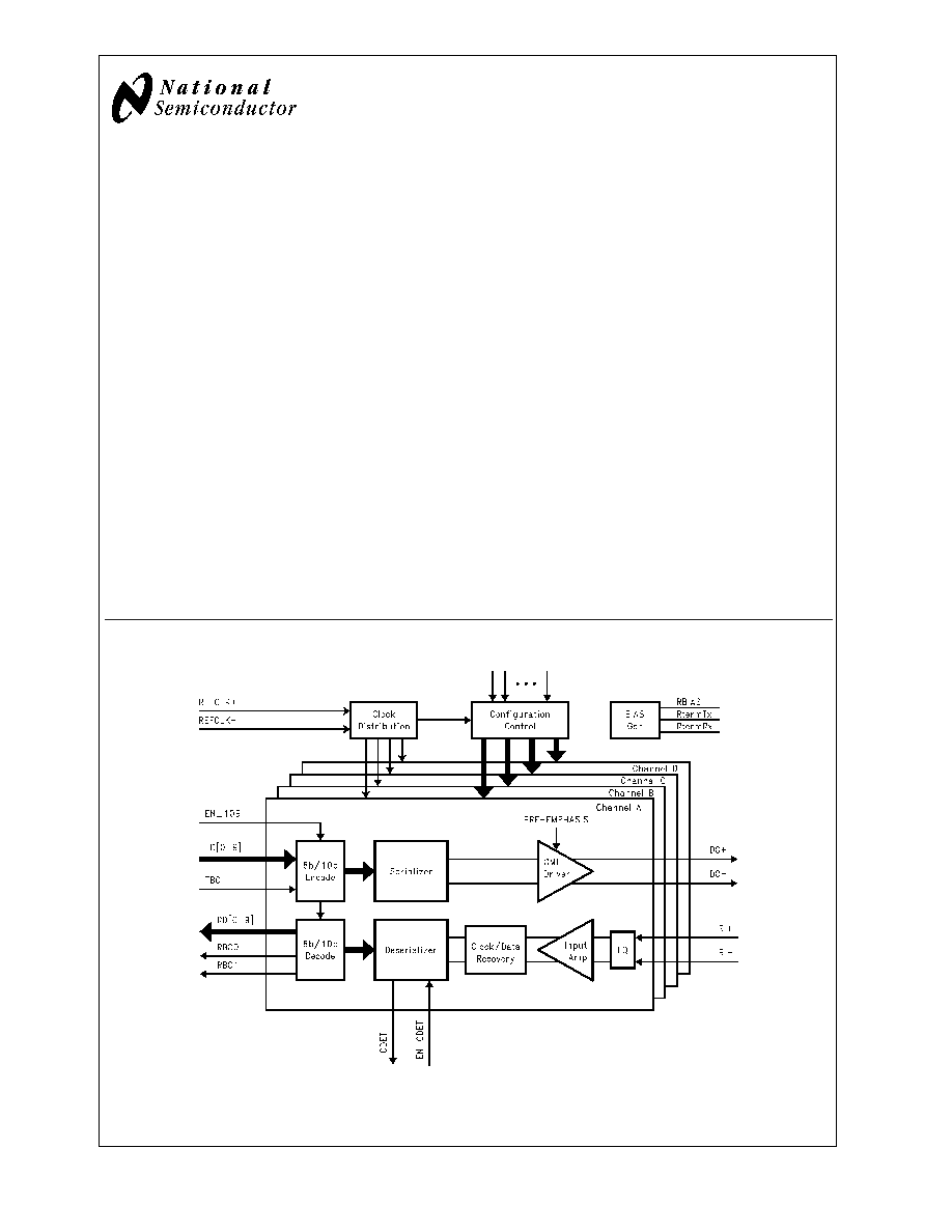
The DS25C400 is a four-channel serializer/deserializer
(SERDES) for high-speed serial data transmission over con-
trolled impedance transmission media such as a printed
circuit board backplane or twin-axial cable. It is capable of
transmitting and receiving serial data of 2.125 - 2.5 Gbps or
1.0625 - 1.25 Gbps per channel.
Each transmit section of the DS25C400 contains a low-jitter
clock synthesizer, an 8-bit or 10-bit parallel to serial con-
verter with built in 8b/10b encoder, and a CML output driver
with selectable pre-emphasis optimized for backplane appli-
cations. Its receive section contains an input limiting ampli-
fier with on-chip terminations and selectable equalization
levels, a clock/data recovery PLL, a comma detector and a
serial to parallel converter with built-in 8b/10b decoder.
The DS25C400 has built-in local loopback test mode,
pseudo-random pattern generator and error detector to sup-
port self-testing.
The DS25C400 requires no external components for its
clock synthesizers and clock recovery PLL's. Three external
resistors are needed to set the proper bias currents and
compensate for process variations to achieve tight tolerance
on-chip terminations.
Features
n
Quad Serializer/Deserializer
n
Data rate per channel: 2.125 - 2.5 Gbps or 1.0625 -
1.25 Gbps
n
Supports 106.25 - 125 MHz differential reference input
clock
n
Low jitter clock synthesizers for clock distribution
n
8-bit or 10-bit parallel I/O Interface conforms to
SSTL_18 Class 1 (also interfaces to 1.8V HSTL or 1.8V
LVCMOS)
n
On-chip 8b/10b encoder and decoder
n
High speed serial CML drivers
n
High speed serial CML on-chip terminations
n
Selectable pre-emphasis and equalization
n
On-chip Comma Detect for character alignment
n
On-chip local loopback test mode
n
On-chip pattern generator and error checker to support
BIST
n
Hot plug protection
n
Low power, 420 mW (typ) per channel
n
324-ball TE-PBGA package
n
Operating temperature -40∞C to +85∞C
General Function Diagram
20030101
PRELIMINARY
September 2002
DS25C400
Quad
2.5
Gbps
Serializer/Deserializer
© 2002 National Semiconductor Corporation
DS200301
www.national.com
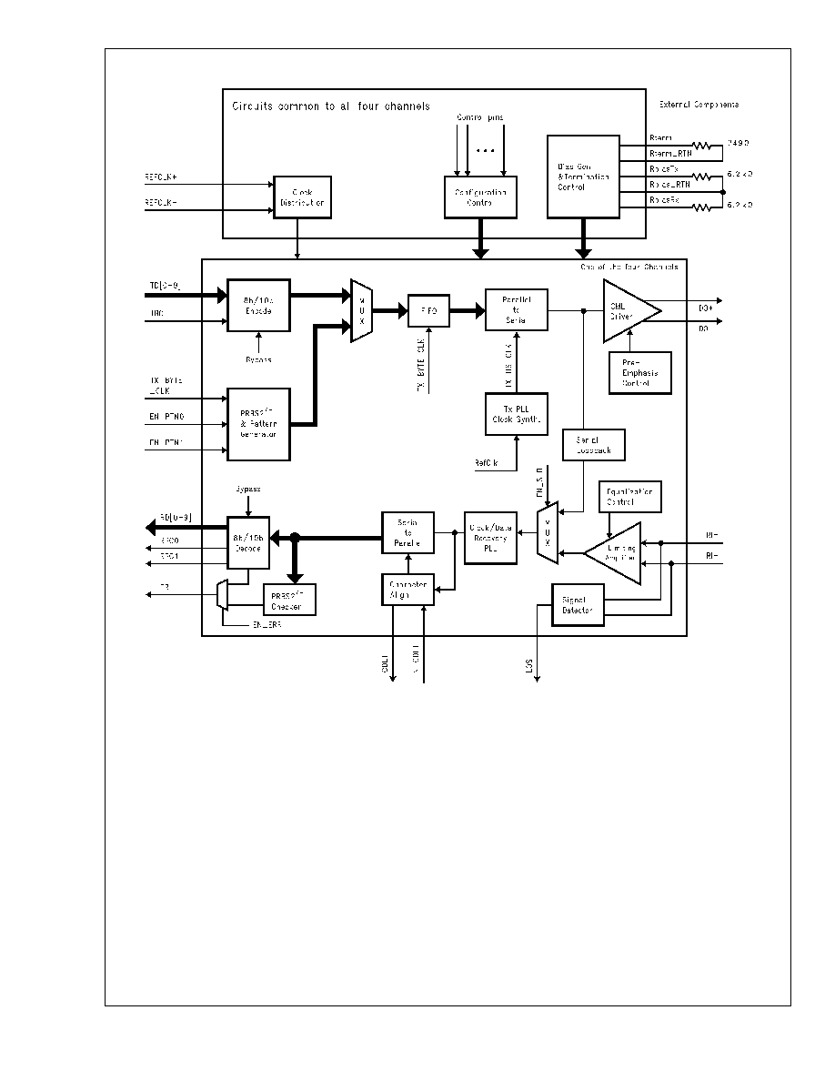
Functional Block Diagram
20030102
DS25C400
www.national.com
2
Absolute Maximum Ratings
(Note 1)
If Military/Aerospace specified devices are required,
please contact the National Semiconductor Sales Office/
Distributors for availability and specifications.
Supply Voltage
(V
DDQ
, DV
DD
)
-0.3V to +2.3V
Supply Voltage
(V
DDIO
, V
DDHS
, V
DDB
)
-0.3V to +3.0V
SSTL Input Voltage
-0.3V to (V
DDQ
+ 0.3V)
LVCMOS Input Voltage
-0.3V to (DV
DD
+ 0.3V)
LVCMOS Output Voltage
-0.3V to (DV
DD
+ 0.3V)
CML Receiver Input Voltage
-0.3V to (V
DDHS
+ 0.3V)
CML Driver Output Voltage
-0.3V to (V
DDHS
+ 0.3V)
Junction Temperature
+125∞C
Storage Temperature
-65∞C to +150∞C
Lead Temperature
Soldering, 4 Seconds
+260∞C
Maximum Package Power Dissipation at 25∞C
DS25C400TUT
5.68 W
Derating above 25∞C
45.45 mW/∞C
Thermal Resistance,
JA
22 ∞C/W
Junction-to-case Conductive
Thermal Resistance,
JC
6.5 ∞C/W
ESD Rating
HBM, 1.5 k
, 100 pF
EIAJ, 0
, 200 pF
>
2 kV
>
200 V
Recommended Operating
Conditions
Min
Typ
Max
Unit
Supply Voltage
V
DDQ
and DV
DD
to DGND
1.7
1.8
1.9
V
V
DDIO
, V
DDHS
and V
DDB
to DGND or AGND
2.35
2.5
2.65
V
Temperature
-40
25
85
∞C
Supply Noise Amplitude
<
100mV
P-P
Supply Noise Frequency
<
1
MHz
Electrical Characteristics
Over recommended operating supply and temperature ranges unless otherwise specified.
Symbol
Parameter
Conditions
Min
Typ
(Note 2)
Max
Units
SSTL_18 DC SPECIFICATIONS -- Parallel I/O, Class I
V
REF
Reference Voltage
0.83
0.90
0.97
V
V
TT
Termination Voltage
V
REF
-
0.04
V
REF
V
REF
+
0.04
V
V
IH
(dc)
High Level Input Voltage
V
REF
+0.125
V
DDQ
+0.300
V
V
IH
(ac)
AC Input Logic High
V
REF
+0.250
V
V
IL
(dc)
Low Level Input Voltage
-0.300
V
REF
-0.125
V
V
IL
(ac)
AC Input Logic Low
V
REF
-0.250
V
I
IH
High Level Input Current
V
IN
= V
DDQ
= 1.9 V
-10
+50
µA
I
IL
Low Level Input Current
V
IN
= GND, V
DDQ
= 1.9 V
-10
+10
µA
V
OH
(dc)
High Level Output Voltage
I
OH
= -6.3 mA, Unterminated,
C
L
= 8pF
V
DDQ
-0.400
V
Terminated, R = 50
to V
TT
V
DDQ
-0.550
V
V
OL
(dc)
Low Level Output Voltage
I
OL
= 6.3 mA, Unterminated,
C
L
= 8pF
0.400
V
Terminated, R = 50
to V
TT
0.550
V
LVCMOS DC SPECIFICATIONS -- Control Pins EIA/JESD8-7 Compliant
V
IH
High Level Input Voltage
0.65
*
DV
DD
DV
DD
V
V
IL
Low Level Input Voltage
0
0.35
*
DV
DD
V
DS25C400
www.national.com
3
Electrical Characteristics
Over recommended operating supply and temperature ranges unless otherwise
specified. (Continued)
Symbol
Parameter
Conditions
Min
Typ
(Note 2)
Max
Units
LVCMOS DC SPECIFICATIONS -- Control Pins EIA/JESD8-7 Compliant
I
IH
High Level Input Current
V
IN
= DV
DD
= 1.9 V
(input and pull-low)
0.1
mA
I
IH
High Level Input Current
V
IN
= DV
DD
= 1.9 V
(input with pull-high)
-10
+10
µA
I
IL
Low Level Input Current
V
IN
= GND, DV
DD
= 1.9 V
(input with pull-low)
-10
+10
µA
I
IL
Low Level Input Current
V
IN
= GND, DV
DD
= 1.9 V
(input with pull-high)
-0.1
mA
V
OH
High Level Output Voltage
I
OH
= -2 mA
DV
DD
-0.45
V
V
OL
Low Level Output Voltage
I
OL
= 2 mA
0.45
V
SUPPLY CURRENT
I
DD
Total Supply Current
K28.5 pattern at 2.5 Gbps with no
pre-emphasis. SSTL outputs no load
termination resistors, Tx high speed
serial outputs driving 100
differential, no high speed Rx input
data.
V
DDHS
+ V
DDIO
+ V
DDB
572
600
mA
DV
DD
+ V
DDQ
130
136.5
mA
P
D
Total Power Consumption
K28.5 pattern at 2.5 Gbps with no
pre-emphasis. SSTL outputs no load
termination resistors, Tx high speed
serial outputs driving 100
differential, no high speed Rx input
data.
SERDES and SSTL I/O
1708
1940
mW
RECOMMENDED INPUT REFERENCE CLOCK (REFCLK
±
) AC coupled differential signal
VIDS
RCLK
Differential Input Voltage
Figure 1
Terminated by 50
parallel
termination
600
1500
mV
p-p
V
ICM
Common Mode Voltage
Terminated by 50
Parallel
Termination
1.0
V
DDHS
-0.5
V
R
REFCLK
Input Termination to GND
Equivalent Parallel Input Termination
at REFCLK+ or REFCLK- to GND
100
f
REF
REFCLK Frequency Range
106.25
125
MHz
df
REF
REFCLK Frequency Variation
Variation from Nominal Frequency
-100
+100
ppm
t
REF-DC
REFCLK Duty Cycle (Note 3)
Between 50% of the differential
voltage across REFCLK+ and
REFCLK-
40
50
60
%
t
REF-RJ
REFCLK Input
Random (rms) Jitter
3
5
ps
t
REF-RJ
REFCLK Input
Peak-to-Peak Jitter
25
40
ps
t
REF-X
REFCLK Transition Time
Figure 1
Transition time between 20% and
80% of the differential voltage across
REFCLK+ and REFCLK-
0.2
1
ns
DS25C400
www.national.com
4
Electrical Characteristics
Over recommended operating supply and temperature ranges unless otherwise
specified. (Continued)
Symbol
Parameter
Conditions
Min
Typ
(Note 2)
Max
Units
SERIALIZER
DR
DO
Transmit Data Rate
Data Rate at DO
±
High Data Rate Mode (EN_HDR = 1)
2.125
2.5
Gbps
Low Data Rate Mode (EN_HDR = 0)
1.0625
1.25
Gbps
V
ODS
Output Differential Voltage
Swing (DO+ - DO-) WITHOUT
Pre-emphasis
DO+, DO- are terminated by external
50
to V
DDHS
PSEL1 = 0, PSEL0 = 0
850
1065
1280
mV
p-p
Output Differential Voltage
Swing (DO+ - DO-) WITH
Pre-emphasis
DO+, DO- are terminated by external
50
to V
DDHS
PSEL1 = 0, PSEL0 = 1
TBD
1330
TBD
mV
p-p
PSEL1 = 1, PSEL0 = 0
TBD
1600
TBD
PSEL1 = 1, PSEL0 = 1
TBD
1850
TBD
V
CM
Output Common Mode Offset
Voltage WITHOUT
Pre-emphasis
DO+, DO- are terminated by external
50
to V
DDHS
PSEL1 = 0, PSEL0 = 0
-10%
V
DDHS
-0.3
+10%
V
Output Common Mode Offset
Voltage WITH Pre-emphasis
DO+, DO- are terminated by external
50
to V
DDHS
PSEL1 = 0, PSEL0 = 1
-10%
V
DDHS
-0.37
+10%
V
PSEL1 = 1, PSEL0 = 0
V
DDHS
-0.43
PSEL1 = 1, PSEL0 = 1
V
DDHS
-0.50
R
DO
Output Resistance
On-chip termination DO+ or DO- to
V
DDHS
, RTERM = 249
45
50
55
C
DO
Capacitance to GND
DO+ or DO- to GND
1
pF
t
DO-X
Serial Data Output Transition
Time
Measured between 20% and 80% of
V
ODS
100
120
160
ps
JIT
DO-DJ
Serial Data Output
Deterministic Jitter
(Peak-to-Peak),
(Notes 4, 5)
Output K28.5 at 2.5 Gbps
0.1
0.13
UI
JIT
DO-RJ
Serial Data Output Random
Jitter (Peak-to-Peak),
(Notes 4, 5)
Output D21.5 at 2.5 Gbps
0.13
0.15
UI
JIT
DO-TJ
Serial Data Output Total Jitter,
(Notes 4, 5)
Output K28.5 pattern at 2.5 Gbps at
BER of 10
-12
0.2
0.25
UI
t
LAT-TX
Transmit Latency Figure 2
Transmit K28.5 from TD[0≠9] to DO
±
at 2.5 Gbps, EN_10B = 1
35
48
Bits
Transmit K28.5 from TD[0≠9] to DO
±
at 2.5 Gbps, EN_10B = 0
45
58
Bits
t
DO-LOCK
Lock Time
Time to achieve frequency lock to
REFCLK. Output K28.5 at 2.5 Gbps.
0.5
ms
DESERIALIZER
DR
RI
Receive Data Rate
High Data Rate (EN_HDR = 1)
2.125
2.5
Gbps
Low Data Rate (EN_HDR = 0)
1.0625
1.25
Gbps
VIDS
RI
Differential Input Voltage
RI+ ≠ RI-
200
1500
mV
p-p
R
RI
Input Termination to V
DDHS
On-chip termination RI+ to RI- to
V
DDHS
EN_RAC = 0, RTERM = 249
:
45
50
55
DS25C400
www.national.com
5