DS26LV32AT
3V Enhanced CMOS Quad Differential Line Receiver
General Description
The DS26LV32A is a high speed quad differential CMOS
receiver that meets the requirements of both TIA/EIA-422-B
and ITU-T V.11. The CMOS DS26LV32AT features typical
low static I
CC
of 9 mA which makes it ideal for battery
powered and power conscious applications. The TRI-
STATE
Æ
enables, EN and EN*, allow the device to be active
High or active Low. The enables are common to all four
receivers.
The receiver output (RO) is guaranteed to be High when the
inputs are left open. The receiver can detect signals as low
as
±
200 mV over the common mode range of
±
10V. The
receiver outputs (RO) are compatible with TTL and LVCMOS
levels.
Features
n
Low Power CMOS design (30 mW typical)
n
Interoperable with existing 5V RS-422 networks
n
Industrial and Military Temperature Range
n
Conforms to TIA/EIA-422-B (RS-422) and ITU-T V.11
Recommendation
n
3.3V Operation
n
±
7V Common Mode Range
@
V
ID
= 3V
n
±
10V Common Mode Range
@
V
ID
= 0.2V
n
Receiver OPEN input failsafe feature
n
Guaranteed AC Parameter:
Maximum Receiver Skew:
4 ns
Maximum Transition Time:
10 ns
n
Pin compatible with DS26C32AT
n
32 MHz Toggle Frequency
n
>
6.5k ESD Tolerance (HBM)
n
Available in SOIC and Cerpack Packaging
n
Standard Microcircuit Drawing (SMD) 5962-98585
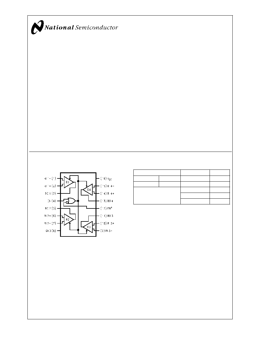
Connection Diagram
Dual-In-Line Package
01290801
Top View
Order Number DS26LV32ATM or DS26LV32AW
See NS Package Number M16A or W16A
Truth Table
Enables
Inputs
Output
EN
EN*
RI+≠RI-
RO
L
H
X
Z
All Other
V
ID
+0.2V
H
Combinations of
V
ID
-0.2V
L
Enable Inputs
Open
H
Open, not terminated
L = Logic Low
H = Logic High
X = Irrelevant
Z = TRI-STATE
TRI-STATE
Æ
is a registered trademark of National Semiconductor Corporation.
March 2000
DS26L
V32A
T
3
V
Enhanced
CMOS
Quad
Differential
Line
Receiver
© 2002 National Semiconductor Corporation
DS012908
www.national.com

Absolute Maximum Ratings
(Note 1)
If Military/Aerospace specified devices are required,
please contact the National Semiconductor Sales Office/
Distributors for availability and specifications.
Supply Voltage (V
CC
)
-0.5V to +7V
Enable Input Voltage (EN, EN*)
-0.5V to V
CC
+0.5V
Receiver Input Voltage (V
ID
: RI+,
RI-)
±
14V
Receiver Input Voltage
(VCM: RI+, RI-)
±
14V
Receiver Output Voltage (RO)
-0.5V to V
CC
+0.5V
Receiver Output Current (RO)
±
25 mA Maximum
Maximum Package Power Dissipation
@
+25∞C
M Package
1190 mW
W Package
1087 mW
Derate M Package 9.8 mW/∞C above +25∞C
Derate W Package 7.3 mW/∞C above +25∞C
Storage Temperature Range
-65∞C to +150∞C
Lead Temperature Range Soldering
(4 Sec.)
+260∞C
ESD Ratings (HBM, 1.5 k
, 100 pF)
Receiver Inputs and Enables
6.5 kV
Other Pins
2 kV
Recommended Operating
Conditions
Min
Typ
Max
Units
Supply Voltage (V
CC
)
3.0
3.3
3.6
V
Operating Free Air Temperature Range (T
A
)
DS26LV32AT
-40
+25
+85
∞C
DS26LV32AW
-55
+25
+125
∞C
Electrical Characteristics
(Notes 2, 3)
Over Supply Voltage and Operating Temperature ranges, unless otherwise specified.
Symbol
Parameter
Conditions
Pin
Min
Typ
Max
Units
V
TH
Differential Input Threshold
V
OUT
= V
OH
or
V
OL
V
CM
= -7V to
+7V, T
A
= -40∞C
to +85∞C
RI+,
RI-
-200
±
17.5
+200
mV
V
CM
= -0.5V to
+5.5V, T
A
=
-55∞C to +125∞C
(Note 9)
-200
+200
mV
V
HY
Hysteresis
V
CM
= 1.5V
35
mV
V
IH
Minimum High Level
EN,
EN*
2.0
V
Input Voltage
V
IL
Maximum Low Level
0.8
V
Input Voltage
R
IN
Input Resistance
V
IN
= -7V, +7V, T
A
= -40∞C to
+85∞C (Other Input = GND)
RI+,
RI-
5.0
8.5
k
V
IN
= -0.5V, +5.5V, T
A
= -55∞C to
+125∞C (Other Input = GND) (Note
9)
5.0
k
I
IN
Input Current
V
IN
= +10V
T
A
= -40∞C to
+85∞C
0
1.1
1.8
mA
(Other Input = 0V,
V
IN
= +3V
0
0.27
mA
Power On, or
V
IN
= 0.5V
-0.02
mA
V
CC
= 0V)
V
IN
= -3V
0
-0.43
mA
V
IN
= -10V
0
-1.26
-2.2
mA
V
IN
= -0.5V
T
A
= -55∞C to
+125∞C (Note 9)
0
-1.8
mA
V
IN
= 5.5V
0
1.8
mA
I
EN
Input Current
V
IN
= 0V to V
CC
EN,
EN*
±
1
µA
DS26L
V32A
T
www.national.com
2
Electrical Characteristics
(Notes 2, 3) (Continued)
Over Supply Voltage and Operating Temperature ranges, unless otherwise specified.
Symbol
Parameter
Conditions
Pin
Min
Typ
Max
Units
V
OH
High Level Output Voltage
I
OH
= -6 mA, V
ID
= +1V
RO
2.4
3
V
I
OH
= -6 mA, V
ID
= OPEN
V
OH
High Level Output Voltage
I
OH
= -100 µA, V
ID
= +1V
V
CC
-0.1
V
I
OH
= - 100 µA, V
ID
= OPEN
V
OL
Low Level Output Voltage
I
OL
= +6 mA, V
ID
= -1V
0.13
0.5
V
I
OZ
Output TRI-STATE Leakage
V
OUT
= V
CC
or GND
±
50
µA
Current
EN = V
IL
, EN* = V
IH
I
SC
Output Short Circuit Current
V
O
= 0V, V
ID
|200 mV| (Note 4)
-10
-35
-70
mA
I
CC
Power Supply Current
No Load, All
RI+, R1- =
OPEN, EN, EN*
= V
CC
or GND
T
A
= -40∞C to
+85∞C
V
CC
9
15
mA
T
A
= -55∞C to
+125∞C
20
mA
Switching Characteristics - Industrial
(Notes 3, 7, 10, 11)
Over Supply Voltage and -40∞C to +85∞C Operating Temperature range, unless otherwise specified.
Symbol
Parameter
Conditions
Min
Typ
Max
Units
t
PHL
Propagation Delay
C
L
= 15 pF, V
CM
= 1.5V (
Figures
1, 2 )
6
17.5
35
ns
High to Low
t
PLH
Propagation Delay
6
17.8
35
ns
Low to High
t
r
Rise Time (20% to 80%)
4.1
10
ns
t
f
Fall Time (80% to 20%)
3.3
10
ns
t
PHZ
Disable Time
C
L
= 50 pF, V
CM
= 1.5V (
Figures
3, 4 )
40
ns
t
PLZ
Disable Time
40
ns
t
PZH
Enable Time
40
ns
t
PZL
Enable Time
40
ns
t
SK1
Skew, |t
PHL
- t
PLH
| (Note 5)
C
L
= 15 pF, V
CM
= 1.5V
0.3
4
ns
t
SK2
Skew, Pin to Pin (Note 6)
0.6
4
ns
t
SK3
Skew, Part to Part (Note 7)
7
17
ns
f
MAX
Maximum Operating
Frequency (Note 8)
C
L
= 15 pF, V
CM
= 1.5V
32
MHz
DS26L
V32A
T
www.national.com
3
Switching Characteristics - Military
(Notes 10, 11)
Over Supply Voltage and -55∞C to +125∞C Operating Temperature range, unless otherwise specified.
Symbol
Parameter
Conditions
Min
Max
Units
t
PHL
Propagation Delay
C
L
= 50 pF, V
CM
= 1.5V (
Figures
1, 2 )
6
45
ns
High to Low
t
PLH
Propagation Delay
6
45
ns
Low to High
t
PHZ
Disable Time
C
L
= 50 pF, V
CM
= 1.5V (
Figures
3, 4 )
50
ns
t
PLZ
Disable Time
50
ns
t
PZH
Enable Time
50
ns
t
PZL
Enable Time
50
ns
t
SK1
Skew, |t
PHL
- t
PLH
| (Note 5)
C
L
= 50 pF, V
CM
= 1.5V
6
ns
t
SK2
Skew, Pin to Pin (Note 6)
6
ns
Note 1: "Absolute Maximum ratings" are those values beyond which the safety of the device cannot be guaranteed. They are not meant to imply that the devices
should be operated at these limits. The table of "Electrical Characteristics" specifies conditions of device operation.
Note 2: Current into device pins is defined as positive. Current out of device pins is defined as negative. All voltages are referenced to ground except V
ID
.
Note 3: All typicals are given for: V
CC
= +3.3V, T
A
= +25∞C.
Note 4: Short one output at a time to ground. Do not exceed package.
Note 5: t
SK1
is the |t
PHL
≠ t
PLH
| of a channel.
Note 6: t
SK2
is the maximum skew between any two channels within a device, either edge.
Note 7: t
SK3
is the difference in propagation delay times between any channels of any devices. This specification (maximum limit) applies to devices within V
CC
±
0.1V of one another,and a Delta T
A
=
±
5∞C (between devices) within the operating temperature range. This parameter is guaranteed by design and
characterization.
Note 8: All channels switching, Output Duty Cycle criteria is 40%/60% measured at 50%. Input = 1V to 2V, 50% Duty Cycle, t
r
/t
f
5 ns. This parameter is guaranteed
by design and characterization.
Note 9: This parameter does not meet the TIA/EIA-422-B specification.
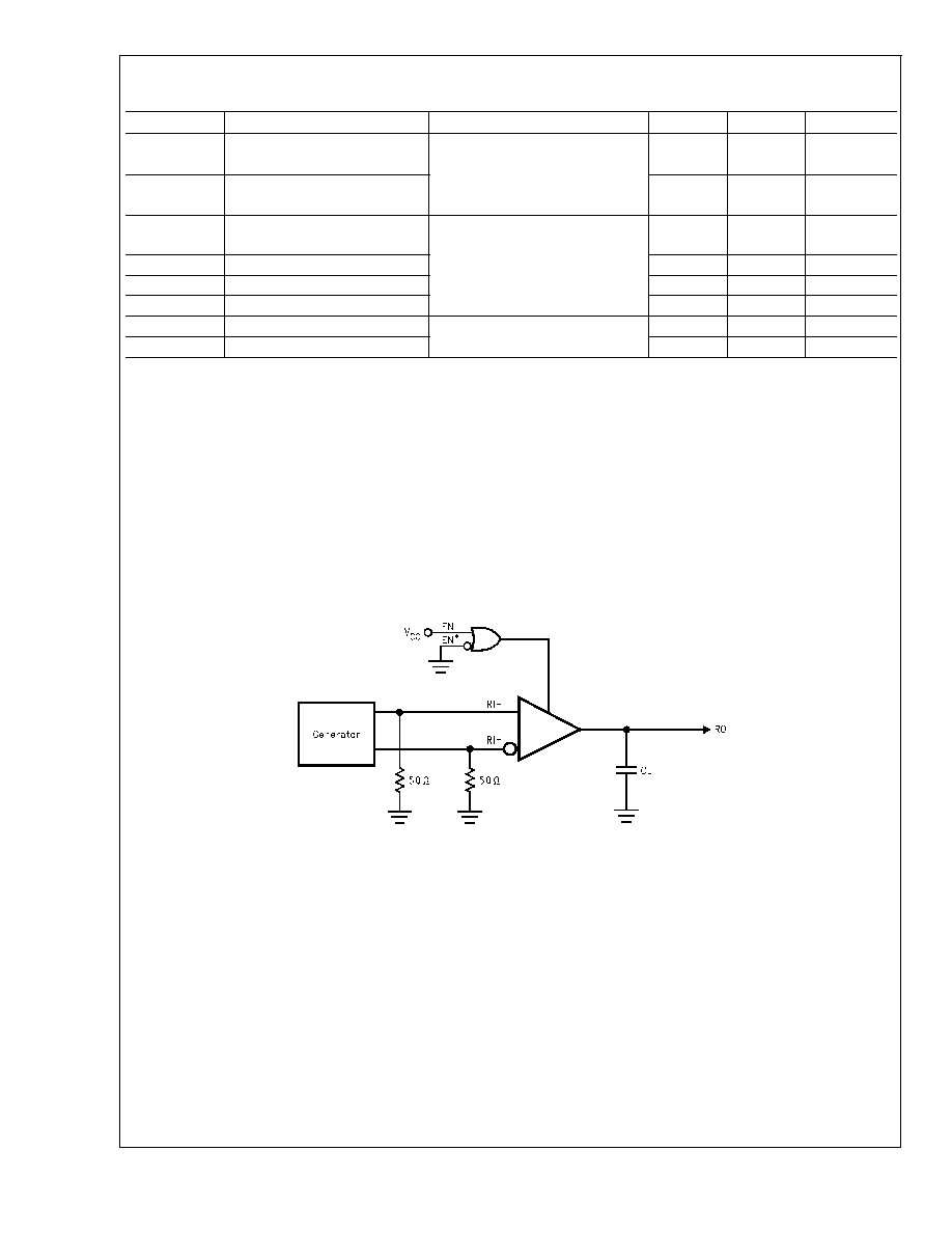
Parameter Measurement Information
01290802
FIGURE 1. Receiver Propagation Delay and Transition Time Test Circuit (Notes 10, 11)
DS26L
V32A
T
www.national.com
4
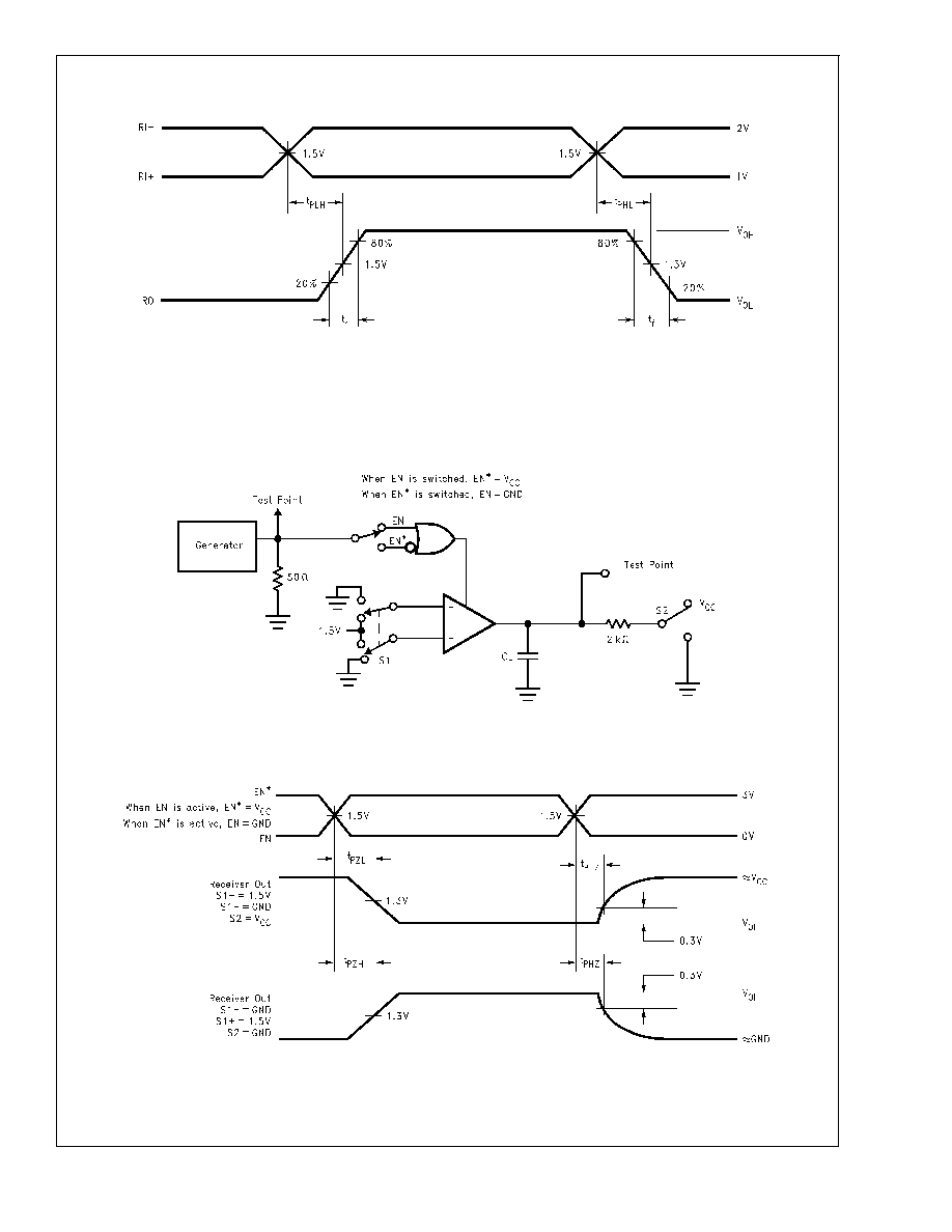
Parameter Measurement Information
(Continued)
01290803
Note 10: Generator waveform for all tests unless otherwise specified: f = 1 MHz, Duty Cycle = 50%, Z
O
= 50
, t
r
10 ns, t
f
10 ns.
Note 11: C
L
includes probe and jig capacitance.
Note 12: For military grade product, t
r
6ns and t
f
6ns.
Note 13: For military grade product the measure point is 1/2 V
CC
for t
PLH
, t
PHL
, t
PZL
, and t
PZH
FIGURE 2. Receiver Propagation Delay and Transition Time Waveform (Notes 10, 11, 12, 13)
01290804
FIGURE 3. Receiver TRI-STATE Test Circuit
01290805
FIGURE 4. Receiver TRI-STATE Output Enable and Disable Waveforms (Notes 10, 11, 12, 13)
DS26L
V32A
T
www.national.com
5