TL F 5873
DS3245
Quad
MOS
Clock
Driver
February 1986
DS3245 Quad MOS Clock Driver
General Description
The DS3245 is a quad bipolar-to-MOS clock driver with TTL
compatible inputs It is designed to provide high output cur-
rent and voltage capabilities necessary for optimum driving
of high capacitance N-channel MOS memory systems
Only 2 supplies 5 V
DC
and 12 V
DC
are required without
compromising the usual high V
OH
specification obtained by
circuits using a third supply
The device features 2 common enable inputs a refresh in-
put and a clock control input for simplified system designs
The circuit was designed for driving highly capacitive loads
at high speeds and uses Schottky-clamped transistors PNP
transistors are used on all inputs thereby minimizing input
loading
Features
Y
TTL compatible inputs
Y
Operates from 2 standard supplies 5 V
DC
12 V
DC
Y
Internal bootstrap circuit eliminates need for external
PNP's
Y
PNP inputs minimize loading
Y
High voltage current outputs
Y
Input and output clamping diodes
Y
Control logic optimized for use with MOS memory sys-
tems
Y
Pin and function equivalent to Intel 3245
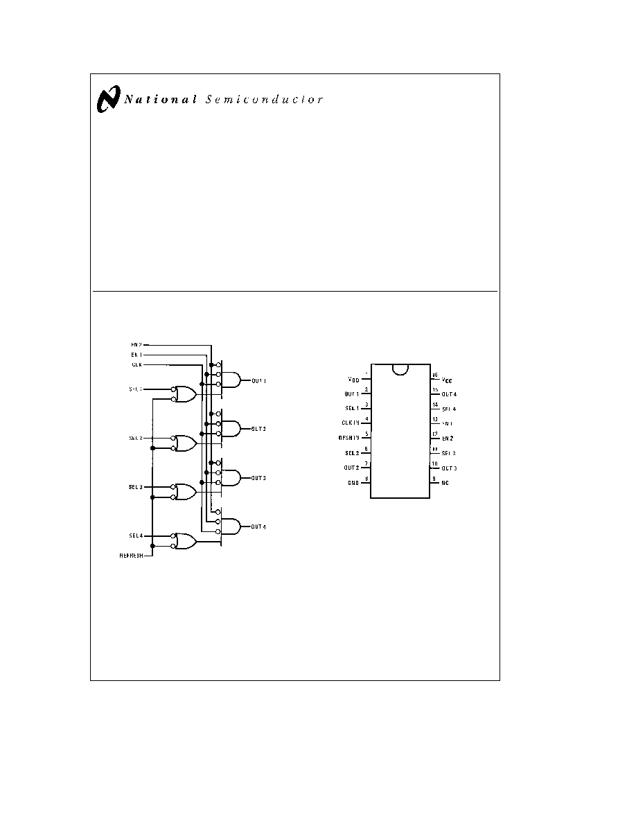
Logic and Connection Diagrams
TL F 5873 � 1
Dual-In-Line Package
TL F 5873 � 2
Top View
Order Number DS3245J or DS3245N
See NS Package Number J16A or N16A
C1995 National Semiconductor Corporation
RRD-B30M115 Printed in U S A
Absolute Maximum Ratings
If Military Aerospace specified devices are required
please contact the National Semiconductor Sales
Office Distributors for availability and specifications
Temperature Under Bias
b
10 C to
a
85 C
Storage Temperature
b
65 C to
a
150 C
Supply Voltage V
CC
b
0 5V to
a
7V
Supply Voltage V
DD
b
0 5V to
a
14V
All Input Voltages
b
1 0V to V
DD
Outputs for Clock Driver
b
1 0V to V
DD
a
1V
Maximum Power Dissipation at 25 C
Cavity Package
1509 mW
Molded Package
1476 mW
Derate cavity package 10 1 mW C above 25 C derate molded package
11 8 mW C above 25 C
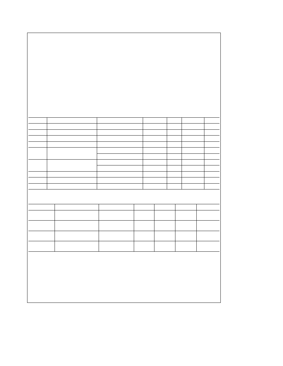
Operating Conditions
Min
Max
Units
Supply Voltage V
CC
4 75
5 25
V
Supply Voltage V
DD
11 4
12 6
V
Operating Temperature 9T
A
0
75
C
Electrical Characteristics
(Notes 2 and 3)
Symbol
Parameter
Conditions
Min
Typ
Max
Units
I
FD
Select Input Load Current
V
F
e
0 45V
b
0 25
mA
I
FE
Enable Input Load Current
V
F
e
0 45V
b
1 0
mA
I
RD
Select Input Leakage Current
V
R
e
5V
10
m
A
I
RE
Enable Input Leakage Current
V
R
e
5V
40
m
A
V
OL
Output Low Voltage
I
OL
e
5 mA V
IH
e
2V
0 45
V
I
OL
e b
5 mA
b
1 0
V
V
OH
Output High Voltage
I
OH
e b
1 mA V
IL
e
0 8V
V
DD
b
0 50
V
I
OH
e
5 mA
V
DD
a
1 0
V
V
IL
Input Low Voltage All Inputs
0 8
V
V
IH
Input High Voltage All Inputs
2
V
V
CLAMP
Input Clamp Voltage
V
CC
e
Min I
IN
e b
12 mA
b
1 0
b
1 5
V
Power Supply Current Drain
Symbol
Parameter
Conditions
Min
Typ
Max
Units
I
CC
Current from V
CC
V
CC
e
5 25V
26
34
mA
Output in High State
V
DD
e
12 6V
I
DD
Current from V
DD
V
CC
e
5 25V
23
30
mA
Output in High State
V
DD
e
12 6V
I
CC
Current from V
CC
V
CC
e
5 25V
29
39
mA
Output in Low State
V
DD
e
12 6V
I
DD
Current from V
DD
V
CC
e
5 25V
13
19
mA
Output in Low State
V
DD
e
12 6V
Note 1
``Absolute Maximum Ratings'' are those values beyond which the safety of the device cannot be guaranteed Except for ``Operating Temperature Range''
they are not meant to imply that the devices should be operated at these limits The table of ``Electrical Characteristics'' provides conditions for actual device
operation
Note 2
Unless otherwise specified min max limits apply across the 0 C to
a
C range All typical values are for T
A
e
25 C and V
CC
e
5V and V
DD
e
12V
Note 3
All currents into device pins shown as positive out of device pins as negative all voltages referenced to ground unless otherwise noted All values shown
as max or min on absolute value basis
2
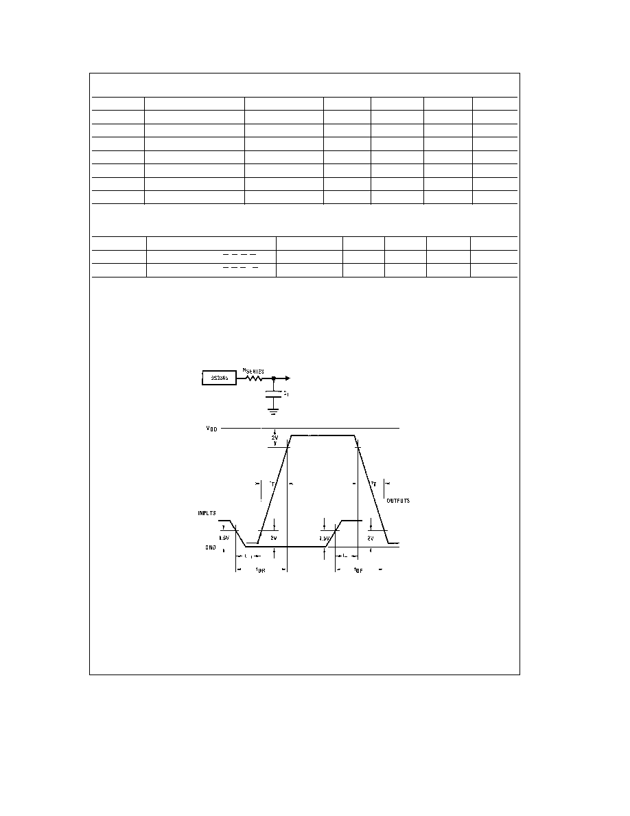
Switching Characteristics
T
A
e
0 C to
a
75 C V
CC
e
5V
g
5% V
DD
e
12V
g
5%
Symbol
Parameter
Conditions
Min
(1)
Typ
(2 4)
Max
(3)
Units
t
b a
Input to Output Delay
R
SERIES
e
0
5
11
ns
t
DR
Delay Plus Rise Time
R
SERIES
e
0
20
32
ns
t
a b
Input to Output Delay
R
SERIES
e
0
3
7
ns
t
DF
Delay Plus Fall Time
R
SERIES
e
0
18
32
ns
t
T
Output Transition Time
R
SERIES
e
20X
10
17
25
ns
t
DR
Delay Plus Rise Time
R
SERIES
e
20X
27
38
ns
t
DF
Delay Plus Fall Time
R
SERIES
e
20X
25
38
ns
Capacitance
T
A
e
25 C
(5)
Symbol
Parameter
Conditions
Min
Typ
Max
Units
C
IN
Input Capacitance I
1
I
2
I
3
I
4
5
8
pF
C
IN
Input Capacitance R C E1 E2
8
12
pF
Note 1
C
L
e
150 pF
Note 2
C
L
e
200 pF
These values represent a range of total stray plus clock capacitance for nine 4k RAMs
Note 3
C
L
e
250 pF
(
Note 4
Typical values are measured at 25 C
Note 5
This parameter is periodically sampled and is not 100% tested Condition of measurement is f
e
1 MHz V
BIAS
e
2V V
CC
e
0V and T
A
e
25 C
AC Test Circuit and Switching Time Waveforms
Input pulse amplitudes 3V
Input pulse rise and fall times
5 ns between 1V and 2V
Measurements points see waveforms
TL F 5873 � 3
TL F 5873 � 4
3
DS3245
Quad
MOS
Clock
Driver
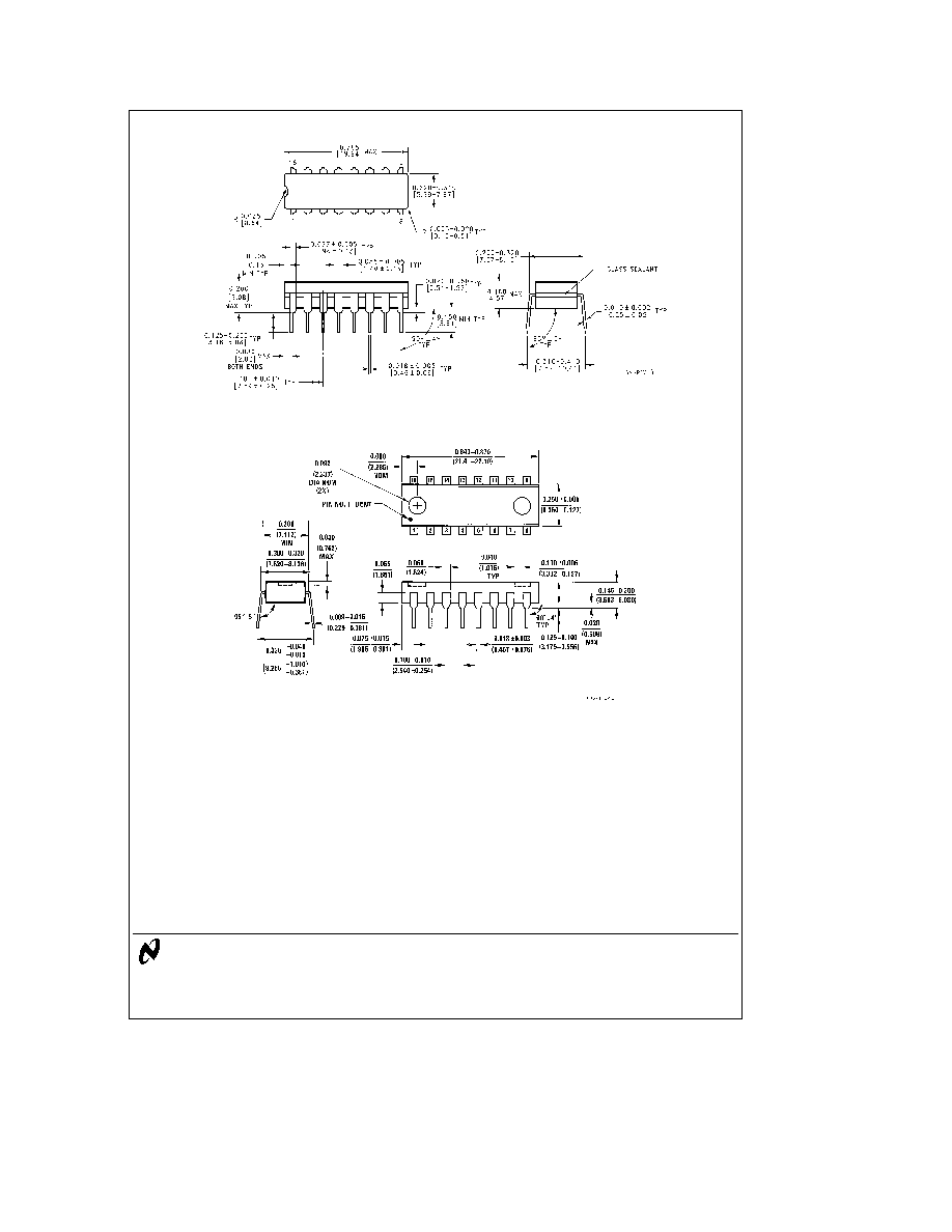
Physical Dimensions
inches (millimeters)
Ceramic Dual-in-Line Package (J)
Order Number DS3245J
NS Package Number J16A
Molded Dual-in-Line Package (N)
Order Number DS3245N
NS Package Number N16A
LIFE SUPPORT POLICY
NATIONAL'S PRODUCTS ARE NOT AUTHORIZED FOR USE AS CRITICAL COMPONENTS IN LIFE SUPPORT
DEVICES OR SYSTEMS WITHOUT THE EXPRESS WRITTEN APPROVAL OF THE PRESIDENT OF NATIONAL
SEMICONDUCTOR CORPORATION As used herein
1 Life support devices or systems are devices or
2 A critical component is any component of a life
systems which (a) are intended for surgical implant
support device or system whose failure to perform can
into the body or (b) support or sustain life and whose
be reasonably expected to cause the failure of the life
failure to perform when properly used in accordance
support device or system or to affect its safety or
with instructions for use provided in the labeling can
effectiveness
be reasonably expected to result in a significant injury
to the user
National Semiconductor
National Semiconductor
National Semiconductor
National Semiconductor
Corporation
Europe
Hong Kong Ltd
Japan Ltd
1111 West Bardin Road
Fax (a49) 0-180-530 85 86
13th Floor Straight Block
Tel 81-043-299-2309
Arlington TX 76017
Email cnjwge tevm2 nsc com
Ocean Centre 5 Canton Rd
Fax 81-043-299-2408
Tel 1(800) 272-9959
Deutsch Tel (a49) 0-180-530 85 85
Tsimshatsui Kowloon
Fax 1(800) 737-7018
English
Tel (a49) 0-180-532 78 32
Hong Kong
Fran ais Tel (a49) 0-180-532 93 58
Tel (852) 2737-1600
Italiano
Tel (a49) 0-180-534 16 80
Fax (852) 2736-9960
National does not assume any responsibility for use of any circuitry described no circuit patent licenses are implied and National reserves the right at any time without notice to change said circuitry and specifications