 | –≠–ª–µ–∫—Ç—Ä–æ–Ω–Ω—ã–π –∫–æ–º–ø–æ–Ω–µ–Ω—Ç: DS3487MX | –°–∫–∞—á–∞—Ç—å:  PDF PDF  ZIP ZIP |
DS3487
Quad TRI-STATE
Æ
Line Driver
General Description
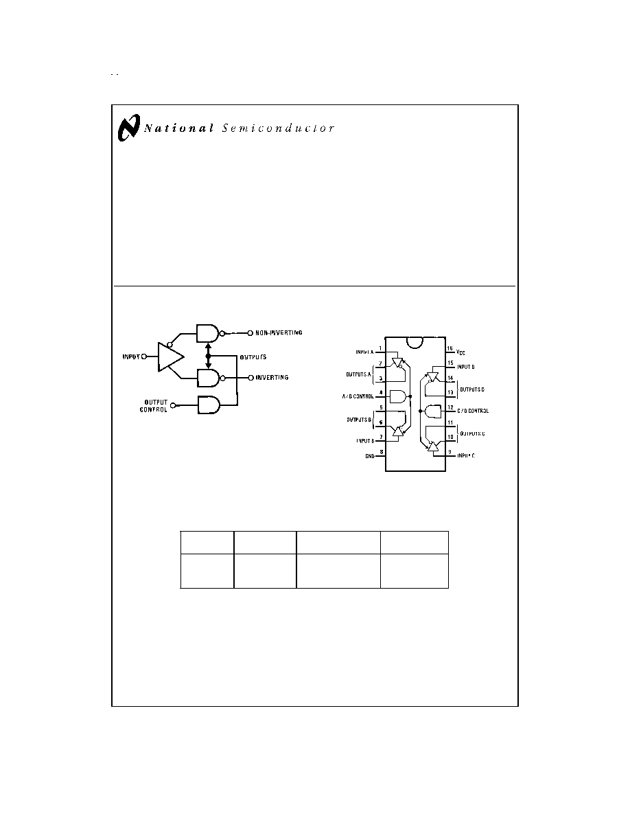
National's quad RS-422 driver features four independent
drivers which comply with EIA Standards for the electrical
characteristics of balanced voltage digital interface circuits.
The outputs are TRI-STATE structures which are forced to a
high impedance state when the appropriate output control
pin reaches a logic zero condition. All input pins are PNP
buffered to minimize input loading for either logic one or logic
zero inputs.
Features
n
Four independent drivers
n
TRI-STATE
Æ
outputs
n
Fast propagation times (typ 10 ns)
n
TTL compatible
n
5V supply
n
Output rise and fall times less than 15 ns
n
Pin compatible with DS8924 and MC3487
Block and Connection Diagrams
Truth Table
Input
Control
Non-Inverting
Inverting
Input
Output
Output
H
H
H
L
L
H
L
H
X
L
Z
Z
L = Low logic state
H = High logic state
X = Irrelevant
Z = TRI-STATE(high impedance)
TRI-STATE
Æ
is a registered trademark of National Semiconductor Corporation.
DS005780-1
Dual-In-Line Package
DS005780-2
Top View
Order Number DS3487M or DS3487N
See NS Package Number M16A or N16E
May 1998
DS3487
Quad
TRI-ST
A
T
E
Line
Driver
© 1998 National Semiconductor Corporation
DS005780
www.national.com
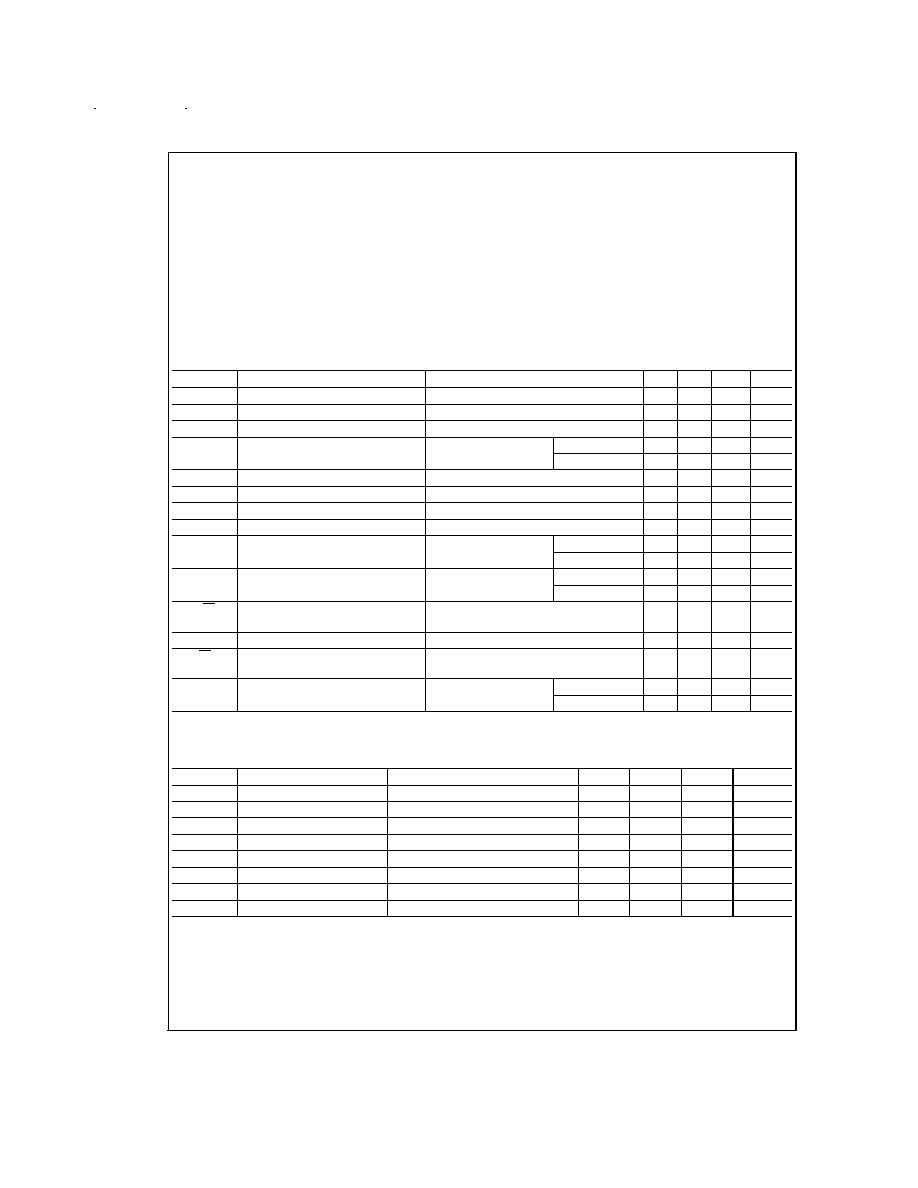
Absolute Maximum Ratings
(Note 2)
If Military/Aerospace specified devices are required,
please contact the National Semiconductor Sales Office/
Distributors for availability and specifications.
Supply Voltage
8V
Input Voltage
5.5V
Storage Temperature
-65∞C to +150∞C
Maximum Power Dissipation (Note 1) at 25∞C
Molded DIP Package
1476 mW
SO Package
1051 mW
Lead Temperature
(Soldering, 4 seconds)
260∞C
Operating Conditions
Min
Max
Units
Supply Voltage, V
CC
DS3487
4.75
5.25
V
Temperature (T
A
)
DS3487
0
+70
∞C
Note 1: Derate DIP molded package 11.9 mW/∞C above 25∞C. Derate SO
package 8.41 mW/∞C above 25∞C.
Electrical Characteristics
(Notes 3, 4, 5, 6)
Symbol
Parameter
Conditions
Min
Typ
Max
Units
V
IL
Input Low Voltage
0.8
V
V
IH
Input High Voltage
2.0
V
I
IL
Input Low Current
V
IL
= 0.5V
-200
µA
I
IH
Input High Current
V
IH
= 2.7V
50
µA
V
IH
= 5.5V
100
µA
V
CL
Input Clamp Voltage
I
CL
= -18 mA
-1.5
V
V
OL
Output Low Voltage
I
OL
= 48 mA
0.5
V
V
OH
Output High Voltage
I
OH
= -20 mA
2.5
V
I
OS
Output Short-Circuit Current
-40
-140
mA
I
OZ
Output Leakage Current
(TRI-STATE)
V
O
= 0.5V
-100
µA
V
O
= 5.5V
100
µA
I
OFF
Output Leakage Current Power OFF
V
CC
= 0V
V
O
= 6V
100
µA
V
O
= -0.25V
-100
µA
|V
OS
≠ V
OS
|
Difference in Output Offset Voltage
0.4
V
V
T
Differential Output Voltage
2.0
V
|V
T
|≠ V
T
|
Difference in Differential Output
Voltage
0.4
V
I
CC
Power Supply Current
Active
50
80
mA
TRI-STATE
Æ
35
60
mA
Switching Characteristics
V
CC
= 5V, T
A
= 25∞C
Symbol
Parameter
Conditions
Min
Typ
Max
Units
t
PHL
Input to Output
10
15
ns
t
PLH
Input to Output
10
15
ns
t
THL
Differential Fall Time
10
15
ns
t
TLH
Differential Rise Time
10
15
ns
t
PHZ
Enable to Output
R
L
= 200
, C
L
= 50 pF
17
25
ns
t
PLZ
Enable to Output
R
L
= 200
, C
L
= 50 pF
15
25
ns
t
PZH
Enable to Output
R
L
=
, C
L
= 50 pF, S1 Open
11
25
ns
t
PZL
Enable to Output
R
L
= 200
, C
L
= 50 pF, S2 Open
15
25
ns
Note 2: "Absolute Maximum Ratings" are those values beyond which the safety of the device cannot be guaranteed. They are not meant to imply that the devices
should be operated at these limits. The table of "Electrical Characteristics" provides conditions for actual device operation.
Note 3: Unless otherwise specified min/max limits apply across the 0∞C to +70∞C range for the DS3487. All typicals are given for V
CC
= 5V and T
A
= 25∞C.
Note 4: All currents into device pins are positive, all currents out of device pins as negative. All voltages are referenced to ground unless otherwise specified.
Note 5: Only one output at a time should be shorted.
Note 6: Symbols and definitions correspond to EIA RS-422, where applicable.
www.national.com
2

AC Test Circuits and Switching Time Waveforms
DS005780-3
DS005780-4
Input pulse: f = MHz, 50%; t
r
= t
f
15 ns.
FIGURE 1. Propagation Delays
DS005780-5
S1 and S2 closed except as noted.
C
L
includes probe and jig capacitance.
DS005780-6
Input pulse: f = MHz, 50%; t
r
= t
f
15 ns.
S1 = open for t
PZH
S2 = open for t
PZL
FIGURE 2. TRI-STATE Enable and Disable Delays
DS005780-7
DS005780-8
Input pulse: f = MHz, 50%; t
r
= t
f
15 ns.
FIGURE 3. Differential Rise and Fall Times
www.national.com
3

4
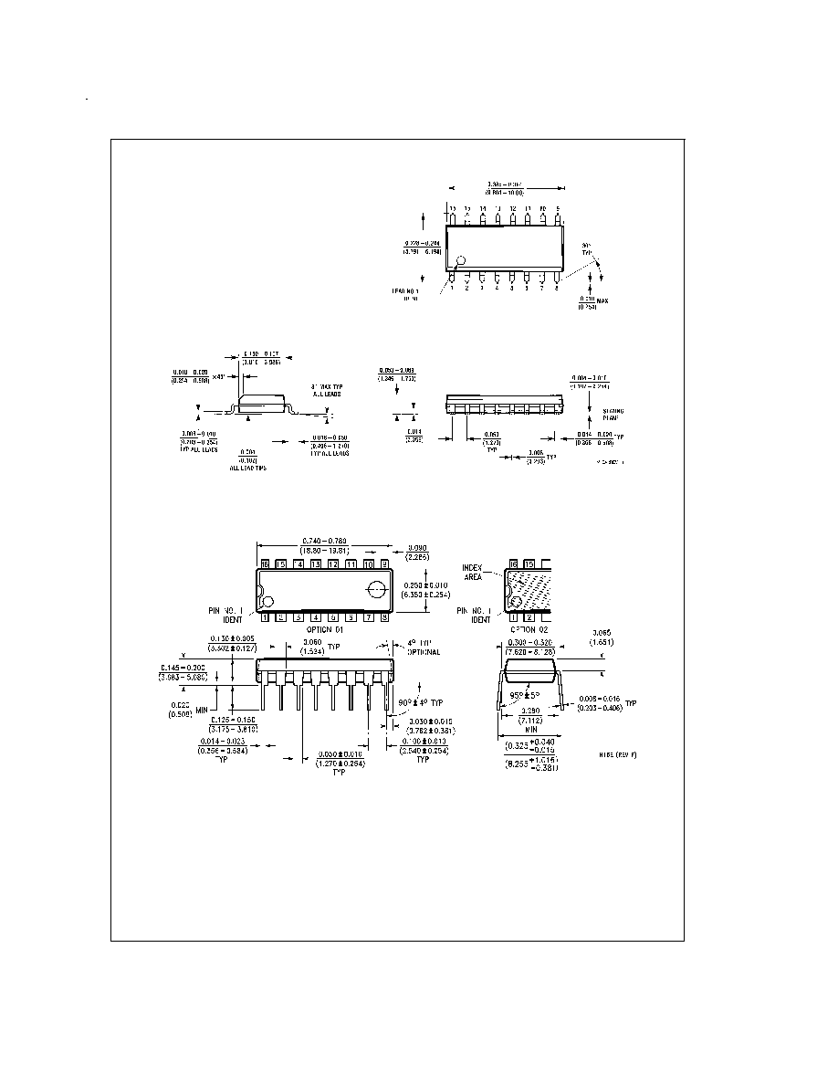
Physical Dimensions
inches (millimeters) unless otherwise noted
Small Outline Package (M)
Order Number DS3487M
NS Package Number M16A
Molded Dual-In-Line Package (N)
Order Number DS3487N
NS Package Number N16E
www.national.com
5