 | –≠–ª–µ–∫—Ç—Ä–æ–Ω–Ω—ã–π –∫–æ–º–ø–æ–Ω–µ–Ω—Ç: DS34C86TM | –°–∫–∞—á–∞—Ç—å:  PDF PDF  ZIP ZIP |

DS34C86T
Quad CMOS Differential Line Receiver
General Description
The DS34C86T is a quad differential line receiver designed
to meet the RS-422, RS-423, and Federal Standards 1020
and 1030 for balanced and unbalanced digital data transmis-
sion, while retaining the low power characteristics of CMOS.
The DS34C86T has an input sensitivity of 200 mV over the
common mode input voltage range of
±
7V. Hysteresis is pro-
vided to improve noise margin and discourage output insta-
bility for slowly changing input waveforms.
The DS34C86T features internal pull-up and pull-down resis-
tors which prevent output oscillation on unused channels.
Separate enable pins allow independent control of receiver
pairs. The TRI-STATE
Æ
outputs have 6 mA source and sink
capability. The DS34C86T is pin compatible with the
DS3486.
Features
n
CMOS design for low power
n
±
0.2V sensitivity over the input common mode voltage
range
n
Typical propagation delays: 19 ns
n
Typical input hysteresis: 60 mV
n
Inputs won't load line when V
CC
= 0V
n
Meets the requirements of EIA standard RS-422
n
TRI-STATE outputs for system bus compatibility
n
Available in surface mount
n
Open input Failsafe feature, output high for open input
Logic Diagram
Connection Diagram
Truth Table
Enable
Input
Output
L
X
Z
H
V
ID
V
TH
(Max)
H
H
V
ID
V
TH
(Min)
L
H
Open
*
H
*
Open, not terminated
Z = TRI-STATE
TRI-STATE
Æ
is a registered trademark of National Semiconductor Corporation.
DS008699-1
Dual-In-Line Package
DS008699-2
Top View
Order Number DS34C86TM, and DS34C86TN
See NS Package Number M16A and N16E
May 1998
DS34C86T
Quad
CMOS
Differential
Line
Receiver
© 1998 National Semiconductor Corporation
DS008699
www.national.com
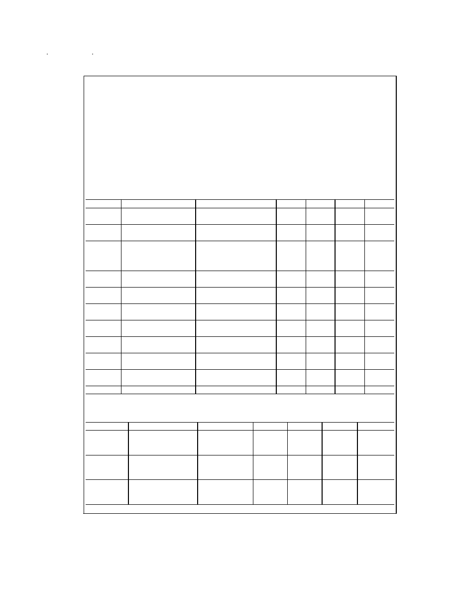
Absolute Maximum Ratings
(Notes 1, 2)
If Military/Aerospace specified devices are required,
please contact the National Semiconductor Sales Office/
Distributors for availability and specifications.
Supply Voltage (V
CC
)
7V
Input Common Mode Range (V
CM
)
±
14V
Differential Input Voltage (V
DIFF
)
±
14V
Enable Input Voltage (V
IN)
7V
Storage Temperature Range (T
STG
)
-65∞C to +150∞C
Lead Temperature (Soldering 4
sec)
260∞C
Maximum Power Dissipation at 25∞C (Note 5)
Plastic "N" Package
1645 mW
SOIC Package
1190 mW
Current Per Output
±
25 mA
This device does not meet 2000V ESD rating. (Note 4)
Operating Conditions
Min
Max
Unit
Supply Voltage (V
CC
)
4.50
5.50
V
Operating Temperature Range (T
A
)
-40
+85
∞C
Enable Input Rise or Fall Times
500
ns
DC Electrical Characteristics
(Note 3)
V
CC
= 5V
±
10% (unless otherwise specified)
Symbol
Parameter
Conditions
Min
Typ
Max
Units
V
TH
Minimum Differential
V
OUT
= V
OH
or V
OL
-200
35
+200
mV
Input Voltage
-7V
<
V
CM
<
+7V
R
IN
Input Resistance
V
IN
= -7V, +7V
5.0
6.8
10
k
(Other Input = GND)
I
IN
Input Current
V
IN
= +10V, Other Input =
GND
+1.1
+1.5
mA
(Under Test)
V
IN
= -10V, Other Input =
GND
-2.0
-2.5
mA
V
OH
Minimum High Level
V
CC
= Min., V
(DIFF)
= +1V
3.8
4.2
V
Output Voltage
I
OUT
= -6.0 mA
V
OL
Maximum Low Level
V
CC
= Max., V
(DIFF)
= -1V
0.2
0.3
V
Output Voltage
I
OUT
= 6.0 mA
V
IH
Minimum Enable High
2.0
V
Input Level Voltage
V
IL
Maximum Enable Low
0.8
V
Input Level Voltage
I
OZ
Maximum TRI-STATE
V
OUT
= V
CC
or GND,
Output Leakage Current
TRI-STATE Control = V
IL
±
0.5
±
5.0
µA
I
I
Maximum Enable Input
V
IN
= V
CC
or GND
±
1.0
µA
Current
I
CC
Quiescent Power
V
CC
= Max., V
(DIFF)
= +1V
16
23
mA
Supply Current
V
HYST
Input Hysteresis
V
CM
= 0V
60
mV
AC Electrical Characteristics
(Note 3)
V
CC
= 5V
±
10% (unless otherwise specified) (
Figures 1, 2, 3)
Symbol
Parameter
Conditions
Min
Typ
Max
Units
t
PLH
,
Propagation Delay
C
L
= 50 pF
t
PHL
Input to Output
V
DIFF
= 2.5V
19
30
ns
V
CM
= 0V
t
RISE
,
Output Rise and
C
L
= 50 pF
t
FALL
Fall Times
V
DIFF
= 2.5V
4
9
ns
V
CM
= 0V
t
PLZ
,
Propagation Delay
C
L
= 50 pF
t
PHZ
ENABLE to Output
R
L
= 1000
13
18
ns
V
DIFF
= 2.5V
www.national.com
2
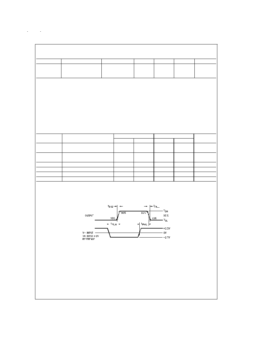
AC Electrical Characteristics
(Note 3) (Continued)
V
CC
= 5V
±
10% (unless otherwise specified) (
Figures 1, 2, 3)
Symbol
Parameter
Conditions
Min
Typ
Max
Units
t
PZL
,
Propagation Delay
C
L
= 50 pF
t
PZH
ENABLE to Output
R
L
= 1000
13
21
ns
V
DIFF
= 2.5V
Note 1: Absolute Maximum Ratings are those values beyond which the safety of the device cannot be guaranteed. They are not meant to imply that the device
should be operated at these limits. The table of "Electrical Characteristics" provides conditions for actual device operation.
Note 2: Unless otherwise specified, all voltages are referenced to ground.
Note 3: Unless otherwise specified, Min/Max limits apply across the operating temperature range.
All typicals are given for V
CC
= 5V and T
A
= 25∞C.
Note 4: ESD Rating; HBM (1.5k
, 100 pF)
Inputs
2000V
All other pins
1000V
EIAJ (0
, 200 pF)
350V
Note 5: Ratings apply to ambient temperature at 25∞C. Above this temperature derate N Package 13.16 mW/∞C, and M Package 9.52 mW/∞C.
Comparison Table of Switching Characteristics into "LS-Type" Load
(Note 6)
V
CC
= 5V, T
A
= 25∞C (Figures 4, 5)
Symbol
Parameter
DS34C86
DS3486
Units
Typ
Max
Typ
Max
t
PHL(D)
Propagation Delay Time
17
19
ns
Output High to Low
t
PLH(D)
Propagation Delay Time
19
19
ns
Output Low to High
t
PLZ
Output Low to TRI-STATE
13
23
ns
t
PHZ
Output High to TRI-STATE
12
25
ns
t
PZH
Output TRI-STATE to High
13
18
ns
t
PZL
Output TRI-STATE to Low
13
20
ns
Note 6: This Table is provided for comparison purposes only. The values in this table for the DS34C86 reflect the performance of the device but are not tested or
guaranteed.
Test and Switching Waveforms
DS008699-3
FIGURE 1. Propagation Delays
www.national.com
3
Test and Switching Waveforms
(Continued)
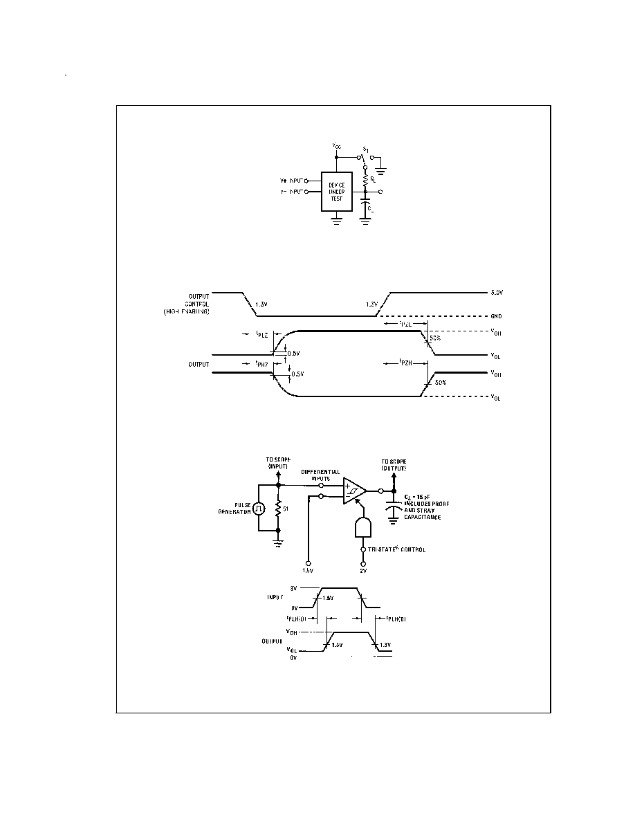
AC Test Circuits and Switching Time Waveforms
DS008699-4
C
L
Includes load and test jig capacitance.
S1 = V
CC
for t
PZL
, and t
PLZ
measurements.
S1 = GND for t
PZH
, and t
PHZ
measurements.
FIGURE 2. Test Circuit for TRI-STATE Output Tests
DS008699-5
FIGURE 3. TRI-STATE Output Enable and Disable Waveforms
DS008699-6
DS008699-7
Input Pulse Characteristics:
t
TLH
= t
THL
= 6 ns (10% to 90%)
PRR = 1 MHz, 50% duty cycle
FIGURE 4. Propagation Delay Differential Input to Output for "LS-Type" Load
www.national.com
4
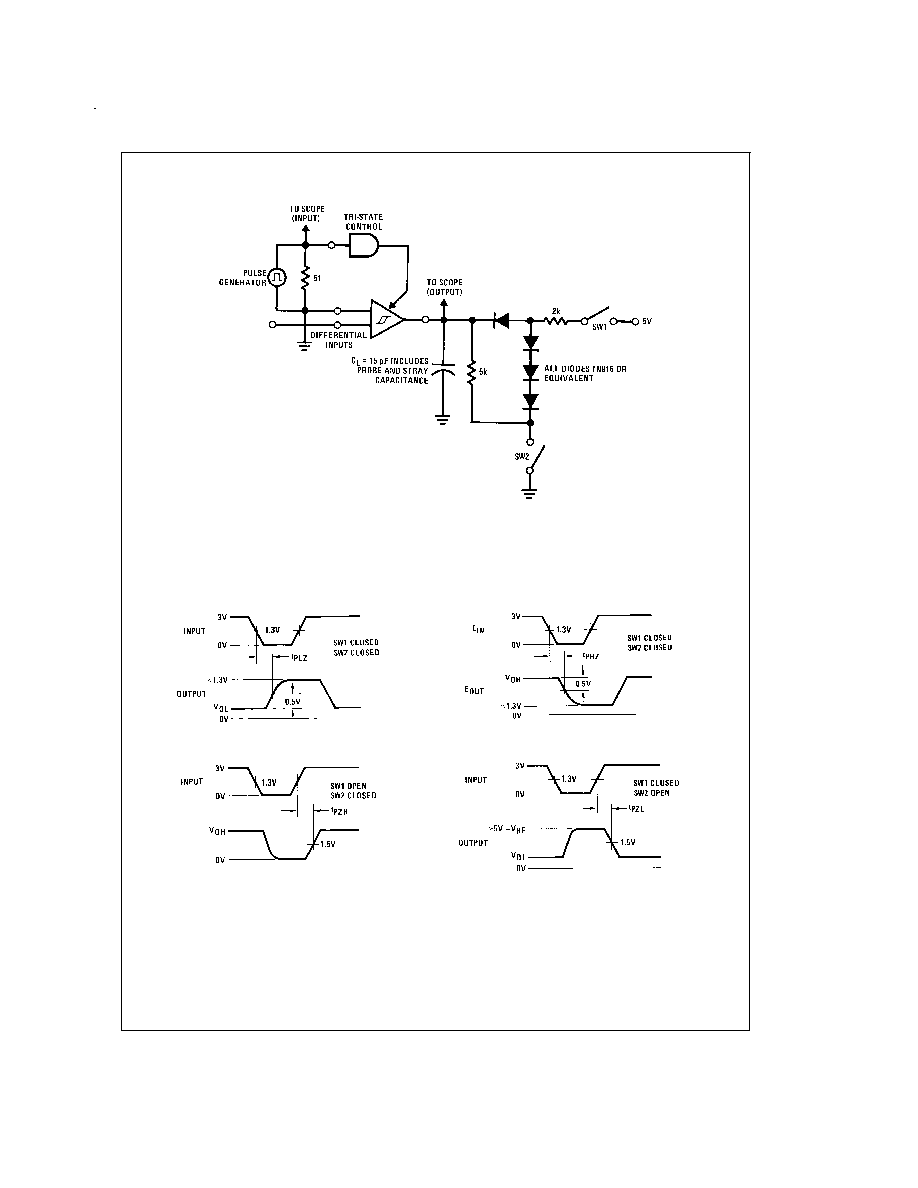
AC Test Circuits and Switching Time Waveforms
(Continued)
DS008699-8
1.5V for t
PHZ
and t
PLZ
-1.5V for t
PLZ
and t
PZL
Input Pulse Characteristics:
t
TLH
= t
THL
= 6 ns (10% to 90%)
PRR = 1 MHz, 50% duty cycle
t
PLZ
DS008699-9
t
PHZ
DS008699-10
t
PZH
DS008699-11
t
PZL
DS008699-12
FIGURE 5. Propagation Delay TRI-STATE Control Unit to Output for "LS-Type" Load
www.national.com
5