DS34C87T CMOS Quad TRI-STATE Differential Line Driver
DS34C87T
CMOS Quad TRI-STATE Differential Line Driver
General Description
The DS34C87T is a quad differential line driver designed for
digital
data
transmission
over
balanced
lines.
The
DS34C87T meets all the requirements of EIA standard
RS-422 while retaining the low power characteristics of
CMOS. This enables the construction of serial and terminal
interfaces while maintaining minimal power consumption.
The DS34C87T accepts TTL or CMOS input levels and
translates these to RS-422 output levels. This part uses
special output circuitry that enables the individual drivers to
power down without loading down the bus. This device has
separate enable circuitry for each pair of the four drivers.
The DS34C87T is pin compatible to the DS3487T.
All inputs are protected against damage due to electrostatic
discharge by diodes to V
CC
and ground.
Features
n
TTL input compatible
n
Typical propagation delays: 6 ns
n
Typical output skew: 0.5 ns
n
Outputs won't load line when V
CC
= 0V
n
Meets the requirements of EIA standard RS-422
n
Operation from single 5V supply
n
TRI-STATE outputs for connection to system buses
n
Low quiescent current
n
Available in surface mount
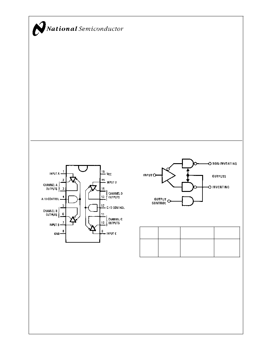
Connection and Logic Diagrams
Dual-In-Line Package
00857601
See Pin Description Table for details
Top View
Order Number DS34C87TM or DS34C87TN
See NS Package Number M16A or N16E
00857602
Truth Table
Input
Control
Non-Inverting
Inverting
Input
Output
Output
H
H
H
L
L
H
L
H
X
L
Z
Z
L = Low logic state
H = High logic state
X = Irrelevant
Z = TRI-STATE (high performance)
April 2002
DS34C87T
CMOS
Quad
TRI-ST
A
T
E
Differential
Line
Driver
� 2002 National Semiconductor Corporation
DS008576
www.national.com
Absolute Maximum Ratings
(Notes 1,
2)
If Military/Aerospace specified devices are required,
please contact the National Semiconductor Sales Office/
Distributors for availability and specifications.
Supply Voltage (V
CC
)
-0.5 to 7.0V
DC Voltage (V
IN
)
-1.5 to V
CC
+1.5V
DC Output Voltage (V
OUT
)
-0.5 to 7V
Clamp Diode Current (I
IK
, I
OK
)
�
20 mA
DC Output Current, per pin (I
OUT
)
�
150 mA
DC V
CC
or GND Current (I
CC
)
�
150 mA
Storage Temperature Range (T
STG
)
-65�C to
+150�C
Maximum Power Dissipation (P
D
)
@
25�C (Note
3)
Plastic "N" Package
1736 mW
SOIC Package
1226 mW
Lead Temperature (T
L
)
(Soldering 4 sec)
260�C
This device does not meet 2000V ESD rating. (Note 12)
Operating Conditions
Min Max Units
Supply Voltage (V
CC
)
4.50 5.50
V
DC Input or Output Voltage (V
IN
, V
OUT
)
0
V
CC
V
Operating Temperature Range (T
A
)
DS34C87T
-40 +85
�C
Input Rise or Fall Times (t
r
, t
f
)
500
ns
DC Electrical Characteristics
(Note 4)
V
CC
= 5V
�
10% (unless otherwise specified)
Symbol
Parameter
Conditions
Min
Typ
Max
Units
V
IH
High Level Input
2.0
V
Voltage
V
IL
Low Level Input
0.8
V
Voltage
V
OH
High Level Output
V
IN
= V
IH
or V
IL
,
2.5
3.4
V
Voltage
I
OUT
= -20 mA
V
OL
Low Level Output
V
IN
= V
IH
or V
IL
,
0.3
0.5
V
Voltage
I
OUT
= 48 mA
V
T
Differential Output
R
L
= 100
2.0
3.1
V
Voltage
(Note 5)
|V
T
|�| V
T
|
Difference In
R
L
= 100
0.4
V
Differential Output
(Note 5)
V
OS
Common Mode
R
L
= 100
2.0
3.0
V
Output Voltage
(Note 5)
|V
OS
� V
OS
|
Difference In
R
L
= 100
0.4
V
Common Mode Output
(Note 5)
I
IN
Input Current
V
IN
= V
CC
, GND, V
IH
, or V
IL
�
1.0
�A
I
CC
Quiescent Supply
I
OUT
= 0 �A,
Current
V
IN
= V
CC
or GND
200
500
�A
V
IN
= 2.4V or 0.5V (Note 6)
0.8
2.0
mA
I
OZ
TRI-STATE
TM
Output
V
OUT
= V
CC
or GND
�
0.5
�
5.0
�A
Leakage Current
Control = V
IL
I
SC
Output Short
V
IN
= V
CC
or GND
-30
-150
mA
Circuit Current
(Notes 5, 7)
I
OFF
Power Off Output
V
CC
= 0V
V
OUT
= 6V
100
�A
Leakage Current
(Note 5)
V
OUT
= -0.25V
-100
�A
Note 1: Absolute Maximum Ratings are those values beyond which the safety of the device cannot be guaranteed. They are not meant to imply that the device
should be operated at these limits. The table of "Electrical Characteristics" provide conditions for actual device operation.
Note 2: Unless otherwise specified, all voltages are referenced to ground. All currents into device pins are positive; all currents out of device pins are negative.
Note 3: Ratings apply to ambient temperature at 25�C. Above this temperature derate N Package 13.89 mW/�C, and M Package 9.80 mW/�C.
Note 4: Unless otherwise specified, min/max limits apply across the -40�C to 85�C temperature range. All typicals are given for V
CC
= 5V and T
A
= 25�C.
Note 5: See EIA Specification RS-422 for exact test conditions.
DS34C87T
www.national.com
2
DC Electrical Characteristics
(Note 4) (Continued)
Note 6: Measured per input. All other inputs at V
CC
or GND.
Note 7: This is the current sourced when a high output is shorted to ground. Only one output at a time should be shorted.
Switching Characteristics
(Note 4)
V
CC
= 5V
�
10%, t
r
, t
f
6 ns (
Figures 1, 2, 3, 4)
Symbol
Parameter
Conditions
Min
Typ
Max
Units
t
PLH
, t
PHL
Propagation Delay
S1 Open
6
11
ns
Input to Output
Skew
(Note 8)
S1 Open
0.5
3
ns
t
TLH
, t
THL
Differential Output Rise
S1 Open
6
10
ns
And Fall Times
t
PZH
Output Enable Time
S1 Closed
12
25
ns
t
PZL
Output Enable Time
S1 Closed
13
26
ns
t
PHZ
Output Disable Time (Note 9)
S1 Closed
4
8
ns
t
PLZ
Output Disable Time (Note 9)
S1 Closed
6
12
ns
C
PD
Power Dissipation
100
pF
Capacitance (Note 10)
C
IN
Input Capacitance
6
pF
Note 8: Skew is defined as the difference in propagation delays between complementary outputs at the 50% point.
Note 9: Output disable time is the delay from the control input being switched to the output transistors turning off. The actual disable times are less than indicated
due to the delay added by the RC time constant of the load.
Note 10: C
PD
determines the no load dynamic power consumption, P
D
= C
PD
V
2
CC f + I
CC
V
CC
, and the no load dynamic current consumption, I
S
= C
PD
V
CC
f
+ I
CC
.
Comparison Table of Switching Characteristics into "LS-Type" Load
(Note 11)
V
CC
= 5V, T
A
= +25�C, t
r
6 ns, t
f
6 ns (
Figures 4, 5, 6, 7, 8, 9)
Symbol
Parameter
Conditions
DS34C87
DS3487
Units
Typ
Max
Typ
Max
t
PLH
, t
PHL
Propagation Delay
6
10
10
15
ns
Input to Output
Skew
(Note 8)
1.5
2.0
ns
t
THL
, t
TLH
Differential Output Rise
4
7
10
15
ns
and Fall Times
t
PHZ
Output Disable Time
C
L
= 50 pF, R
L
= 200
,
8
11
17
25
ns
(Note 9)
S1 Closed, S2 Closed
t
PLZ
Output Disable Time
C
L
= 50 pF, R
L
= 200
,
7
10
15
25
ns
(Note 9)
S1 Closed, S2 Closed
t
PZH
Output Enable Time
C
L
= 50 pF, R
L
=
,
11
19
11
25
ns
S1 Open, S2 Closed
t
PZL
Output Enable Time
C
L
= 50 pF, R
L
= 200
,
14
21
15
25
ns
S1 Closed, S2 Open
Note 11: This table is provided for comparison purposes only. The values in this table for the DS34C87 reflect the performance of the device but are not tested or
guaranteed.
Note 12: ESD Rating: HBM (1.5 k
, 100 pF)
Inputs
1500V
Outputs
1000V
EIAJ (0
, 200 pF)
All Pins
350V
DS34C87T
www.national.com
3
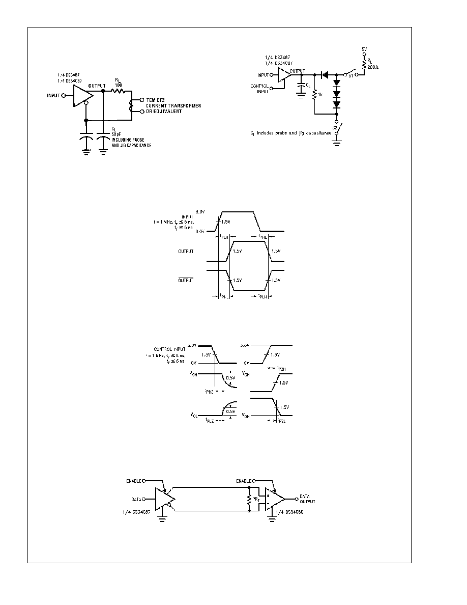
AC Test Circuit and Switching Time Waveforms
00857603
Note: C1 = C2 = C3 = 40 pF (including Probe and Jig Capacitance), R1 = R2 = 50
, R3 = 500
FIGURE 1. AC Test Circuit
00857604
FIGURE 2. Propagation Delays
00857605
FIGURE 3. Enable and Disable Times
00857607
Input pulse; f = 1 MHz, 50%, t
r
6 ns, t
f
6 ns
FIGURE 4. Differential Rise and Fall Times
00857608
FIGURE 5. Propagation Delays Test Circuit
for "LS-Type" Load
DS34C87T
www.national.com
4
AC Test Circuit and Switching
Time Waveforms
(Continued)
Typical Applications
00857612
*R
T
is optional although highly recommended to reduce reflection.
00857606
FIGURE 6. Differential Rise and Fall Times
Test Circuit for "LS-Type" Load
00857609
FIGURE 7. Load Enable and Disable Times
Test Circuit for "LS-Type" Load
00857610
FIGURE 8. Load Propagation Delays for "LS-Type" Load
00857611
FIGURE 9. Load Enable and Disable Times for "LS-Type" Load
DS34C87T
www.national.com
5
Document Outline