DS36277
Dominant Mode Multipoint Transceiver
General Description
The DS36277 Dominant Mode Multipoint Transceiver is de-
signed for use on bi-directional differential busses. It is opti-
mal for use on Interfaces that utilize Society of Automotive
Engineers (SAE) J1708 Electrical Standard.
The device is similar to standard TIA/EIA-485 transceivers,
but differs in enabling scheme. The Driver's Input is normally
externally tied LOW, thus providing only two states: Active
(LOW), or Disabled (OFF). When the driver is active, the
dominant mode is LOW, conversely, when the driver is dis-
abled, the bus is pulled HIGH by external bias resistors.
The receiver provides a FAILSAFE feature that guarantees a
known output state when the Interface is in the following con-
ditions: Floating Line, Idle Line (no active drivers), and Line
Fault Conditions (open or short). The receiver output is
HIGH for the following conditions: Open Inputs, Terminated
Inputs (50
), or Shorted Inputs. FAILSAFE is a highly desir-
able feature when the transceivers are used with Asynchro-
nous Controllers such as UARTs.
Features
n
FAILSAFE receiver, RO = HIGH for:
-- OPEN inputs
-- Terminated inputs
-- SHORTED inputs
n
Optimal for use in SAE J1708 Interfaces
n
Compatible with popular interface standards:
-- TIA/EIA-485 and TIA/EIA-422-A
-- CCITT recommendation V.11
n
Bi-directional transceiver
-- Designed for multipoint transmission
n
Wide bus common mode range
-- (-7V to +12V)
n
Available in plastic DIP and SOIC packages
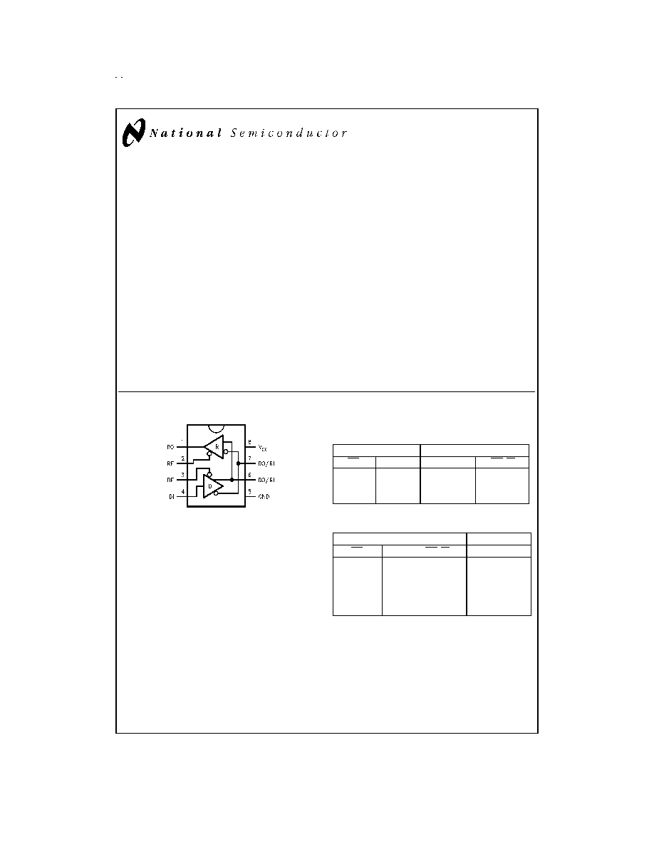
Connection and Logic Diagram
Truth Tables
Driver
Inputs
Outputs
DE
DI
DO/RI
DO /RI
L
L
L
H
L
H
H
L
H
X
Z
Z
Receiver
Inputs
Output
RE
DO/RI�DO /RI
RO
L
0 mV
H
L
-500 mV
L
L
SHORTED
H
L
OPEN
H
H
X
Z
TRI-STATE
�
is a registered trademark of National Semiconductor Corporation.
DS011384-1
Order Number DS36277TM or DS36277TN
See NS Package Number M08A or N08E
July 1998
DS36277
Dominant
Mode
Multipoint
T
ransceiver
� 1999 National Semiconductor Corporation
DS011384
www.national.com
Absolute Maximum Ratings
(Note 1)
If Military/Aerospace specified devices are required,
please contact the National Semiconductor Sales Office/
Distributors for availability and specifications.
Supply Voltage (V
CC
)
7V
Input Voltage (DE , RE , and DI)
5.5V
Driver Output Voltage/
Receiver Input Voltage
-10V to +15V
Receiver Output Voltage (RO)
5.5V
Maximum Package Power Dissipation
@
+25�C
N Package
(derate 9.3 mW/�C above +25�C)
1168 mW
M Package
(derate 5.8 mW/�C above +25�C)
726 mW
Storage Temperature Range
-65�C to +150�C
Lead Temperature (Soldering 4 sec.)
260�C
ESD Rating (HBM, 1.5 k
, 100 pF)
6.0 kV
Recommended Operating
Conditions
Min
Max
Units
Supply Voltage, V
CC
4.75
5.25
V
Bus Voltage
-7
+12
V
Operating Temperature (T
A
)
DS36277T
-40
+85
�C
Electrical Characteristics
(Notes 2, 4)
Over recommended Supply Voltage and Operating Temperature ranges, unless otherwise specified.
Symbol
Parameter
Conditions
Min
Typ
Max
Units
DRIVER CHARACTERISTICS
V
OD
Differential Output Voltage
I
O
= 0 mA (No Load)
1.5
3.6
6
V
V
oDO
Output Voltage
I
O
= 0 mA (Output to GND)
0
6
V
V
oDO
Output Voltage
0
6
V
V
T1
Differential Output Voltage
(Termination Load)
R
L
= 54
(485)
(
Figure 1 )
1.3
2.2
5.0
V
R
L
= 100
(422)
1.7
2.6
5.0
V
V
T1
Balance of V
T1
R
L
= 54
(Note 3)
-0.2
0.2
V
|V
T1
- V
T1
|
R
L
= 100
-0.2
0.2
V
V
OS
Driver Common Mode
Output Voltage
R
L
= 54
(
Figure 1 )
0
2.5
3.0
V
R
L
= 100
0
2.5
3.0
V
V
OS
Balance of V
OS
R
L
= 54
(Note 3)
-0.2
0.2
V
|V
OS
- V
OS
|
R
L
= 100
-0.2
0.2
V
V
OH
Output Voltage High
I
OH
= -22 mA
(
Figure 2 )
2.7
3.7
V
V
OL
Output Voltage Low
I
OL
= +22 mA
1.3
2
V
I
OSD
Driver Short-Circuit
Output Current
V
O
= +12V
(
Figure 3 )
92
290
mA
V
O
= -7V
-187
-290
mA
RECEIVER CHARACTERISTICS
V
TH
Differential Input High
Threshold Voltage (Note 5)
V
O
= V
OH
, I
O
= -0.4 mA
-0.150
0
V
-7V
V
CM
+12V
V
TL
Differential Input Low
Threshold Voltage (Note 5)
V
O
= V
OL
, I
O
= 8.0 mA
-0.5
-0.230
V
-7V
V
CM
+12V
V
HST
Hysteresis (Note 6)
V
CM
= 0V
80
mV
I
IN
Line Input Current
(V
CC
= 4.75V, 5.25V, 0V)
Other Input = 0V
V
I
= +12V
0.5
1.5
mA
DE = V
IH
(Note 7)
V
I
= -7V
-0.5
-1.5
mA
I
OSR
Short Circuit Current
V
O
= 0V
RO
-15
-32
-85
mA
I
OZ
TRI-STATE
�
Leakage Current
V
O
= 0.4 to 2.4V
-20
1.4
+20
�A
V
OH
Output High Voltage
(
Figure 12 )
V
ID
= 0V, I
OH
= -0.4 mA
2.3
3.7
V
V
ID
= OPEN, I
OH
= -0.4 mA
2.3
3.7
V
V
OL
Output Low Voltage
(
Figure 12 )
V
ID
= -0.5V, I
OL
= +8 mA
0.3
0.7
V
V
ID
= -0.5V, I
OL
= +16 mA
0.3
0.8
V
R
IN
Input Resistance
10
20
k
www.national.com
2
Electrical Characteristics
(Notes 2, 4) (Continued)
Over recommended Supply Voltage and Operating Temperature ranges, unless otherwise specified.
Symbol
Parameter
Conditions
Min
Typ
Max
Units
DEVICE CHARACTERISTICS
V
IH
High Level Input Voltage
DE ,
RE ,
or
DI
2.0
V
CC
V
V
IL
Low Level Input Voltage
GND
0.8
V
I
IH
High Level Input Current
V
IH
= 2.4V
20
�A
I
IL
Low Level Input Current
V
IL
= 0.4V
-100
�A
V
CL
Input Clamp Voltage
I
CL
= -18 mA
-0.7
-1.5
V
I
CC
Output Low Voltage
DE = 0V, RE = 0V, DI = 0V
39
60
mA
I
CCR
Supply Current
DE = 3V, RE = 0V, DI = 0V
24
50
mA
I
CCD
(No Load)
DE = 0V, RE = 3V, DI = 0V
40
75
mA
I
CCX
DE = 3V, RE = 3V, DI = 0V
27
45
mA
Switching Characteristics
(Note 4)
Over recommended Supply Voltage and Operating Temperature ranges, unless otherwise specified.
Symbol
Parameter
Conditions
Min
Typ
Max
Units
DRIVER CHARACTERISTICS
t
PLHD
Diff. Prop. Delay Low to High
R
L
= 54
8
17
60
ns
t
PHLD
Diff. Prop. Delay High to Low
C
L
= 50 pF
8
19
60
ns
t
SKD
Diff. Skew (|t
PLHD
�t
PHLD
|)
C
D
= 50 pF
2
10
ns
t
r
Diff. Rise Time
(
Figures 4, 5 )
11
60
ns
t
f
Diff. Fall Time
11
60
ns
t
PLH
Prop. Delay Low to High
R
L
= 27
, C
L
= 15 pF
22
85
ns
t
PHL
Prop. Delay High to Low
(
Figures 6, 7 )
25
85
ns
t
PZH
Enable Time Z to High
R
L
= 110
25
60
ns
t
PZL
Enable Time Z to Low
C
L
= 50 pF
30
60
ns
t
PHZ
Disable Time High to Z
(
Figure 8 � Figure 11 )
16
60
ns
t
PLZ
Disable Time Low to Z
11
60
ns
RECEIVER CHARACTERISTICS
t
PLH
Prop. Delay Low to High
V
ID
= -1.5V to +1.5V
15
37
90
ns
t
PHL
Prop. Delay High to Low
C
L
= 15 pF
15
43
90
ns
t
SK
Skew (|t
PLH
�t
PHL
|)
(
Figures 13, 14 )
6
15
ns
t
PZH
Enable Time Z to High
C
L
= 15 pF
12
60
ns
t
PZL
Enable Time Z to Low
(
Figures 15, 16 )
28
60
ns
t
PHZ
Disable Time High to Z
20
60
ns
t
PLZ
Disable Time Low to Z
10
60
ns
Note 1: "Absolute Maximum Ratings" are those values beyond which the safety of the device cannot be guaranteed. They are not meant to imply that the devices
should be operated at these limits. The tables of "Electrical Characteristics" specify conditions for device operation.
Note 2: Current into device pins is defined as positive. Current out of device pins is defined as negative. All voltages are referenced to ground unless otherwise speci-
fied.
Note 3:
|V
T1
| and
|V
OS
| are changes in magnitude of V
T1
and V
OS
, respectively, that occur when the input changes state.
Note 4: All typicals are given for V
CC
= 5.0V and T
A
= +25�C.
Note 5: Threshold parameter limits specified as an algebraic value rather than by magnitude.
Note 6: Hysteresis defined as V
HST
= V
TH
- V
TL
.
Note 7: I
IN
includes the receiver input current and driver TRI-STATE leakage current.
www.national.com
3
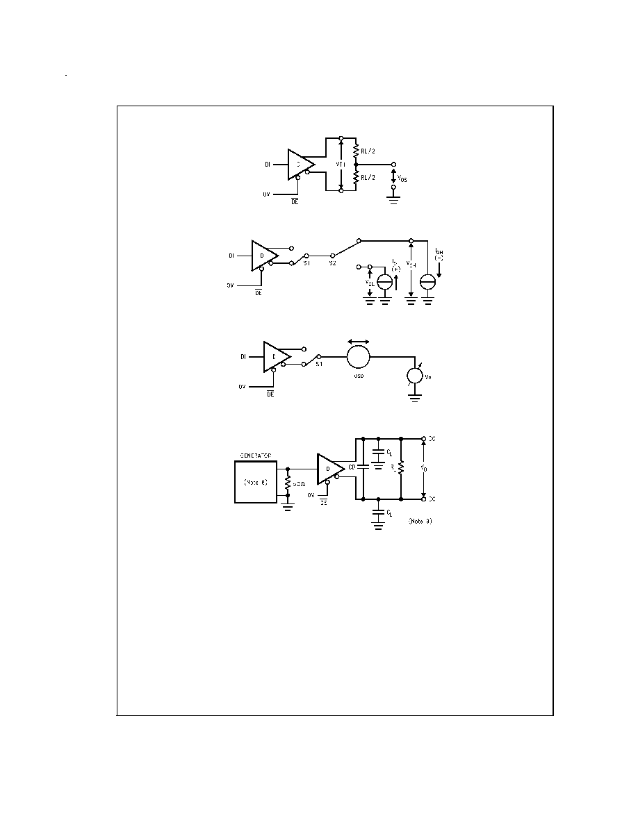
Parameter Measurement Information
DS011384-2
FIGURE 1. Driver V
T1
and V
OS
Test Circuit
DS011384-3
FIGURE 2. Driver V
OH
and V
OL
Test Circuit
DS011384-4
FIGURE 3. Driver Short Circuit Test Circuit
DS011384-5
FIGURE 4. Driver Differential Propagation Delay and Transition Time Test Circuit
www.national.com
4
Parameter Measurement Information
(Continued)
DS011384-6
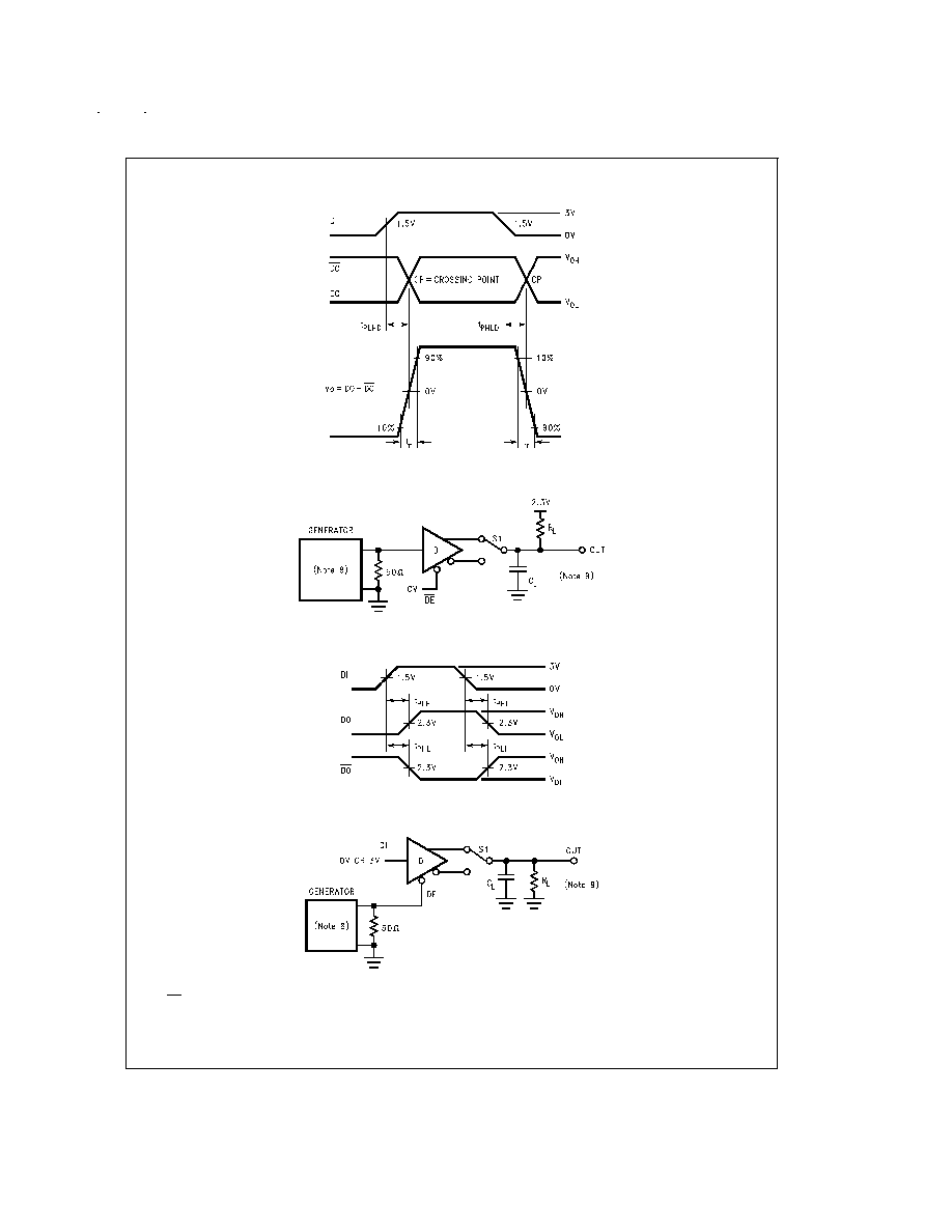
FIGURE 5. Driver Differential Propagation Delays and Transition Times
DS011384-7
FIGURE 6. Driver Propagation Delay Test Circuit
DS011384-8
FIGURE 7. Driver Propagation Delays
DS011384-9
S1 to DO for DI = 3V
S1 to DO for DI = 0V
FIGURE 8. Driver TRl-STATE Test Circuit (t
PZH
, t
PHZ
)
www.national.com
5