TL F 5816
DS1631DS3631DS1632DS3632DS1633DS3633DS1634DS3634
CMOS
Dual
Peripheral
Drivers
July 1992
DS1631 DS3631 DS1632 DS3632 DS1633 DS3633
DS1634 DS3634 CMOS Dual Peripheral Drivers
General Description
The DS1631 series of dual peripheral drivers was designed
to be a universal set of interface components for CMOS
circuits
Each circuit has CMOS compatible inputs with thresholds
that track as a function of V
CC
(approximately
V
CC
) The
inputs are PNPs providing the high impedance necessary
for interfacing with CMOS
Outputs have high voltage capability minimum breakdown
voltage is 56V at 250 mA
The outputs are Darlington connected transistors This al-
lows high current operation (300 mA max) at low internal
V
CC
current levels since base drive for the output transistor
is obtained from the load in proportion to the required load-
ing conditions This is essential in order to minimize loading
on the CMOS logic supply
Typical V
CC
e
5V power is 28 mW with both outputs ON
V
CC
operating range is 4 5V to 15V
The circuit also features output transistor protection if the
V
CC
supply is lost by forcing the output into the high impe-
dance OFF state with the same breakdown levels as when
V
CC
was applied
Pin-outs are the same as the respective logic functions
found in the following popular series of circuits DS75451
DS75461 This feature allows direct conversion of present
systems to the MM74C CMOS family and DS1631 series
circuits with great power savings
The DS1631 series is also TTL compatible at V
CC
e
5V
Features
Y
CMOS compatible inputs
Y
High impedance inputs
PNP's
Y
High output voltage breakdown
56V min
Y
High output current capability
300 mA max
Y
Same pin-outs and logic functions as DS75451 and
DS75461 series circuits
Y
Low V
CC
power dissipation (28 mW both outputs ``ON''
at 5V)
Connection Diagrams
(Dual-In-Line and Metal Can Packages)
TL F 5816 ≠ 1
Top View
Order Number DS1631J-8
or DS3631N
TL F 5816 ≠ 2
Top View
Order Number DS1632J-8
or DS3632N
TL F 5816 ≠ 3
Top View
Order Number DS1633J-8
or DS3633N
TL F 5816 ≠ 4
Top View
Order Number DS1634J-8
or DS3634N
See NS Package Number J08A or N08E
TL F 5816 ≠ 5
Top View
(Pin 4 is electrically connected to the
case )
Order Number DS1631H
TL F 5816 ≠ 6
Top View
(Pin 4 is electrically connected to the
case )
Order Number DS1632H
TL F 5816 ≠ 7
Top View
(Pin 4 is electrically connected to the
case )
Order Number DS1633H
TL F 5816 ≠ 8
Top View
(Pin 4 is electrically connected to the
case )
Order Number DS1634H
See NS Package Number H08C
C1995 National Semiconductor Corporation
RRD-B30M105 Printed in U S A
Absolute Maximum Ratings
(Note 1)
If Military Aerospace specified devices are required
please contact the National Semiconductor Sales
Office Distributors for availability and specifications
Supply Voltage
16V
Voltage at Inputs
b
0 3V to V
CC
a
0 3V
Output Voltage
56V
Storage Temperature Range
b
65 C to
a
150 C
Maximum Power Dissipation at 25 C
Cavity Package
1133 mW
Molded Package
1022 mW
TO-5 Package
787 mW
Lead Temperature (Soldering 4 sec
260 C
Derate cavity package 7 6 mW C above 25 C derate molded package
8 2 mW C above 25 C derate TO-5 package 5 2 mW C above 25 C
Operating Conditions
Min
Max
Units
Supply Voltage V
CC
DS1631 DS1632
4 5
15
V
DS1633 DS1634
DS3631 DS3632
4 75
15
V
DS3633 DS3634
Temperature T
A
DS1631 DS1632
b
55
a
125
C
DS1633 DS1634
DS3631 DS3632
0
a
70
C
DS3633 DS3634
Electrical Characteristics
(Notes 2 and 3)
Symbol
Parameter
Conditions
Min
Typ
Max
Units
ALL CIRCUITS
V
IH
Logical ``1'' Input Voltage
(
Figure 1 )
V
CC
e
5V
3 5
2 5
V
V
CC
e
10V
8 0
5
V
V
CC
e
15V
12 5
7 5
V
V
IL
Logical ``0'' Input Voltage
(
Figure 1 )
V
CC
e
5V
2 5
1 5
V
V
CC
e
10V
5 5
2 0
V
V
CC
e
15V
7 5
2 5
V
I
IH
Logical ``1'' Input Current
V
CC
e
15V V
IN
e
15V (
Figure 2 )
0 1
10
m
A
I
IL
Logical ``0'' Input Current
V
IN
e
0 4V (
Figure 3 )
V
CC
e
5V
b
50
b
120
m
A
V
CC
e
15V
b
200
b
360
m
A
V
OH
Output Breakdown Voltage V
CC
e
15V I
OH
e
250 mA (
Figure 1 )
56
65
V
V
OL
Output Low Voltage
V
CC
e
Min (
Figure 1 )
DS1631 DS1632
I
OL
e
100 mA
0 85
1 1
V
DS1633 DS1634
I
OL
e
300 mA
1 1
1 4
V
V
CC
e
Min (
Figure 1 )
DS3631 DS3632
I
OL
e
100 mA
0 85
1 0
V
DS3633 DS3634
I
OL
e
300 mA
1 1
1 3
V
DS1631 DS3631
I
CC(0)
Supply Currents
V
IN
e
0V (
Figure 4)
V
CC
e
5V
Output Low
7
11
mA
V
CC
e
15V
Both Drivers
14
20
mA
I
CC(1)
(
Figure 4 )
V
CC
e
5V V
IN
e
5V
Output High
2
3
mA
V
CC
e
15V V
IN
e
15V Both Drivers
7 5
10
mA
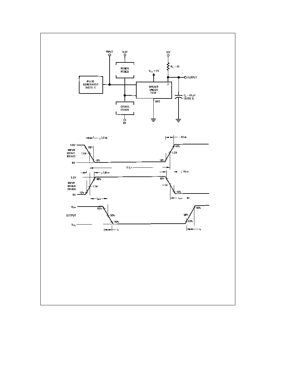
t
PD1
Propagation to ``1''
V
CC
e
5V T
A
e
25 C C
L
e
15 pF R
L
e
50X V
L
e
10V
500
ns
(
Figure 5 )
t
PD0
Propagation to ``0''
V
CC
e
5V T
A
e
25 C C
L
e
15 pF R
L
e
50X V
L
e
10V
750
ns
(
Figure 5 )
DS1632 DS3632
I
CC(0)
Supply Currents
(
Figure 4 )
V
CC
e
5V V
IN
e
5V
Output Low
8
12
mA
V
CC
e
15V V
IN
e
15V
18
23
mA
I
CC(1)
V
IN
e
0V (
Figure 4 )
V
CC
e
5V
Output High
2 5
3 5
mA
V
CC
e
15V
9
14
mA
t
PD1
Propagation to ``1''
V
CC
e
5V T
A
e
25 C C
L
e
15 pF R
L
e
50X V
L
e
10V
500
ns
(
Figure 5 )
t
PD0
Propagation to ``0''
V
CC
e
5V T
A
e
25 C C
L
e
15 pF R
L
e
50X V
L
e
10V
750
ns
(
Figure 5 )
2
Electrical Characteristics
(Notes 2 and 3) (Continued)
Symbol
Parameter
Conditions
Min
Typ
Max
Units
DS1633 DS3633
I
CC(0)
Supply Currents
V
IN
e
0V (
Figure 4 )
V
CC
e
5V
Output Low
7 5
12
mA
V
CC
e
15V
16
23
mA
I
CC(1)
(
Figure 4 )
V
CC
e
5V V
IN
e
5V
Output High
2
4
mA
V
CC
e
15V V
IN
e
15V
7 2
15
mA
t
PD1
Propagation to ``1''
V
CC
e
5V T
A
e
25 C C
L
e
15 pF R
L
e
50X V
L
e
10V
500
ns
(
Figure 5 )
t
PD0
Propagation to ``0''
V
CC
e
5V T
A
e
25 C C
L
e
15 pF R
L
e
50X V
L
e
10V
750
ns
(
Figure 5 )
DS1634 DS3634
I
CC(0)
Supply Currents
(
Figure 4 )
V
CC
e
5V V
IN
e
5V
Output Low
7 5
12
mA
V
CC
e
15V V
IN
e
15V
18
23
mA
I
CC(1)
V
IN
e
0V (
Figure 4 )
V
CC
e
5V
Output High
3
5
mA
V
CC
e
15V
11
18
mA
t
PD1
Propagation to ``1''
V
CC
e
5V T
A
e
25 C C
L
e
15 pF R
L
e
50X V
L
e
10V
500
ns
(
Figure 5 )
t
PD0
Propagation to ``0''
V
CC
e
5V T
A
e
25 C C
L
e
15 pF R
L
e
50X V
L
e
10V
750
ns
(
Figure 5 )
Note 1
``Absolute Maximum Ratings'' are those values beyond which the safety of the device cannot be guaranteed Except for ``Operating Temperature Range''
they are not meant to imply that the devices should be operated at these limits The table of ``Electrical Characteristics'' provides conditions for actual device
operation
Note 2
Unless otherwise specified min max limits apply across the
b
55 C to
a
125 C temperature range for the DS1631 DS1632 DS1633 and DS1634 and
across the 0 C to
a
70 C range for the DS3631 DS3632 DS3633 and DS3634 All typical values are for T
A
e
25 C
Note 3
All currents into device pins shown as positive out of device pins as negative all voltages referenced to ground unless otherwise noted All values shown
as max or min on absolute value basis
Test Circuits
TL F 5816 ≠ 9
Input
Other
Output
Circuit
Under
Input
Apply
Measure
Test
DS3631
V
IH
V
IH
I
OH
V
OH
V
IL
V
CC
I
OL
V
OL
DS3632
V
IH
V
IH
I
OL
V
OL
V
IL
V
CC
I
OH
V
OH
DS3633
V
IH
GND
I
OH
V
OH
V
IL
V
IL
I
OL
V
OL
DS3634
V
IH
GND
I
OL
V
OL
V
IL
V
IL
I
OH
V
OH
Note
Each input is tested separately
FIGURE 1 V
IH
V
IL
V
OH
V
OL
3

Test Circuits
(Continued)
TL F 5816 ≠ 10
Each input is tested separately
FIGURE 2 I
IH
TL F 5816 ≠ 11
Note A
Each input is tested separately
Note B
When testing DS1633 and DS1634 input not under test is grounded
For all other circuits it is at V
CC
FIGURE 3 I
IL
TL F 5816 ≠ 12
Both gates are tested simultaneously
FIGURE 4 I
CC
for AND and NAND Circuits
Schematic Diagram
(Equivalent Circuit)
TL F 5816 ≠ 15
4