 | –≠–ª–µ–∫—Ç—Ä–æ–Ω–Ω—ã–π –∫–æ–º–ø–æ–Ω–µ–Ω—Ç: DS3647A | –°–∫–∞—á–∞—Ç—å:  PDF PDF  ZIP ZIP |
TL F 8354
DS3647A
Quad
TRI-STATE
MOS
Memory
IO
Register
February 1986
DS3647A Quad TRI-STATE
MOS Memory I O Register
General Description
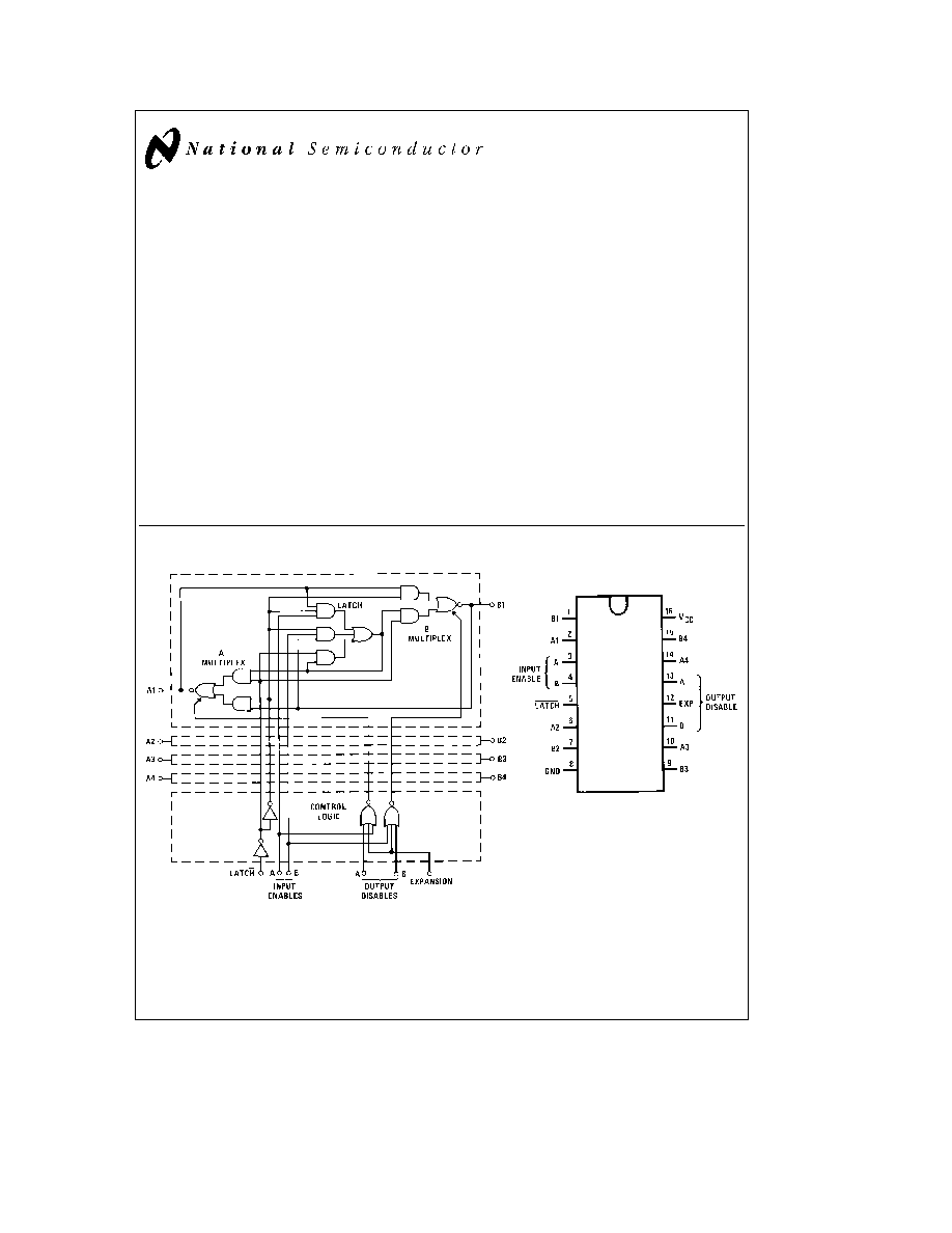
The DS3647A is a 4-bit I O buffer register intended for use
in MOS memory systems This circuit employs a fall-through
latch for data storage This method of latching captures the
data in parallel with the output thus eliminating the delays
encountered in other designs This circuit uses Schottky-
clamped transistor logic for minimum propagation delay and
employs PNP input transistors so that input currents are
low allowing a large fan-out for this circuit which is needed
in a memory system
Two pins per bit are provided and data transfer is bi-direc-
tional so that the register can handle both input and output
data The direction of data flow is controlled through the
input enables The latch control when taken low will cause
the register to hold the data present at that time and display
it at the outputs Data can be latched into the register inde-
pendent of the output disables or EXPANSION input Either
or both of the outputs may be taken to the high-impedance
state with the output disables The EXPANSION pin dis-
ables both outputs to facilitate multiplexing with other I O
registers on the same data lines
The DS3647A features TRI-STATE outputs The ``B'' port
outputs are designed for use in bus organized data trans-
mission systems and can sink 80 mA and source
b
5 2 mA
Data going from port ``A'' to port ``B'' and from ``B'' to port
``A'' is inverted in the DS3647A
Features
Y
PNP inputs minimize loading
Y
Fall-through latch design
Y
Propagation delay of only 15 ns
Y
TRI-STATE outputs
Y
EXPANSION control
Y
Bi-directional data flow
Y
TTL compatible
Y
Transmission line driver output
Logic and Connection Diagrams
TL F 8354 ≠ 1
Dual-In-Line Package
TL F 8354 ≠ 2
Top View
Order Number DS3647AD or DS3647AN
See NS Package Number D16C or N16A
TRI-STATE
is a registered trademark of National Semiconductor Corp
C1995 National Semiconductor Corporation
RRD-B30M105 Printed in U S A
Absolute Maximum Ratings
(Note 1)
If Military Aerospace specified devices are required
please contact the National Semiconductor Sales
Office Distributors for availability and specifications
Supply Voltage
7V
Input Voltage
b
1 5V to
a
7V
Storage Temperature Range
b
65 to
a
150 C
Maximum Power Dissipation at 25 C
Molded Package
1476 mW
Lead Temperature (Soldering 10 seconds)
300 C
Derate molded package 10 0 mW
C above 25 C
Operating Conditions
Min
Max
Units
Supply Voltage (V
CC
)
4 5
5 5
V
Temperature (T
A
)
DS3647A
0
a
70
C
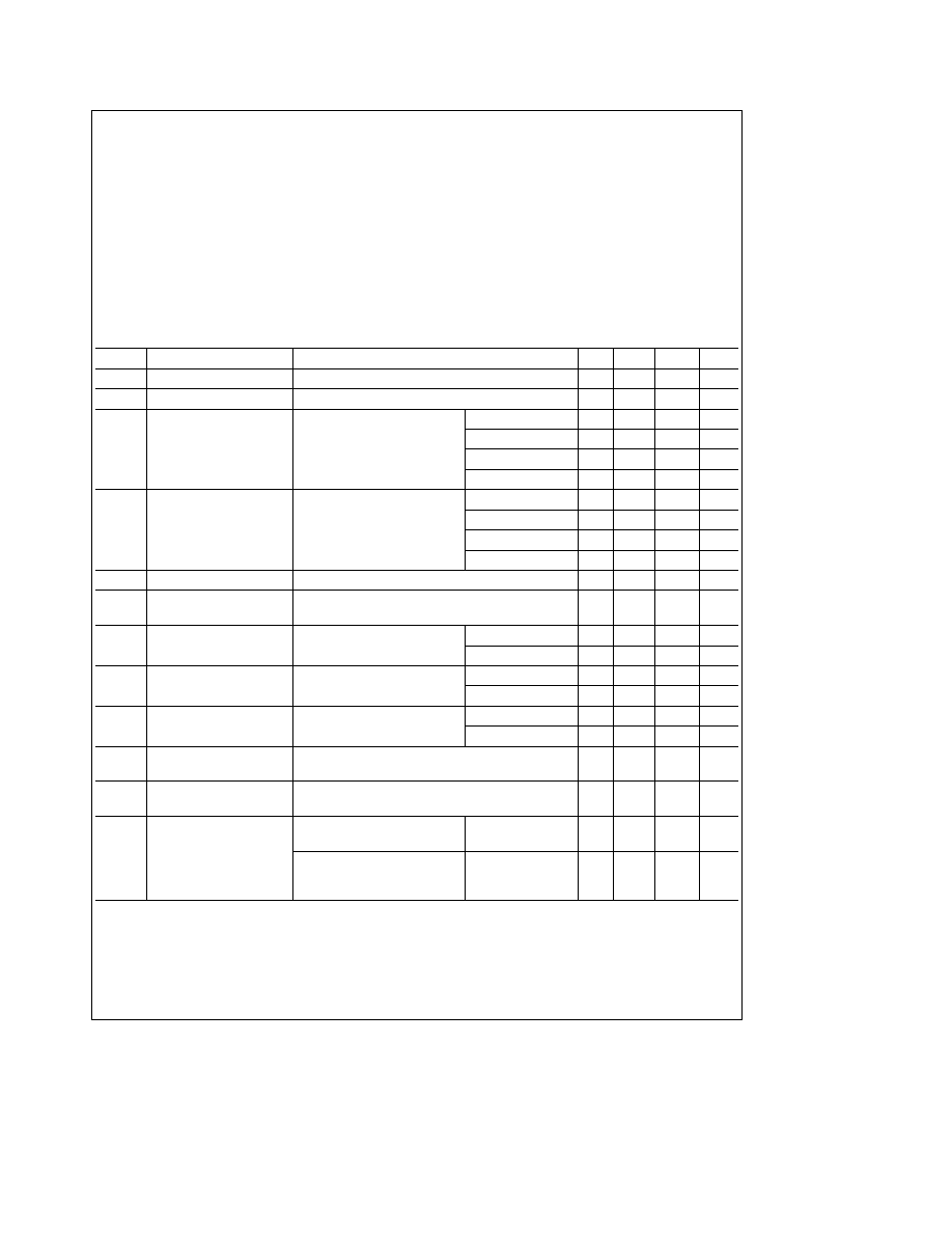
Electrical Characteristics
(Notes 2 and 3)
Symbol
Parameter
Conditions
Min
Typ
Max
Units
V
IN(1)
Logic ``1'' Input Voltage
2 0
V
V
IN(0)
Logic ``0'' Input Voltage
0 8
V
I
IN(1)
Logic ``1'' Input Current
Latch Disable Inputs
0 1
40
m
A
V
CC
e
5 5V V
IN
e
5 5V
Expansion
0 2
80
m
A
A Ports B Ports
0 2
100
m
A
Enable Inputs
0 4
200
m
A
I
IN(0)
Logic ``0'' Input Current
Latch Disable Inputs
b
25
b
250
m
A
V
CC
e
5 5V V
IN
e
0 5V
Expansion
b
50
b
500
m
A
A Ports B Ports
b
50
b
500
m
A
Enable Inputs
b
0 1
b
1 25
mA
V
CLAMP
Input Clamp Voltage
V
CC
e
4 5V I
IN
e b
18 mA
b
0 6
b
1 2
V
V
OL(A)
Logic ``0'' Output Voltage
V
CC
e
4 5V I
OL
e
20 mA
0 4
0 5
V
A Ports
V
OL(B)
Logic ``0'' Output Voltage
V
CC
e
4 5V
I
OL
e
30 mA
0 3
0 4
V
B Ports
I
OL
e
50 mA
0 4
0 5
V
V
OH(A)
Logic ``1'' Output Voltage
I
OH
e b
1 mA
V
CC
e
5V
3 0
3 4
V
A Ports
V
CC
e
4 5V
2 5
3 4
V
V
OH(B)
Logic ``1'' Output Voltage
I
OH
e b
5 2 mA (Note 4)
V
CC
e
5V
2 9
3 3
V
B Ports
V
CC
e
4 5V
2 4
3 3
V
I
OS(A)
Output Short-Circuit Current
V
CC
e
4 5V to 5 5V V
OUT
e
0V (Note 4)
b
50
b
80
b
120
mA
A Port
I
OS(B)
Output Short-Circuit Current
V
CC
e
4 5V to 5 5V V
OUT
e
0V (Note 4)
b
70
b
120
b
180
mA
B Port
I
CC
Power Supply Current
Exp
e
3V A Ports
e
0V
B Ports Open All Other Pins
e
0V
DS3647A
100
140
mA
Enable A Latch
e
3V A Ports
e
0V B Ports Open All Other
DS3647A
70
105
mA
Pins
e
0V
Note 1
``Absolute Maximum Ratings'' are those values beyond which the safety of the device cannot be guaranteed Except for ``Operating Temperature Range''
they are not meant to imply that the devices should be operated at these limits The table of ``Electrical Characteristics'' provides conditions for actual device
operation
Note 2
Unless otherwise specified min max limits apply across the 0 C to
a
70 C range All typicals are given for V
CC
e
5V and T
A
e
25 C
Note 3
All currents into device pins shown as positive out of device pins as negative all voltages referenced to ground unless otherwise noted
Note 4
Only one output at a time should be shorted
2

Switching Characteristics
(V
CC
e
5V T
A
e
25 C)
Symbol
Parameter
Conditions
Min
Typ
Max
Units
DATA TRANSFER B PORT TO A PORT
t
pd0
Propagation Delay to a Logic ``0''
CL
e
50 pF R
L
e
280X
7 5
15
ns
(Figures 1 and 4)
t
pd1
Propagation Delay to a Logic ``1''
C
L
e
50 pF R
L
e
280X
6 0
12
ns
(Figures 1 and 4)
A PORT CONTROL FROM OUTPUT DISABLE A INPUT
t
LZ
Delay to High Impedance from
(Figures 1 and 5)
13
20
ns
Logic ``0''
t
HZ
Delay to High Impedance from
(Figures 1 and 6)
14
20
ns
Logic ``1''
t
ZL
Delay to Logic ``0'' from High
(Figures 1 and 7)
10
15
ns
Impedance
t
ZH
Delay to Logic ``1'' from High
(Figures 1 and 8)
25
35
ns
Impedance
DATA TRANSFER A PORT TO B PORT DS3647A
t
pd0
Propagation Delay to a Logic ``0''
C
L
e
50 pF R
L
e
100 X
6 5
12
ns
(Figures 2 and 4)
t
pd1
Propagation Delay to a Logic ``1''
C
L
e
50 pF R
L
e
100 X
8 0
15
ns
(Figures 2 and 4)
B PORT CONTROL FROM OUTPUT DISABLE B INPUT DS3647A
t
LZ
Delay to High Impedance from
(Figures 2 and 5)
15
25
ns
Logic ``0''
t
HZ
Delay to High Impedance from
(Figures 2 and 6)
14
20
ns
Logic ``1''
t
ZL
Delay to Logic ``0'' from High
(Figures 2 and 7)
10
16
ns
Impedance
t
ZH
Delay to Logic ``1'' from High
(Figures 2 and 8)
25
35
ns
Impedance
LATCH SET-UP AND HOLD TIMES ALL DEVICES
t
SET-UP
Set-Up Time of Data Input Before
5
0
ns
Latch Goes Low
t
HOLD
Hold Time of Data Input After
10
5
ns
Latch Goes Low
Product Description
Device Number
B Port To A Port
A Port To B Port
A Port Outputs
B Port Outputs
Function
Function
DS3647A
Inverting
Inverting
TRI-STATE
TRI-STATE
3

Truth Table
Input
Output
A Ports
B Ports
Enables
Latch
Disables
Expansion
A1-A4
B1-B4
Comments
A
B
A
B
1
0
1
0
0
0
Hi-Z
A
Data in on A output to B
0
1
1
0
0
0
B
Hi-Z
Data in on B output to A
1
0
0
0
0
0
Hi-Z
A
Data stored which is present
when latch goes low
0
1
0
0
0
0
B
Hi-Z
Data stored which is present
when latch goes low
1
0
x
0
1
0
Hi-Z
Hi-Z
Both A and B in Hi-Z state
Data in on A may be latched
0
1
x
1
0
0
Hi-Z
Hi-Z
Both A and B in Hi-Z state
Data in on B may be latched
x
x
x
x
x
1
Hi-Z
Hi-Z
Both A and B in Hi-Z state
AC Test Circuits
TL F 8354 ≠ 3
FIGURE 1 A Port Load
TL F 8354 ≠ 4
FIGURE 2 B Port Load
Note 1
C
L
includes probe and jig capacitance
Operating Waveforms
Using TRI-STATE
TL F 8354 ≠ 5
TRI-STATE Disabled
TL F 8354 ≠ 6
When the Input Enable makes a negative transition the output will be indeterminate for a short duration The negative transition of the Input Enable normally
occurs during a don't-care timing state at the output
4
Switching Time Waveforms
t
pd0
and t
pd1
TL F 8354 ≠ 7
Input Characteristics f
e
1 MHz t
R
e
t
F
s
5 ns (10% to 90% points) duty cycle
e
50% Z
OUT
e
50 X
FIGURE 4
t
LZ
TL F 8354 ≠ 8
FIGURE 5
t
ZL
TL F 8354 ≠ 9
FIGURE 7
t
HZ
TL F 8354 ≠ 10
FIGURE 6
t
ZH
TL F 8354 ≠ 11
FIGURE 8
Schematic Diagram
TL F 8354 ≠ 12
Note
Data pins A1≠A4 and B1≠B4 consist of
an input and an output tied together
5