 | –≠–ª–µ–∫—Ç—Ä–æ–Ω–Ω—ã–π –∫–æ–º–ø–æ–Ω–µ–Ω—Ç: DS3651N | –°–∫–∞—á–∞—Ç—å:  PDF PDF  ZIP ZIP |
DS1651/DS3651
Quad High Speed MOS Sense Amplifiers
General Description
The DS1651/DS3651 is TTL compatible high speed circuits
intended for sensing in a broad range of MOS memory sys-
tem applications. Switching speeds have been enhanced
over conventional sense amplifiers by application of Schot-
tky technology, and TRI-STATE
Æ
strobing is incorporated, of-
fering a high impedance output state for bused organization.
The DS1651/DS3651 has active pull-up outputs and offers
open collector outputs providing implied "AND" operations.
Features
n
High speed
n
TTL compatible
n
Input sensitivity --
±
7 mV
n
TRI-STATE outputs for high speed buses
n
Standard supply voltages --
±
5V
n
Pin and function compatible with MC3430
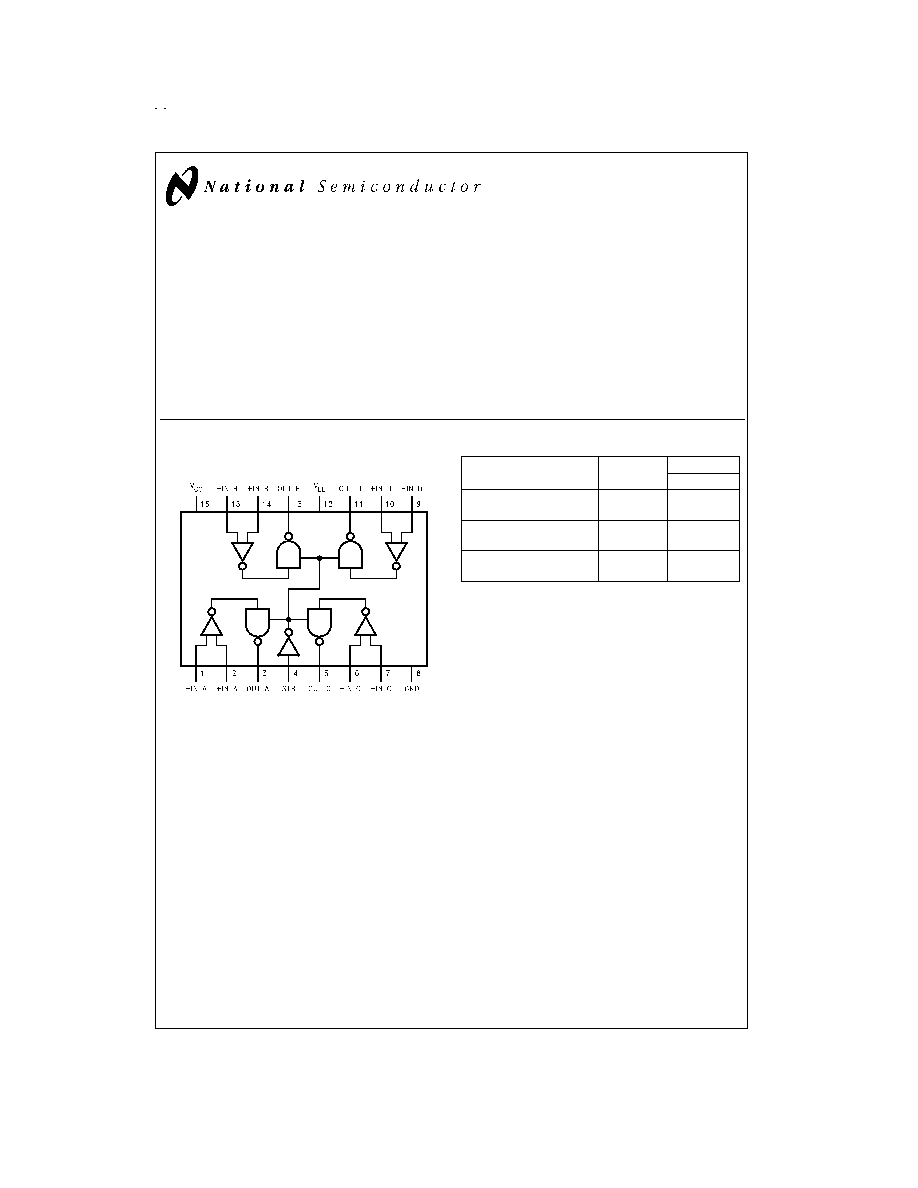
Connection Diagram
Truth Table
Input
Strobe
Output
DS3651
V
ID
7 mW
T
A
= 0∞C to +70∞C
L
H
H
Open
-7 mV
V
ID
+7 mV
T
A
= 0∞C to +70∞C
L
H
X
Open
V
ID
-7 mV
T
A
= 0∞C to +70∞C
L
H
L
Open
L = Low logic state
H = High logic state
Open = TRI-STATE
X = Indeterminate state
TRI-STATE
Æ
is a registered trademark of National Semiconductor Corporation.
Dual-in-Line Package
DS007528-1
Top View
Order Number DS1651J, DS3651J or DS3651N
See NS Package Number J16A or N16A
June 1999
DS1651/DS3651
Quad
High
Speed
MOS
Sense
Amplifiers
© 1999 National Semiconductor Corporation
DS007528
www.national.com

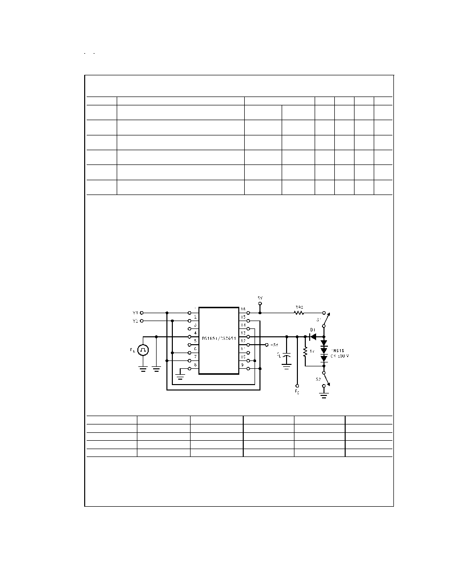
Typical Applications
A Typical MOS Memory Sensing Application for a 4k work by 4-bit
Memory Arrangement Employing 1103 Type Memory Devices
DS007528-2
Note: Only 4 devices are required for a 4k word by 16-bit memory system.
www.national.com
2
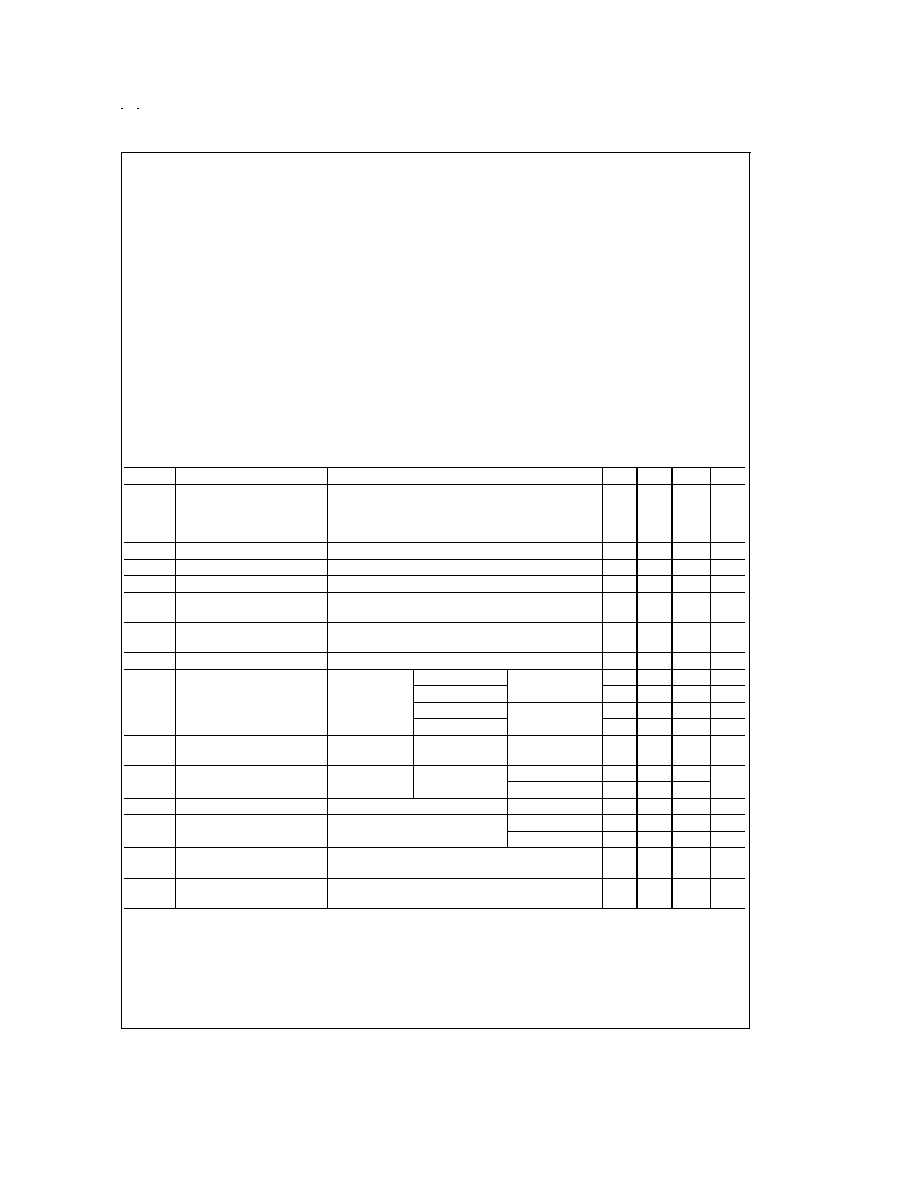
Absolute Maximum Ratings
(Note 2)
If Military/Aerospace specified devices are required,
please contact the National Semiconductor Sales Office/
Distributors for availability and specifications.
Power Supply Voltages
V
CC
V
EE
+7 V
DC
-7 V
DC
Differential-Mode Input Signal Voltage
Range, V
IDR
±
6 V
DC
Common-Mode Input Voltage Range,
V
ICR
±
5 V
DC
Strobe Input Voltage, V
I(S)
5.5 V
DC
Strobe Temperature Range
-65∞C to +150∞C
Maximum Power Dissipation (Note 1) at 25∞C
Cavity Package
Molded Package
1509 mW
1476 mW
Lead Temp. (Soldering, 10 seconds)
300∞C
Operating Conditions
Min
Max
Unit
Supply Voltage (V
CC
)
DS1651
DS3651
4.5
4.75
5.5
5.25
V
V
Supply Voltage (V
EE
)
DS1651
DS3651
-4.5
-4.75
-5.5
-5.25
V
V
Operating Temperature (T
A
)
DS1651
DS3651
-55
0
+125
+70
∞C
∞C
Output Load Current, (I
OL
)
16
mA
Differential Mode Input
Voltage Range, (V
IDR
)
-5.0
+5.0
V
Common-Mode Input
Voltage Range, (V
ICR
)
-3.0
+3.0
V
Input Voltage Range
(Any Input to GND), (V
IR
)
-5.0
+3.0
V
Electrical Characteristics
V
CC
= 5 V
DC
, V
EE
= -5 V
DC
, Min
T
A
Max, unless otherwise noted (Notes 3, 4)
Symbol
Parameter
Conditions
Min
Typ
Max
Unit
V
IS
Input Sensitivity (Note 6)
(Common-Mode Voltage
Range)
V
ICR
= -3V
V
IN
+3V
Min
V
CC
Max
Min
V
EE
Max
±
7.0
mV
V
IO
Input Offset Voltage
2
mV
I
IB
Input Bias Current
V
CC
= Max, V
EE
= Max
20
µA
I
IO
Input Offset Current
0.5
µA
V
IL(S)
Strobe Input Voltage
(Low State)
0.8
V
V
IH(S)
Strobe Input Voltage
(High State)
2
V
I
IL(S)
Strobe Current (Low State)
V
CC
= Max, V
EE
= Max, V
IN
= 0.4V
-1.6
mA
I
IL(S)
Strobe Current (High State)
V
CC
= Max,
V
EE
= Max
V
IN
= 2.4V
DS3651
40
µA
V
IN
= V
CC
1
mA
V
IN
= 2.4V
DS1651
100
µA
V
IN
= V
CC
1
mA
V
OH
Output Voltage (High States)
V
CC
= Min,
V
EE
= Min
I
O
= -400 µA
DS1651/DS3651
2.4
V
V
OL
Output Voltage (Low State)
V
CC
= Min,
V
EE
= Min
I
O
= 16 mA
DS3651
0.45
V
DS1651
0.50
I
OS
Output Current Short Circuit
V
CC
= Max, V
EE
= Max, (Note 5)
DS1651/DS3651
-18
-70
mA
I
OFF
Output Disable Leakage
Current
V
CC
= Max, V
EE
= Max
DS3651
40
µA
DS1651
100
µA
I
CC
High Logic Level Supply
Current
V
CC
= Max, V
EE
= Max
45
60
mA
I
EE
High Logic Level Supply
Current
V
CC
= Max, V
EE
= Max
-17
-30
mA
www.national.com
3
Switching Characteristics
V
CC
= 5 V
DC
, V
EE
= -5 V
DC
, T
A
= 25∞C unless otherwise noted.
Symbol
Parameter
Conditions
Min
Typ
Max
Units
t
PHL(D)
High-to-Low Logic Level Propagation
Delay Time (Differential Inputs)
5 mV + V
IS
,
(
Figure 2)
DS1651/
DS3651
23
45
ns
t
PLH(D)
Low-to-High Logic Level Propagation
Delay Time (Differential Inputs)
5 mV + V
IS
,
(
Figure 2)
DS1651/
DS3651
22
55
ns
t
POH(S)
TRI-STATE to High Logic Level
Propagation Delay Time (Strobe)
(
Figure 1)
DS1651/
DS3651
16
21
ns
t
PHO(S)
High Logic Level to TRI-STATE
Propagation Delay Time (Strobe)
(
Figure 1)
DS1651/
DS3651
7
18
ns
t
POL(S)
TRI-STATE to Low Logic Level
Propagation Delay Time (Strobe)
(
Figure 1)
DS1651/
DS3651
19
27
ns
t
PLO(S)
Low Logic Level to TRI-STATE
Propagation Delay Time (Strobe)
(
Figure 1)
DS1651/
DS3651
14
29
ns
Note 1: Derate cavity package 10.1 mW/∞C above 25∞C; derate molded package 11.8 mW/∞C above 25∞C.
Note 2: "Absolute Maximum Ratings" are those values beyond which the safety of the device cannot be guaranteed. Except for "Operating Temperature Range" they
are not meant to imply that the device should be operated at these limits. The table of "Electrical Characteristics" provides conditions for actual device operation.
Note 3: Unless otherwise specified min/max limits apply across the 0∞C to +70∞C range for the DS3651 and across the -55∞C to +125∞C range for the DS1651. All
typical values are for T
A
= 25∞C, V
CC
= 5V and V
EE
= -5V.
Note 4: All currents into device pins shown as positive, out of device pins as negative, all voltages referenced to ground unless otherwise noted. All values shown
as max or min on absolute value basis.
Note 5: Only one output at a time should be shorted.
Note 6: A parameter which is of primary concern when designing with sense amplifiers is, what is the minimum differential input voltage required at the sense am-
plifier input terminals to guarantee a given output logic state. This parameter is commonly referred to as threshold voltage. It is well known that design considerations
of threshold voltage are plagued by input offset currents, bias currents, network source resistances, and voltage gain. As a design convenience, the DS1651 and
DS3651 are specified to a parameter called input sensitivity (V
IS
). This parameter takes into consideration input offset currents and bias currents, and guarantees
a minimum input differential voltage to cause a given output logic state with respect to a maximum source impedance of 200
at each input.
Switching Time Waveform
Delay
V1
V2
S1
S2
C
L
t
PLO(S)
)
100 mV
GND
Closed
Closed
15 pF
t
POL(S)
100 mV
GND
Closed
Open
50 pF
t
PHO(S)
GND
100 mV
Closed
Closed
15 pF
t
POH(S)
GND
100 mV
Open
Closed
50 pF
C
L
includes jig and probe capacitance.
E
IN
waveform characteristics: t
TLH
and t
THL
10 ns measured 10% to 90%
PRR = 1 MHz
Duty cycle = 50%
DS007528-3
Note: Output of channel B shown under test, other channels are tested similarly.
www.national.com
4
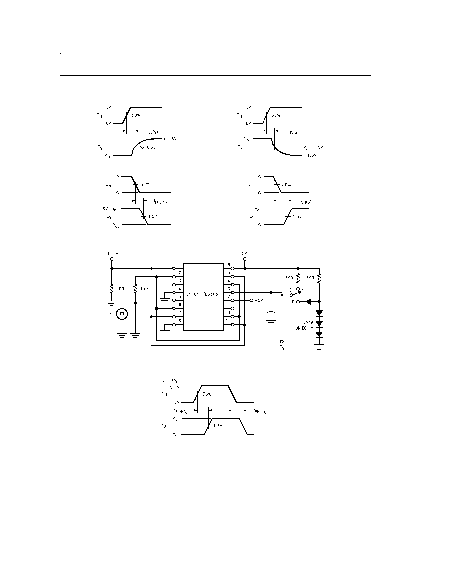
AC Test Circuits
t
PLO(S)
DS007528-4
t
PHO(S)
DS007528-5
t
POL(S)
DS007528-6
t
POH(S)
DS007528-7
FIGURE 1. Strobe Propagation Delay t
PLO(S)
, t
POL(S)
, t
PHL(S)
and t
POH(S)
DS007528-8
Note: Output of channel B shown under test, other channels are tested similarly.
S1 at "B" for DS1651/DS3651, C
L
= 50 pF total for DS1651/DS3651.
DS007528-9
E
IN
waveform characteristics:
t
TLH
and t
THL
10 ns measured 10% to 90%
PRR = 1 MHz, duty cycle = 500 ns
FIGURE 2. Differential Input Propagation Delay t
PLH(D)
and t
PHL(D)
www.national.com
5