 | –≠–ª–µ–∫—Ç—Ä–æ–Ω–Ω—ã–π –∫–æ–º–ø–æ–Ω–µ–Ω—Ç: DS3654N | –°–∫–∞—á–∞—Ç—å:  PDF PDF  ZIP ZIP |
TL F 5817
DS3654
Printer
Solenoid
Driver
August 1992
DS3654 Printer Solenoid Driver
General Description
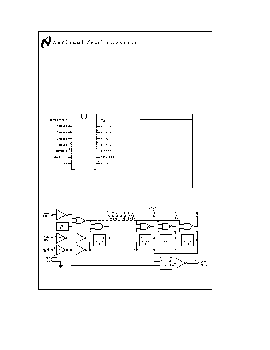
The DS3654 is a serial-to-parallel 10-bit shift register with a
clock and data input a data output from the tenth bit and
10 open-collector clamped relay driver outputs suitable for
driving printer solenoids
Timing for the circuit is shown in
Figure 1 Data input is
sampled on the positive clock edge Data output changes
on the negative clock edge and is always active Enable
transfers data from the shift register to the open-collector
outputs Internal circuitry inhibits output enable for power
supply voltage less than 6V
Each output sinks 250 mA and is internally clamped to
ground at 50V to dissipate energy stored in inductive loads
Connection Diagram
Dual-In-Line Package
TL F 5817 ≠ 1
Top View
Order Number DS3654N
See NS Package Number N16E
Pin Descriptions
Pin No
Function
1
Output Enable
2
Output 6
3
Output 7
4
Output 8
5
Output 9
6
Output 10
7
Data Output
8
Ground
9
Clock Input
10
Data Input
11
Output 1
12
Output 2
13
Output 3
14
Output 4
15
Output 5
16
V
CC
Logic Diagram
TL F 5817 ≠ 2
C1995 National Semiconductor Corporation
RRD-B30M105 Printed in U S A
Absolute Maximum Ratings
(Note 1)
If Military Aerospace specified devices are required
please contact the National Semiconductor Sales
Office Distributors for availability and specifications
Supply Voltage V
CC
9 5V Max
Input Voltage
b
0 5V Min 9 5V Max
Output Supply Vp-p
45V Max
Storage Temperature Range
b
65 C to
a
150 C
Output Current (Single Output)
0 4A
Ground Current
4 0A
Peak Power Dissipation t
k
10 ms
Duty Cycle
k
5%
4 5W Max
Maximum Power Dissipation at 25 C
Molded Package
1687 mW
Lead Temperature (Soldering 4 seconds)
260 C
Derate molded package 13 5 mW C above 25 C
Operating Conditions
Min
Max
Units
Supply Voltage (V
CC
)
7 5
9 5
V
Temperature (T
A
)
0
a
70
C
Output Supply (Vp-p)
40
V
Electrical Characteristics
(Notes 2 3 and 4) Vp-p
e
30V unless otherwise noted
Parameter
Conditions
Min
Typ
Max
Units
Logical ``1'' Input Voltage
2 6
V
Logical ``0'' Input Voltage
0 8
V
Logical ``1'' Output Voltage Clamp
I
CLAMP
e
0 1A V
EN
e
0V
45
50
65
V
Logical ``1'' Output Current
V
OH
e
40V V
EN
e
0V
1 0
mA
Logical ``0'' Output Voltage
I
OL
e
250 mA V
EN
e
2 6V
1 6
V
Logical ``1'' Input Current
Clock
T
A
e
70 C V
CL
e
2 6V
0 2
0 33
mA
Enable
T
A
e
70 C V
EN
e
2 6V
0 2
0 33
mA
Data
T
A
e
70 C V
D
e
2 6V
0 3
0 57
mA
Clock
T
A
e
0 C V
CL
e
2 6V
0 33
0 5
mA
Enable
T
A
e
0 C V
EN
e
2 6V
0 33
0 5
mA
Data
T
A
e
0 C V
D
e
2 6V
0 57
0 75
mA
Logical ``0'' Input Current
Clock
T
A
e
70 C V
CL
e
1V
125
m
A
Enable
T
A
e
70 C V
EN
e
1V
125
m
A
Data
T
A
e
70 C V
D
e
1V
220
m
A
Input Pull-Down Resistance
Clock
T
A
e
25 C V
CL
k
V
CC
8
kX
Enable
T
A
e
25 C V
EN
k
V
CC
8
kX
Data
T
A
e
25 C V
D
k
V
CC
4 5
kX
Supply Current (I
CC
)
Outputs Disabled
T
A
t
25 C V
EN
e
0V V
DO
e
0V
27
40
mA
V
CC
e
9 5V
Outputs Enabled
T
A
t
25 C V
EN
e
2 6V I
OL
e
250 mA
55
70
mA
Each Bit
Data Output Low (V
DOL
)
V
D
e
0V I
OL
e
0V
0 01
0 5
V
Data Output High (V
DOH
)
V
D
e
2 6V I
OH
e b
0 75 mA
2 6
3 4
V
Data Output Pull-Down Resistance
V
D
e
0V V
D0
e
1V
14
kX
Note 1
``Absolute Maximum Ratings'' are those values beyond which the safety of the device cannot be guaranteed They are not meant to imply that the devices
should be operated at these limits The tables of ``Electrical Characteristics'' provide conditions for actual device operation
Note 2
Unless otherwise specified min max limits apply across the 0 C to
a
70 C temperature range and the 7 5V to 9 5V power supply range All typical values
given are for V
CC
e
8 5V and T
A
e
25 C
Note 3
All currents into device pins are positive all currents out of device pins are negative All voltages are referenced to ground unless otherwise specified
Note 4
Only one output at a time should be shorted
2
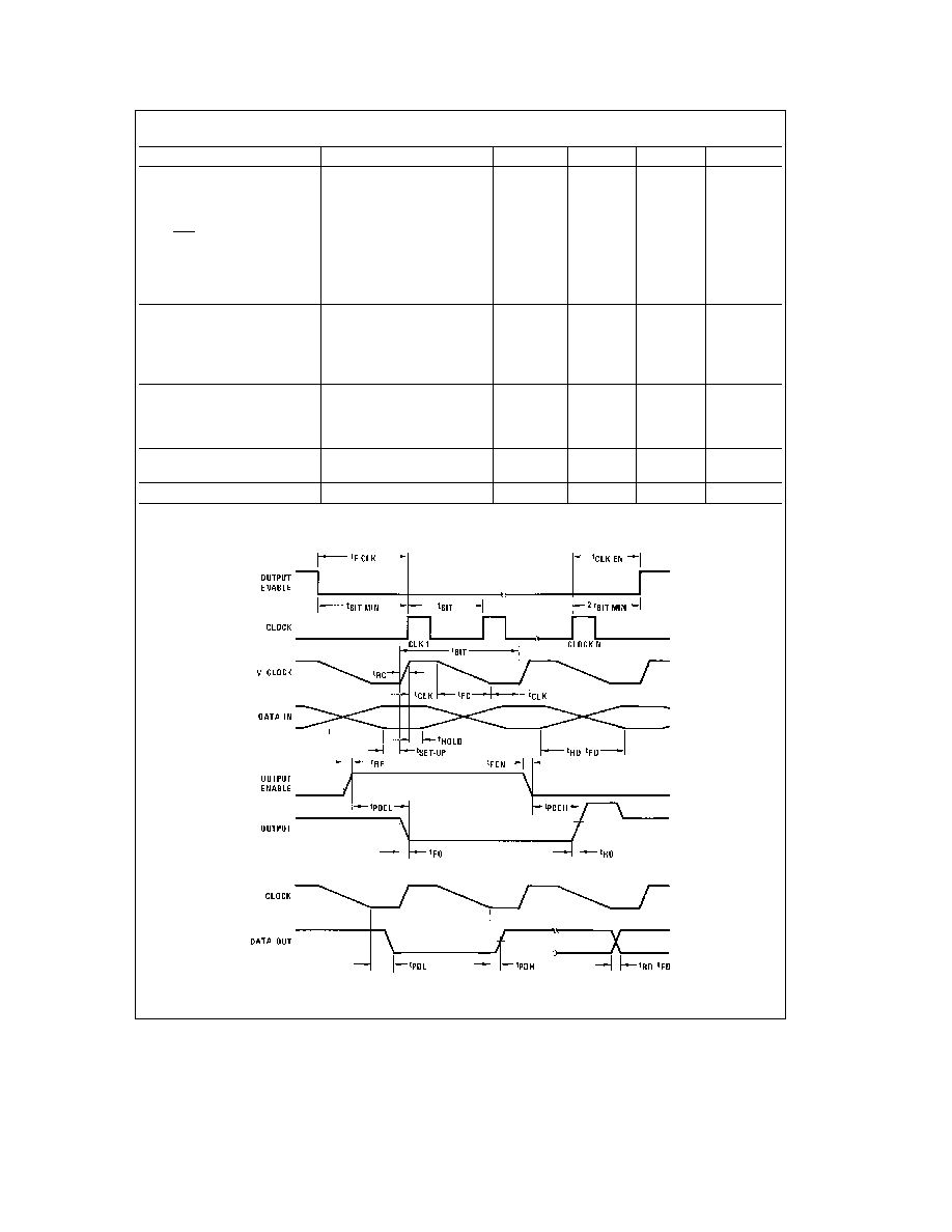
Switching Characteristics
0 C to
a
70 C T
A
e
25 C nominal power supplies unless otherwise noted
Parameter
Conditions
Min
Typ
Max
Units
Clk Data and Enable Inputs
(Figure 1)
t
FC
2 0
m
s
t
RC
t
BIT
t
10 ms
2 0
m
s
t
CLK
2
m
s
t
CLK
3 5
m
s
t
HOLD
1 0
m
s
t
SET-UP
1 0
m
s
t
RE
t
RD IN
1 0
m
s
t
FE
t
FD IN
5 0
m
s
Output 1 ≠ 10
Vp-p
e
20V
t
RO
R
L
e
100X C
L
k
100 pF
1 2
m
s
t
FO
R
L
e
100X C
L
k
100 pF
1 2
m
s
t
PDEH
3 5
m
s
t
PDEL
3 0
m
s
Data Output
t
PDH
t
PDL
R
L
e
5 kX C
L
s
10 pF
0 8
2 5
m
s
t
RD
0 4
m
s
t
FD
0 4
m
s
Clock to Enable Delay
t
CE
2 t
BIT
m
s
Enable to Clock Delay
t
BIT
m
s
Switching Time Waveforms
TL F 5817 ≠ 3
FIGURE 1 Shift Timing
3
DS3654
Printer
Solenoid
Driver
Definition of Terms
Vp-p
Output power supply voltage The return for open-col-
lector relay driver outputs
t
BIT
Period of the incoming clock
V
CLK
The voltage at the clock input
t
CLK
The portion of t
BIT
when V
CLK
t
2 6V
t
CLK
The portion of t
BIT
when V
CLK
s
0 8V
t
SET-UP
The time prior to the end of t
CLK
required to insure
valid data at the shift register input for subsequent clock
transitions
t
HOLD
The time following the start of t
CLK
required to trans-
fer data within the shift register
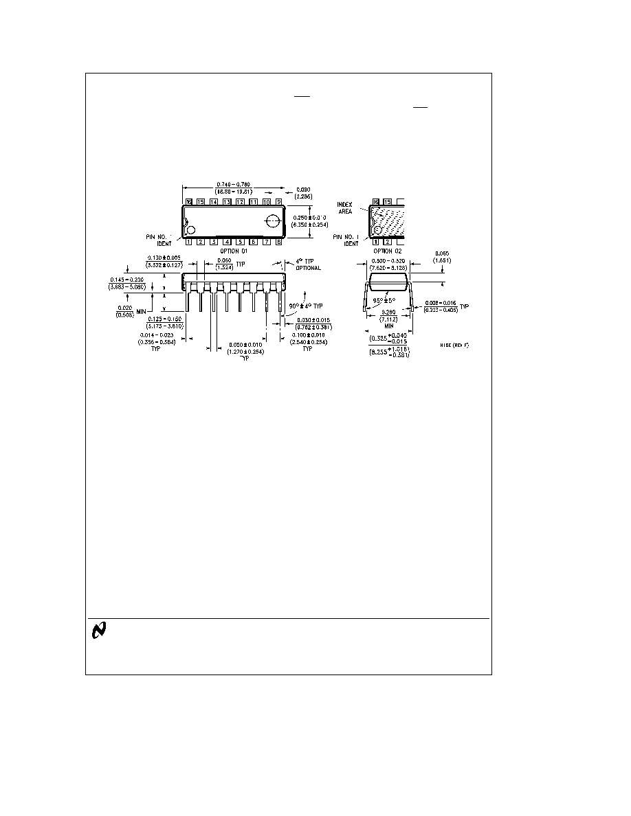
Physical Dimensions
inches (millimeters)
Molded Dual-In-Line Package (N)
Order Number DS3654N
NS Package Number N16E
LIFE SUPPORT POLICY
NATIONAL'S PRODUCTS ARE NOT AUTHORIZED FOR USE AS CRITICAL COMPONENTS IN LIFE SUPPORT
DEVICES OR SYSTEMS WITHOUT THE EXPRESS WRITTEN APPROVAL OF THE PRESIDENT OF NATIONAL
SEMICONDUCTOR CORPORATION As used herein
1 Life support devices or systems are devices or
2 A critical component is any component of a life
systems which (a) are intended for surgical implant
support device or system whose failure to perform can
into the body or (b) support or sustain life and whose
be reasonably expected to cause the failure of the life
failure to perform when properly used in accordance
support device or system or to affect its safety or
with instructions for use provided in the labeling can
effectiveness
be reasonably expected to result in a significant injury
to the user
National Semiconductor
National Semiconductor
National Semiconductor
National Semiconductor
Corporation
Europe
Hong Kong Ltd
Japan Ltd
1111 West Bardin Road
Fax (a49) 0-180-530 85 86
13th Floor Straight Block
Tel 81-043-299-2309
Arlington TX 76017
Email cnjwge tevm2 nsc com
Ocean Centre 5 Canton Rd
Fax 81-043-299-2408
Tel 1(800) 272-9959
Deutsch Tel (a49) 0-180-530 85 85
Tsimshatsui Kowloon
Fax 1(800) 737-7018
English
Tel (a49) 0-180-532 78 32
Hong Kong
Fran ais Tel (a49) 0-180-532 93 58
Tel (852) 2737-1600
Italiano
Tel (a49) 0-180-534 16 80
Fax (852) 2736-9960
National does not assume any responsibility for use of any circuitry described no circuit patent licenses are implied and National reserves the right at any time without notice to change said circuitry and specifications