
TL F 5818
DS3656
Quad
Peripheral
Driver
March 1990
DS3656 Quad Peripheral Driver
General Description
The DS3656 is a quad peripheral driver designed for use in
automotive applications Logically it is an open collector
NAND function with all inputs compatible with 74LS and
CMOS series products An enable input is provided that is
common to each driver When taken to a logic zero level all
outputs will turn off Also overvoltage is detected
The DS3656 has features associated with the output struc-
ture that make it highly versatile to many applications Each
output is capable of 600 mA sink currents and offers 65V
standoff voltage in non-inductive applications A clamp net-
work capable of handling 800 mA is incorporated in each
output which eliminates the need of an external network to
quench the high voltage backswing caused when switching
inductive loads up to 30V (reference AN-213)
The DS3656 is intended to operate from a 12V automotive
battery Internal to the device is its own voltage regulator
which permits the device to operate during the wide voltage
variation seen in many automotive applications An over-
voltage-protection circuit is incorporated that will cause the
outputs to turn off when the supply exceeds 30V The circuit
is designed to withstand worst case fault conditions that
occur in automotive applications such as high voltage tran-
sients and reverse battery connection In this type of envi-
ronment an external 100X resistor must be connected in
series with the V
CC
line
The molded package is specifically constructed to allow in-
creased power dissipation over conventional packages The
four ground pins are directly connected to the device chip
with a special copper lead frame When the quad driver is
soldered into a copper PC board the power rating of the
device will significantly improve
Features
Y
Quad automotive peripheral driver
Y
600 mA output current capability
Y
High voltage outputs
65V
Y
Clamp diode provided for inductive loads
Y
Built in regulator
Y
Overvoltage failsafe
Y
TTL LS CMOS compatible diode clamped inputs
Y
High power dissipation package
Y
Guaranteed to withstand worst case fault conditions
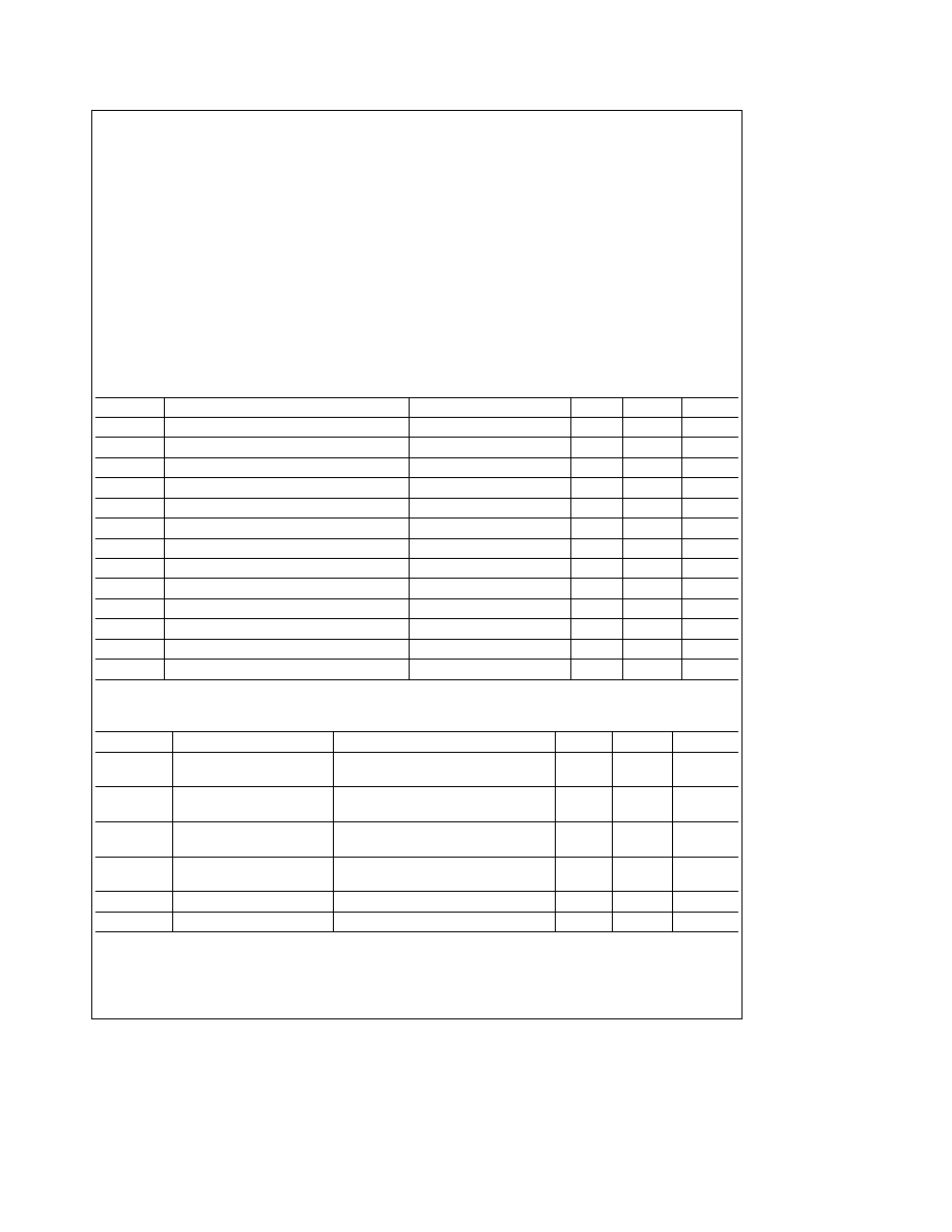
Connection Diagram
Dual-In-Line Package
TL F 5818 � 1
Top View
Order Number DS3656N
See NS Package Number N16A
Truth Table
Enable
In X
Out X
H
H
L
H
L
Z
L
X
Z
H
e
High level
L
e
Low level
X
e
Irrelevant
Z
e
High impedance state
C1995 National Semiconductor Corporation
RRD-B30M105 Printed in U S A
Absolute Maximum Ratings
(Note 1)
If Military Aerospace specified devices are required
please contact the National Semiconductor Sales
Office Distributors for availability and specifications
Supply Voltage V
CC
(Note 2)
65V
Input Voltage
7V
Output Voltage
65V
Continuous Output Current
1 2A
Junction Temperature
150 C
Thermal Resistance (Junction to Ambient)
DS3656N Plugged in a Socket
60 C W
DS3656N Soldered in a PC Board
35 C W
DS3656N Soldered in a PC Board
with 6 in
2
Cn Foil
20 C W
Lead Temperature (Soldering 4 seconds)
260 C
Operating Conditions
Min
Max
Units
Supply Voltage V
CC
10 5
17 0
V
Temperature
b
40
105
C
Electrical Characteristics
(Notes 2 and 3)
Symbol
Parameter
Conditions
Min
Max
Units
V
CC
Power Supply Voltage
10 5
17
V
I
CC
Power Supply Current
65
mA
V
IH
High Level Input Voltage
2 0
V
V
IL
Low Level Input Voltage
0 8
V
I
IH
High Level Input Current
V
IN
e
2 7V
20
m
A
I
IL
Low Level Input Current
V
IN
e
0 4V
b
360
m
A
V
ICL
Input Clamp Voltage
I
IN
e b
10 mA
b
1 5
V
V
OL
Low Level Output Voltage
I
L
e
600 mA V
CC
e
10 5V
1 5
V
I
OH
High Level Leakage Current
V
OH
e
65V
1 0
mA
V
F
Output Diode Forward Voltage
I
F
e
800 mA
2 5
V
I
R
Output Diode Reverse Leakage
V
R
e
65V
1 0
mA
B
VCER
V
OH1
Switching Capacitive or Resistive Load
65
V
L
VCEO
V
OH2
Switching Inductive Clamped Load
30
V
Switching Characteristics
V
CC
e
13 2V T
A
e
25 C
Symbol
Parameter
Conditions
Min
Max
Units
t
PLH
Propagation Delay Time
V
CC
e
13 2V R
L
e
30X C
L
e
15 pF
10
m
s
Low to High Level Output
t
PHL
Propagation Delay Time
V
CC
e
13 2V R
L
e
30X C
L
e
15 pF
10
m
s
High to Low Level Output
t
TLH
Transition Time
V
CC
e
13 2V R
L
e
30X C
L
e
15 pF
500
ns
Low to High Level Output
t
THL
Transition Time
V
CC
e
13 2V R
L
e
30X C
L
e
15 pF
500
ns
High to Low Level Output
t
PLH
Enable to Output
V
CC
e
13 2V R
L
e
30X C
L
e
15 pF
10
m
s
t
PHL
Enable to Output
V
CC
e
13 2V R
L
e
30X C
L
e
15 pF
10
m
s
Note 1
``Absolute Maximum Ratings'' are those values beyond which the safety of the device cannot be guaranteed Except for ``Operating Temperature Range''
they are not meant to imply that the devices should be operated at these limits The table of ``Electrical Characteristics'' provides conditions for actual device
operation
Note 2
Voltage values are with respect to network ground terminal unless otherwise specified
Note 3
Unless otherwise specified min max limits apply across the
b
40 C to
a
105 C temperature range
2

3
DS3656
Quad
Peripheral
Driver
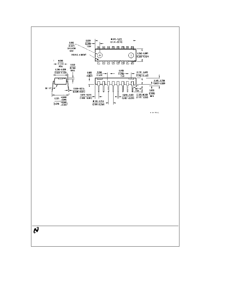
Physical Dimensions
inches (millimeters)
Molded Dual-In-Line Package (N)
Order Number DS3656N
NS Package Number N16A
LIFE SUPPORT POLICY
NATIONAL'S PRODUCTS ARE NOT AUTHORIZED FOR USE AS CRITICAL COMPONENTS IN LIFE SUPPORT
DEVICES OR SYSTEMS WITHOUT THE EXPRESS WRITTEN APPROVAL OF THE PRESIDENT OF NATIONAL
SEMICONDUCTOR CORPORATION As used herein
1 Life support devices or systems are devices or
2 A critical component is any component of a life
systems which (a) are intended for surgical implant
support device or system whose failure to perform can
into the body or (b) support or sustain life and whose
be reasonably expected to cause the failure of the life
failure to perform when properly used in accordance
support device or system or to affect its safety or
with instructions for use provided in the labeling can
effectiveness
be reasonably expected to result in a significant injury
to the user
National Semiconductor
National Semiconductor
National Semiconductor
National Semiconductor
Corporation
Europe
Hong Kong Ltd
Japan Ltd
1111 West Bardin Road
Fax (a49) 0-180-530 85 86
13th Floor Straight Block
Tel 81-043-299-2309
Arlington TX 76017
Email cnjwge tevm2 nsc com
Ocean Centre 5 Canton Rd
Fax 81-043-299-2408
Tel 1(800) 272-9959
Deutsch Tel (a49) 0-180-530 85 85
Tsimshatsui Kowloon
Fax 1(800) 737-7018
English
Tel (a49) 0-180-532 78 32
Hong Kong
Fran ais Tel (a49) 0-180-532 93 58
Tel (852) 2737-1600
Italiano
Tel (a49) 0-180-534 16 80
Fax (852) 2736-9960
National does not assume any responsibility for use of any circuitry described no circuit patent licenses are implied and National reserves the right at any time without notice to change said circuitry and specifications