 | –≠–ª–µ–∫—Ç—Ä–æ–Ω–Ω—ã–π –∫–æ–º–ø–æ–Ω–µ–Ω—Ç: DS3667N | –°–∫–∞—á–∞—Ç—å:  PDF PDF  ZIP ZIP |
TL F 5245
DS3667
TRI-STATE
Bidirectional
Transceiver
February 1996
DS3667 TRI-STATE
Bidirectional Transceiver
General Description
The DS3667 is a high-speed Schottky 8-channel bidirection-
al transceiver designed for digital information and communi-
cation systems Pin selectable totem-pole open collector
outputs are provided at all driver outputs This feature to-
gether with the Dumb Mode which puts both driver and re-
ceiver outputs in TRI-STATE at the same time means high-
er flexibility of system design PNP inputs are used at all
driver inputs for minimum loading and hysteresis is provid-
ed at all receiver inputs for added noise margin A power
up down protection circuit is included at all outputs to pro-
vide glitch-free operation during V
CC
power up or down
Features
Y
8-channel bidirectional non-inverting transceivers
Y
Bidirectional control implemented with TRI-STATE
output design
Y
High speed Schottky design
Y
Low power consumption
Y
High impedance PNP inputs (drivers)
Y
Pin selectable totem-pole open collector outputs
(drivers)
Y
500 mV (typ) input hysteresis (receivers)
Y
Power up down protection (glitch-free)
Y
Dumb Mode capability
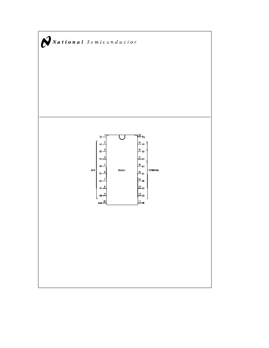
Connection Diagram
Dual-In-Line Package
TL F 5245 ≠ 1
Top View
Order Number DS3667N
See NS Package Number N20A
TRI-STATE
is a registered trademark of National Semiconductor Corp
C1996 National Semiconductor Corporation
RRD-B30M36 Printed in U S A
http
www national com

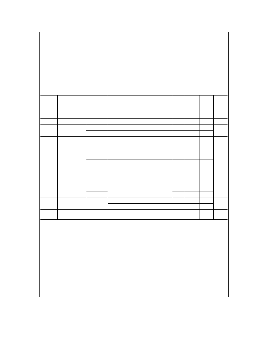
Logic Diagram
TL F 5245 ≠ 2
Functional Truth Table
Control
Input
Data Transceivers
Level
TE
PE
Mode
Bus Port
Terminal Port
H
H
T
Totem-Pole
Input
Output
H
L
T
Open
Input
Collector
Output
L
H
R
Input
Output
L
L
D
TRI-STATE
TRI-STATE
H High Level Input
L Low Level Input
T Transmitting Mode
R Receiving Mode
D Dumb Mode
http
www national com
2
Absolute Maximum Ratings
(Note 1)
If Military Aerospace specified devices are required
please contact the National Semiconductor Sales
Office Distributors for availability and specifications
Supply Voltage (V
CC
)
7 0V
Input Voltage
5 5V
Storage Temperature Range
b
65 C to
a
150 C
Maximum Power Dissipation at 25 C
Molded Package
1832 mW
Lead Temperature (Soldering 4 seconds)
260 C
Derate molded package 14 7 mW C above 25 C
Operating Conditions
Min
Max
Units
V
CC
Supply Voltage
4 75
5 25
V
T
A
Ambient Temperature
0
70
C
I
OL
Output Low Current
Bus
48
mA
Terminal
16
mA
Electrical Characteristics
(Notes 2 and 3)
Symbol
Parameter
Conditions
Min
Typ
Max
Units
V
IH
High Level Input Voltage
2
V
V
IL
Low Level Input Voltage
0 8
V
V
IK
Input Clamp Voltage
I
I
e b
18 mA
b
0 8
b
1 5
V
V
HYS
Input Hysteresis
Bus
400
500
mV
V
OH
High Level
Terminal
I
OH
e b
800 mA
2 7
3 5
V
Output Voltage
Bus
I
OH
e b
5 2 mA
2 5
3 4
V
OL
Low Level
Terminal
I
OL
e
16 mA
0 3
0 5
V
Output Voltage
Bus
I
OL
e
48 mA
0 4
0 5
I
IH
High Level
TE PE
V
I
e
5 5V
0 2
100
Input Current
V
I
e
2 7V
0 1
20
m
A
Terminal
V
I
e
4V
200
and Bus
I
IL
Low Level
Terminal
V
I
e
0 5V
b
10
b
100
m
A
Input Current
and TE PE
Bus
b
0 4
b
1 0
mA
I
OS
Short Circuit
Terminal
V
I
e
2V V
O
e
0V (Note 4)
b
15
b
35
b
75
mA
Output Current
Bus
b
50
b
120
b
200
I
CC
Supply Current
Transmit TE
e
2V PE
e
2V V
I
e
0 8V
75
100
mA
Receive TE
e
0 8V PE
e
2V V
I
e
0 8V
65
90
C
IN
Bus-Port
Bus
V
CC
e
0V V
I
e
0V
20
30
pF
Capacitance
f
e
10 kHz (Note 5)
Note 1
``Absolute Maximum Ratings'' are those values beyond which the safety of the device cannot be guaranteed They are not meant to imply that the device
should be operated at these limits The table of ``Electrical Characteristics'' provides conditions for actual device operations
Note 2
Unless otherwise specified min max limits apply across the 0 C to
a
70 C temperature range and the 4 75V to 5 25V power supply range All typical
values are for T
A
e
25 C and V
CC
e
5 0V
Note 3
All currents into device pins are shown as positive all currents out of device pins are shown as negative all voltages are referenced to ground unless
otherwise specified All values shown as max or min are so classified on absolute value basis
Note 4
Only one output at a time should be shorted
Note 5
This parameter is guaranteed by design It is not a tested parameter
http
www national com
3
Switching Characteristics
V
CC
e
5 0V
g
5% T
A
e
0 C to
a
70 C (Note 1)
Symbol
Parameter
From
To
Conditions
Min
Typ
Max
Units
t
PLH
Propagation Delay Time
V
L
e
2 3V
10
20
ns
Low to High Level Output
Terminal
Bus
R
L
e
38 3X
t
PHL
Propagation Delay Time
C
L
e
30 pF
14
20
ns
High to Low Level Output
(Figure 1)
t
PLH
Propagation Delay Time
V
L
e
5 0V
15
20
ns
Low to High Level Output
Bus
Terminal
R
L
e
240X
t
PHL
Propagation Delay Time
C
L
e
30 pF
10
20
ns
High to Low Level Output
(Figure 2)
t
PZH
Output Enable Time
V
I
e
3 0V
19
30
ns
to High Level
V
L
e
0V
R
L
e
480X
t
PHZ
Output Disable Time
15
20
ns
C
L
e
15 pF
to High Level
TE
Bus
(Figure 1)
t
PZL
Output Enable Time
(Notes 2 and 3)
V
I
e
0V
24
40
ns
to Low Level
V
L
e
2 3V
R
L
e
38 3X
t
PLZ
Output Disable Time
17
30
ns
C
L
e
15 pF
to Low Level
(Figure 1)
t
PZH
Output Enable Time
V
I
e
3 0V
19
35
ns
to High Level
V
L
e
0V
R
L
e
3 kX
t
PHZ
Output Disable Time
17
25
ns
C
L
e
15 pF
to High Level
TE PE
Terminal
(Figure 1)
t
PZL
Output Enable Time
(Notes 2 and 3)
V
I
e
0V
27
40
ns
to Low Level
V
L
e
5V
R
L
e
280X
t
PLZ
Output Disable Time
17
30
ns
C
L
e
15 pF
to Low Level
(Figure 1)
t
PZH
Output Pull-Up Enable
V
I
e
3V
10
20
ns
Time
PE
Bus
V
L
e
0V
R
L
e
480X
t
PHZ
Output Pull-Up Disable
(Notes 2 and 3)
10
20
ns
C
L
e
15 pF
Time
(Figure 1)
Note 1
All typical values are for T
A
e
25 C V
CC
e
5V
Note 2
Refer to Functional Truth Table for control input definition
Note 3
Test configuration should be connected to only one transceiver at a time due to the high current stress caused by the V
I
voltage source when the
output connected to that input becomes active
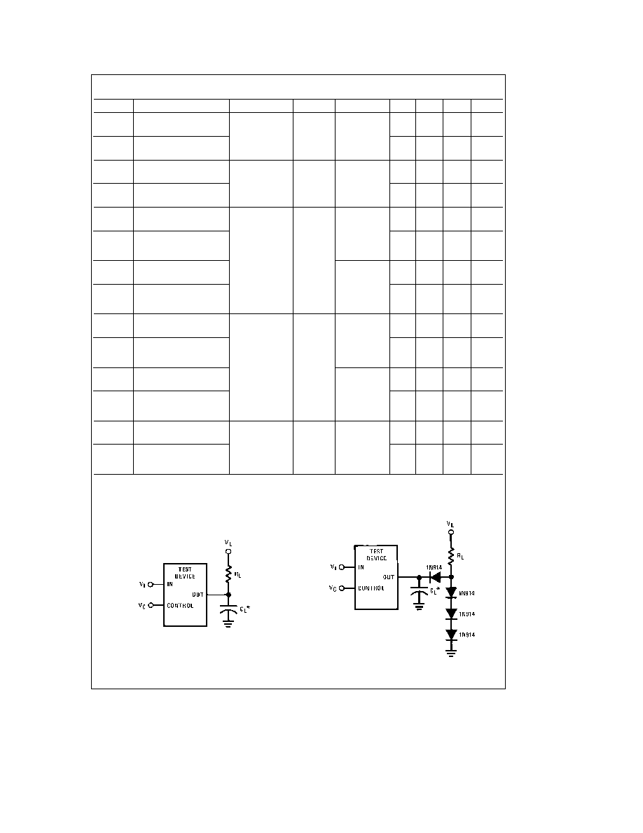
Switching Load Configurations
TL F 5245 ≠ 3
V
C
logic high
e
3 0V
V
C
logic low
e
0V
C
L
includes jig and probe capacitance
FIGURE 1
V
C
logic high
e
3 0V
V
C
logic low
e
0V
TL F 5245 ≠ 4
C
L
includes jig and probe capacitance
FIGURE 2
http
www national com
4
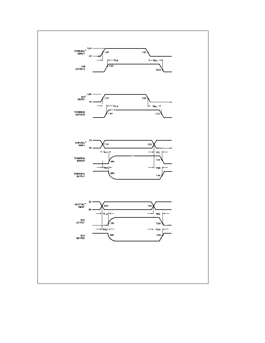
Switching Waveforms
Transmit Propagation Delays
TL F 5245 ≠ 5
Receive Propagation Delays
TL F 5245 ≠ 6
Terminal Enable Disable Times
TL F 5245 ≠ 7
Bus Enable Disable Times
TL F 5245 ≠ 8
Input signal f
e
1 0 MHz 50% duty cycle t
r
e
t
f
s
5 ns
http
www national com
5