TL F 5821
DS3680
Quad
Negative
Voltage
Relay
Driver
March 1995
DS3680 Quad Negative Voltage Relay Driver
General Description
The DS3680 is a quad high voltage negative relay driver
designed to operate over wide ranges of supply voltage
common-mode voltage
and ambient temperature
with
50 mA sink capability These drivers are intended for switch-
ing the ground end of loads which are directly connected to
the negative supply such as in telephone relay systems
Since there may be considerable noise and IR drop be-
tween logic ground and negative supply ground in many ap-
plications these drivers are designed to operate with a high
common-mode range (
g
20V referenced to negative supply
ground) Each driver has a common-mode range separate
from the other drivers in the package which pemits input
signals from more than one element of the system
With low differential input current requirements (typically
100 mA) these drivers are compatible with TTL LS and
CMOS logic Differential inputs permit either inverting or
non-inverting operation
The driver outputs incorporate transient suppression clamp
networks which eliminate the need for external networks
when used in applications of switching inductive loads A
fail-safe feature is incorporated to insure that if the
a
IN
input or both inputs are open the driver will be OFF
Features
Y
b
10V to
b
60V operation
Y
Quad 50 mA sink capability
Y
TTL LS COMS or voltage comparator input
Y
High input common-mode voltage range
Y
Very low input current
Y
Fail-safe disconnect feature
Y
Built-in output clamp diode
Connection Diagram
Dual-In-Line Package
TL F 5821 ≠ 1
Top View
Order Number DS3680J DS3680M or DS3680N
See NS Package Number J14A M14A N14A
Logic Diagram
TL F 5821 ≠ 2
Truth Table
Differential Inputs
Outputs
V
ID
t
2V
On
V
ID
s
0 8V
Off
Open
Off
C1995 National Semiconductor Corporation
RRD-B30M105 Printed in U S A
Absolute Maximum Ratings
(Note 1)
If Military Aerospace specified devices are required
please contact the National Semiconductor Sales
Office Distributors for availability and specifications
Supply Voltage (GND to V
EE
b
and Any Pin)
b
70V
Positive Input Voltage (Input to GND)
20V
Negative Input Voltage (Input to V
EE
b
)
b
5V
Differential Voltage (
a
IN to
b
IN)
g
20V
Inductive Load
L
L
s
5h
I
L
s
50 mA
Output Current
b
100 mA
Storage Temperature
b
65 C to
a
150 C
Maximum Power Dissipation at 25 C
Cavity Package
1433 mW
Molded Dip Package
1398 mW
SO Package
1002 mW
Lead Temperature (Soldering 4 seconds)
260 C
Derate cavity package 9 6 mW C above 25 C derate molded dip pack-
age 11 2 mW C above 25 C derate SO package 8 02 mW C above
25 C
Recommended Operating
Conditions
Min
Max
Units
Supply Voltage (GND to V
EE
b
)
b
10
b
60
V
Input Voltage (Input to GND)
b
20
20
V
Logic ON Voltage (
a
IN)
Referenced to
b
IN
2
20
V
Logic OFF Voltage (
a
IN)
Referenced to
b
IN
b
20
0 8
V
Temperature Range
b
25
a
85
C
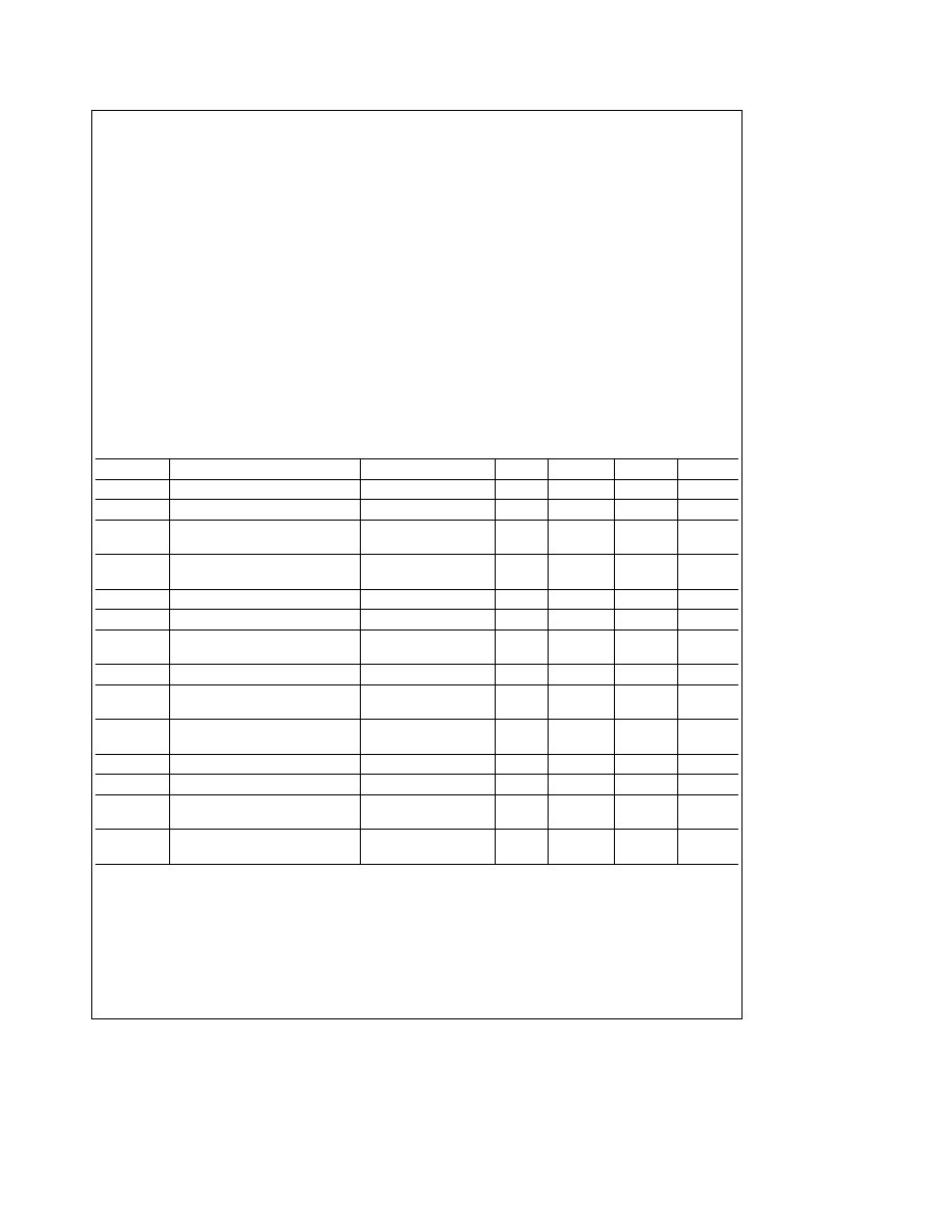
Electrical Characteristics
(Notes 2 and 3)
Symbol
Parameter
Conditions
Min
Typ
Max
Units
V
IH
Logic ``1'' Input Voltage
2 0
1 3
V
V
IL
Logic ``0'' Input Voltage
1 3
0 8
V
I
INH
Logic ``1'' Input Current
V
IN
e
2V
40
100
m
A
V
IN
e
7V
375
1000
m
A
I
INL
Logic ``0'' Input Current
V
IN
e
0 4V
b
0 01
b
5
m
A
V
IN
e b
7V
b
1
b
100
m
A
V
OL
Output ON Voltage
I
OL
e
50 mA
b
1 6
b
2 1
V
I
OFF
Output Leakage
V
OUT
e
V
EE
b
b
2
b
100
m
A
I
FS
Fail-Safe Output Leakage
V
OUT
e
V
EE
b
b
2
b
100
m
A
(Inputs Open)
I
LC
Output Clamp Leakage Current
V
OUT
e
GND
2
100
m
A
V
C
Output Clamp Voltage
I
CLAMP
e b
50 mA
b
2
b
1 2
V
Referenced to V
EE
b
V
P
Positive Output Clamp Voltage
I
CLAMP
e
50 mA
0 9
1 2
V
Referenced to GND
I
EE(ON)
ON Supply Current
All Drivers ON
b
2
b
4 4
mA
I
EE(OFF)
OFF Supply Current
All Drivers OFF
b
1
b
100
m
A
t
PD(ON)
Propagation Delay to Driver ON
L
e
1h R
L
e
1k
1
10
m
s
V
IN
e
3V Pulse
t
PD(OFF)
Propagation Delay to Driver OFF
L
e
1h R
L
e
1k
1
10
m
s
V
IN
e
3V Pulse
Note 1
``Absolute Maximum Ratings'' are those values beyond which the safety of the device cannot be guaranteed Except for ``Operating Temperature Range''
they are not meant to imply that the device should be operated at these limits The table of ``Electrical Characteristics'' provides conditions for actual device
operation
Note 2
Unless otherwise specified the min max limits of the table of ``Electrical Characteristics'' apply within the range of the table of ``Operating Conditions'' All
typical values are given for V
EE
b
e
52V and T
A
e
25 C
Note 3
All current into device pins shown as positive out of the device as negative All voltages are referenced to ground unless otherwise noted
2