TL F 5822
DS3686
Dual
Positive
Voltage
Relay
Driver
April 1990
DS3686 Dual Positive Voltage Relay Driver
General Description
The DS3686 is a high voltage current positive voltage relay
driver having many features not available in present relay
drivers
PNP inputs provide both TTL LS compatibility and high in-
put impedance for low input loading
Output leakage is specified over temperature at an output
voltage of 54V Minimum output breakdown (ac latch break-
down) is specified over temperature at 5 mA This clearly
defines the actual breakdown of the device since the circuit
has incorporated in it an internal reference which does not
allow output breakdown latching found in existing relay driv-
ers Additionally this internal reference circuit feature will
eliminate the need in most cases of an external clamping
(inductive transient voltage protection) diode When the out-
put is turned ``OFF'' by input logic conditions the resulting
inductive voltage transient seen at the output is detected by
an internal zener reference The reference then momentari-
ly activates the output transistor long enough so that the
relay energy is discharged This feature eliminates the need
of external circuit protection components and insures output
transistor protection
The outputs are Darlington connected transistors which al-
low high current operation at low internal V
CC
current
levels
base drive for the output transistor is obtained from
the load in proportion to the required loading conditions
Typical V
CC
power with both outputs ``ON'' is 90 mW
The circuit also features output transistor protection if the
V
CC
supply is lost by forcing the output into the high imped-
ance ``OFF'' state with the same breakdown levels as when
V
CC
was applied
Features
Y
TTL LS CMOS compatible inputs
Y
High impedance inputs (PNP's)
Y
High output voltage breakdown (65V typ)
Y
High output current capability (300 mA max)
Y
Internal protection circuit eliminates need for output
protection diode
Y
Output breakdown protection if V
CC
supply is lost
Y
Low V
CC
power dissipation (90 mW (typ) both outputs
``ON'')
Y
Voltage and current levels compatible for use in tele-
phone relay applications
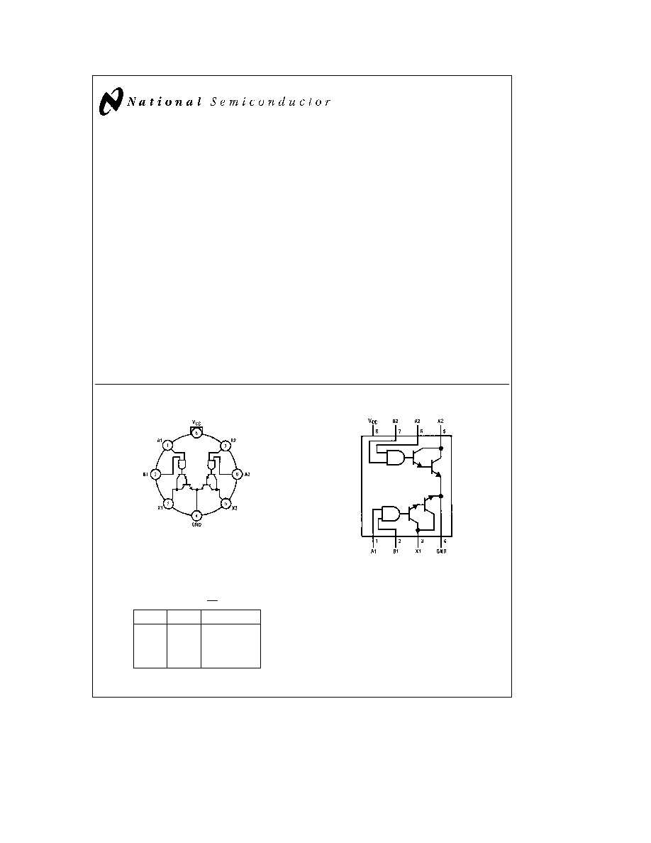
Connection Diagrams
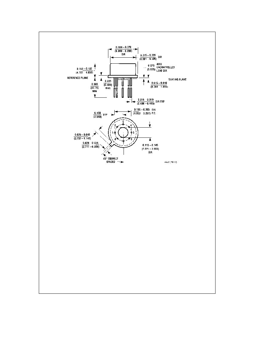
Metal Can Package
TL F 5822 ≠ 1
Top View
Pin 4 is in electrical contact with the case
Order Number DS3686H
See NS Package Number H08C
Truth Table
Positive logic AB
e
X
A
B
Output X
0
0
1
1
0
1
0
1
1
1
1
0
Logic ``0'' output ``ON''
Logic ``1'' output ``OFF''
Dual-In-Line Package
TL F 5822 ≠ 2
Top View
Order Number DS3686J-8 or DS3686N
See NS Package Number J08A or N08E
C1995 National Semiconductor Corporation
RRD-B30M105 Printed in U S A

Absolute Maximum Ratings
(Note 1)
If Military Aerospace specified devices are required
please contact the National Semiconductor Sales
Office Distributors for availability and specifications
Supply Voltage
7V
Input Voltage
15V
Output Voltage
56V
Storage Temperature Range
b
65 C to
a
150 C
Maximum Power Dissipation at 25 C
Cavity Package
1133 mW
Molded Package
1022 mW
TO-5 Package
787 mW
Lead Temperature (Soldering 4 seconds)
260 C
Derate cavity package 7 6 mW C above 25 C derate molded package 8 2
mW C above 25 C derate TO-5 package 5 2 mW C above 25 C
Operating Conditions
Min
Max
Units
Supply Voltage V
CC
4 75
5 25
V
Temperature T
A
0
g
70
C
Electrical Characteristics
(Notes 2 and 3)
Symbol
Parameter
Conditions
Min
Typ
Max
Units
V
IH
Logical ``1'' Input Voltage
R
L
e
180X V
L
e
54V V
O
s
2 5V
2 0
V
I
IH
Logical ``1'' Input Current
V
CC
e
Max V
IN
e
5 5V
0 01
40
m
A
V
IL
Logical ``0'' Input Voltage
R
L
e
180X V
L
e
54V V
O
s
53 8V
0 8
V
I
IL
Logical ``0'' Input Current
V
CC
e
Max V
IN
e
0 4V
b
150
b
250
m
A
V
CD
Input Clamp Voltage
V
CC
e
5V I
CLAMP
e b
12 mA T
A
e
25 C
b
1 0
b
1 5
V
V
OH
Output Breakdown
V
CC
e
Max V
IN
e
0V I
OUT
e
5 mA
56
65
V
I
OH
Output Leakage
V
CC
e
Max V
IN
e
0 4V V
OUT
e
54V
0 5
250
m
A
V
OL
Output ON Voltage
V
CC
e
Min
DS3686
I
OL
e
100 mA
0 85
1 0
V
V
IN
e
2 4V
I
OL
e
300 mA
1 0
1 2
V
I
CC(1)
Supply Current (Both Drivers)
V
CC
e
Max V
IN
e
0V Outputs Open
2
4
mA
I
CC(0)
Supply Current (Both Drivers)
V
CC
e
Max V
IN
e
3V Outputs Open
18
28
mA
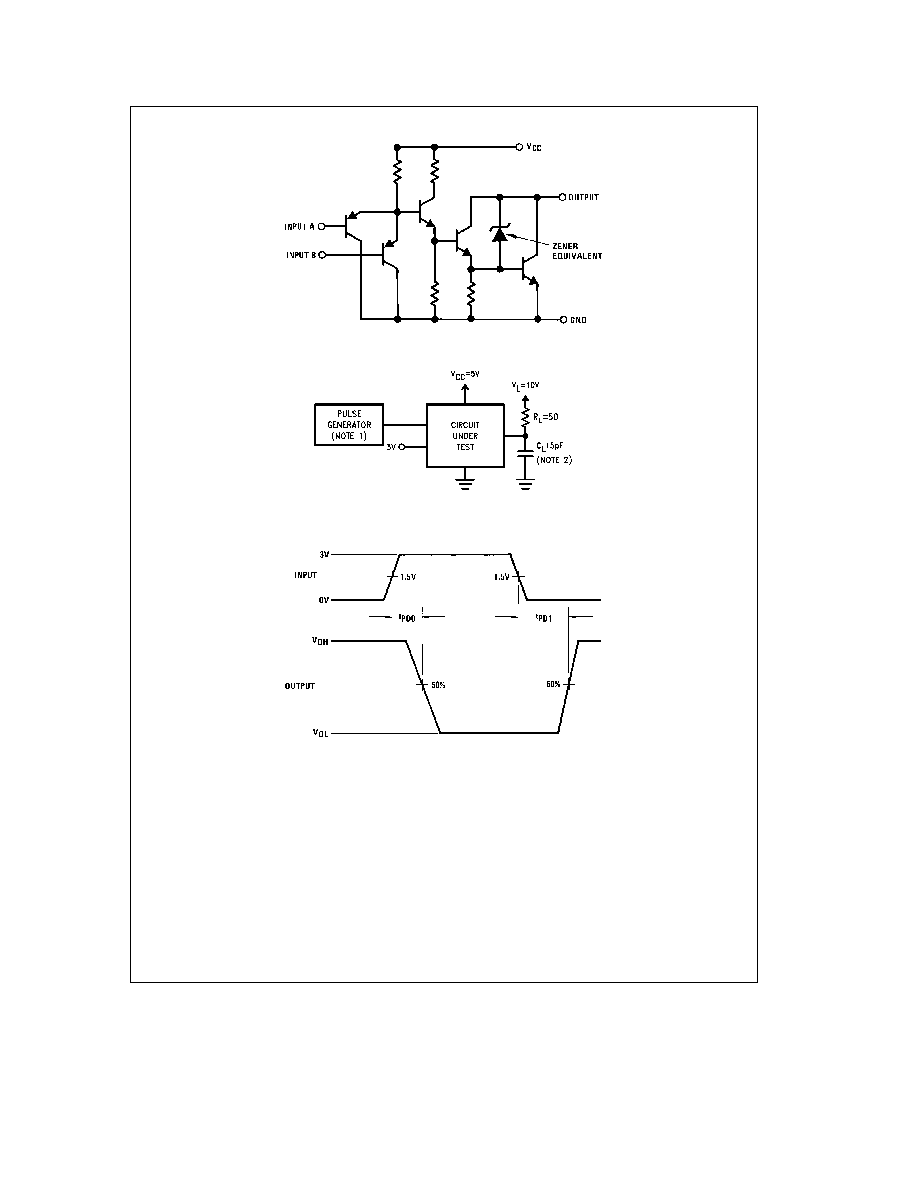
t
PD0
Propagation Delay to a Logical ``0''
C
L
e
15 pF V
L
e
10V R
L
e
50X
50
ns
(Output Turn ON)
T
A
e
25 C V
CC
e
5V
t
PD1
Propagation Delay to a Logical ``1''
C
L
e
15 pF V
L
e
10V R
L
e
50X
1
m
s
(Output Turn OFF)
T
A
e
25 C V
CC
e
5V
Note 1
``Absolute Maximum Ratings'' are those values beyond which the safety of the device cannot be guaranteed Except for ``Operating Temperature Range''
they are not meant to imply that the devices should be operated at these limits The table of ``Electrical Characteristics'' provides conditions for actual device
operation
Note 2
Unless otherwise specified min max limits apply across the 0 C to
a
70 C range for the DS3686 All typicals are given for V
CC
e
5V and T
A
e
25 C
Note 3
All currents into device pins shown as positive out of device pins as negative all voltages referenced to ground unless otherwise noted All values shown
as max or min on absolute value basis
2