 | ÐлекÑÑоннÑй компоненÑ: DS3692J | СкаÑаÑÑ:  PDF PDF  ZIP ZIP |
Äîêóìåíòàöèÿ è îïèñàíèÿ www.docs.chipfind.ru
DS1692/DS3692
TRI-STATE
®
Differential Line Drivers
General Description
The DS1692/DS3692 are low power Schottky TTL line driv-
ers electrically similar to the DS1691A/DS3691 but tested to
meet the requirements of MIL-STD-188-114A (see Applica-
tion Note AN-216). MIL-STD-188-114A type 1 driver specifi-
cations can be met by adding an external three resistor volt-
age divider to the output of the DS3692/1692. The DS3692/
1692 feature 4 buffered outputs with high source and sink
current capability with internal short circuit protection.
With the mode select pin low, the DS1692/DS3692 are dual
differential line drivers with TRI-STATE outputs. They feature
±
10V output common-mode range in TRI-STATE and 0V
output unbalance when operated with
±
5V supply.
Multipoint applications in differential mode with waveshaping
capacitors is not allowed.
Features
n
Short circuit protection for both source and sink outputs
n
100
transmission line drive capability
n
Low I
CC
and I
EE
power consumption:
Differential
mode:
I
CC
= 9 mA/driver typ, I
EE
= 5 mA/driver typ
n
Low current PNP inputs compatible with TTL, MOS and
CMOS
n
Adaptable as MIL-STD-188-114A type 1 driver
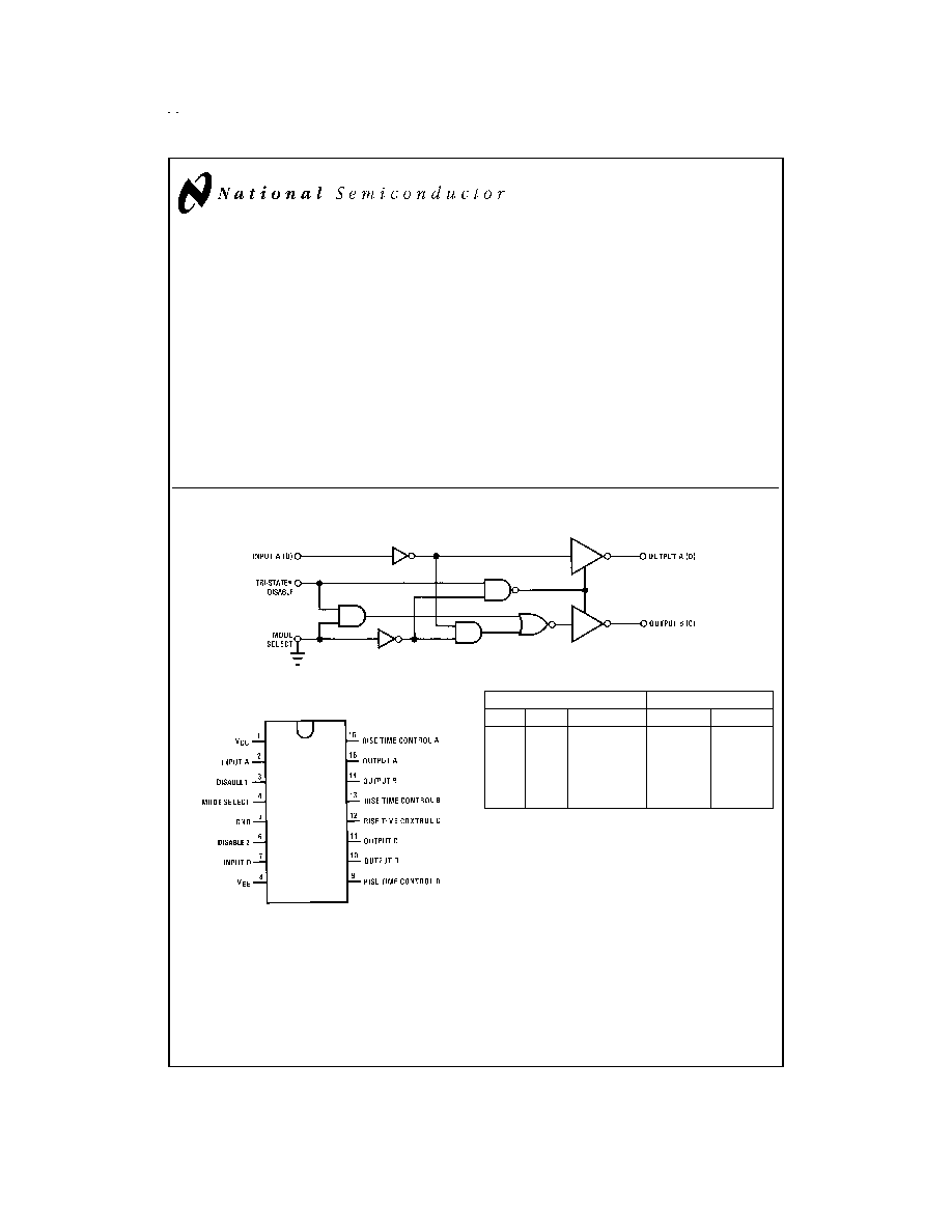
Logic Diagram (
1
/
2
Circuit Shown)
Connection Diagram
Inputs
Outputs
Mode
A (D)
Disable1 (2)
A (D)
B (C)
0
0
0
0
1
0
0
1
TRI-STATE TRI-STATE
0
1
0
1
0
0
1
1
TRI-STATE TRI-STATE
TRI-STATE
®
is a registered trademark of National Semiconductor Corporation.
DS005784-1
DS005784-2
*Contact Product Marketing for availability.
Top View
Order Number DS1692J, DS3692J,
DS3692M or DS3692N
See NS Package Number J16A, M16A
*
or N16A
March 1992
DS1692/DS3692
TRI-ST
A
T
E
Differential
Line
Drivers
© 1999 National Semiconductor Corporation
DS005784
www.national.com
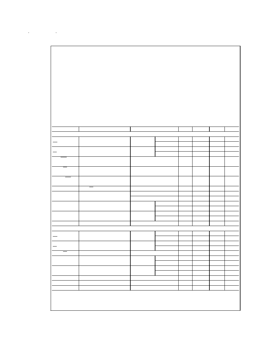
Absolute Maximum Ratings
(Note 2)
If Military/Aerospace specified devices are required,
please contact the National Semiconductor Sales Office/
Distributors for availability and specifications.
Supply Voltage
V
CC
7V
V
EE
-7V
Maximum Power Dissipation (Note 1) at 25°C
Cavity Package
1509 mW
Molded Package
1476 mW
Input Voltage
15V
Output Voltage (Power OFF)
±
15V
Storage Temperature
-65°C to +150°C
Lead Temperature (Soldering, 4 sec.)
260°C
Operating Conditions
Min
Max
Units
Supply Voltage
DS1692
V
CC
4.5
5.5
V
V
EE
-4.5
-5.5
V
DS3692
V
CC
4.75
5.25
V
V
EE
-4.75
-5.25
V
Temperature (T
A
)
DS1692
-55
+125
°C
DS3692
0
+70
°C
Note 1: Derate cavity package 10.1 mW/°C; derate molded package 11.9
mW/°C above 25°C.
Electrical Characteristics
DS1692/DS3692 (Notes 3, 4, 5)
Symbol
Parameter
Conditions
Min
Typ
Max
Units
DS1692, V
CC
= 5V
±
10%, DS3692, V
CC
= 5V
±
5%, V
EE
CONNECTION TO GROUND, MODE SELECT
0.8V
V
O
Differential Output Voltage
R
L
=
V
IN
= 2V
2.5
3.6
V
V
O
V
A,B
V
IN
= 0.8V
-2.5
-3.6
V
V
T
Differential Output Voltage
R
L
= 100
V
IN
= 2V
2
2.6
V
V
T
V
A,B
V
CC
4.75V
V
IN
= 0.8V
-2
-2.6
V
V
OS
, V
OS
Common-Mode Offset
R
L
= 100
2.5
3
V
Voltage
|V
T
| - |V
T
|
Difference in Differential
R
L
= 100
0.05
0.4
V
Output Voltage
|V
OS
| - |V
OS
|
Difference in Common-
R
L
= 100
0.05
0.4
V
Mode Offset Voltage
V
SS
|V
T
- V
T
|
R
L
= 100
, V
CC
4.75V
4.0
4.8
V
I
OX
TRI-STATE Output Current
V
O
-10V
-0.002
-0.15
mA
V
O
15V
0.002
0.15
mA
I
SA
Output Short Circuit Current
V
IN
= 0.4V
V
OA
= 6V
80
150
mA
V
OB
= 0V
-80
-150
mA
I
SB
Output Short Circuit Current
V
IN
= 2.4V
V
OA
= 0V
-80
-150
mA
V
OB
= 6V
80
150
mA
I
CC
Supply Current
18
30
mA
DS1692, V
CC
= 5V
±
10%, V
EE
= -5V
±
10%, DS3692, V
CC
= 5V
±
5%, V
EE
= -5
±
5%, MODE SELECT
0.8V
V
O
Differential Output Voltage
R
L
=
V
IN
= 2.4V
7
8.5
V
V
O
V
A,B
V
IN
= 0.4V
-7
-8.5
V
V
T
Differential Output Voltage
R
L
= 200
V
IN
= 2.4V
6
7.3
V
V
T
V
A,B
V
IN
= 0.4V
-6
-7.3
V
|V
T
| - |V
T
|
Output Unbalance
|V
CC
| = |V
EE
|, R
L
= 200
0.02
0.4
V
I
OX
TRI-STATE Output Current
V
O
= 10V
0.002
0.15
mA
V
O
= -10V
-0.002
-0.15
mA
I
S
+
Output Short Circuit Current
V
O
= 0V
V
IN
= 2.4V
-80
-150
mA
I
S
-
V
IN
= 0.4V
80
150
mA
I
SLEW
Slew Control Current
±
140
µA
I
CC
Positive Supply Current
V
IN
= 0.4V, R
L
=
18
30
mA
I
EE
Negative Supply Current
V
IN
= 0.4V, R
L
=
-10
-22
mA
www.national.com
2
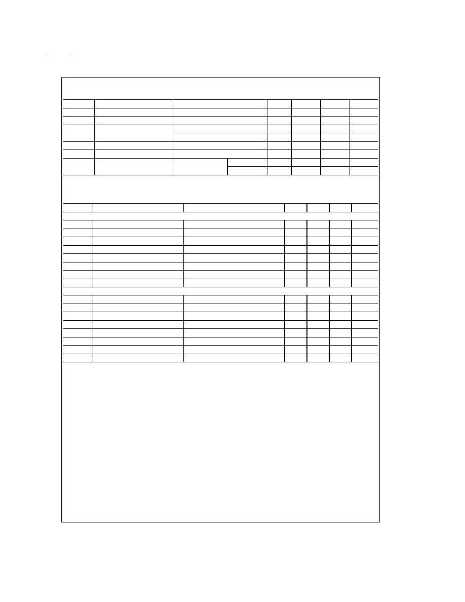
Electrical Characteristics
V
EE
0V (Notes 3, 4)
Symbol
Parameter
Conditions
Min
Typ
Max
Units
V
IH
High Level Input Voltage
2
V
V
IL
Low Level Input Voltage
0.8
V
I
IH
High Level Input Current
V
IN
= 2.4V
1
40
µA
V
IN
15V
10
100
µA
I
IL
Low Level Input Current
V
IN
= 0.4V
-30
-200
µA
V
I
Input Clamp Voltage
I
IN
= -12 mA
-1.5
V
I
XA
Output Leakage Current
V
CC
= V
EE
= 0V
V
O
= 15V
0.01
0.15
mA
I
XB
Power OFF
V
O
= -15V
-0.01
-0.15
mA
Switching Characteristics
T
A
= 25°C
Symbol
Parameter
Conditions
Min
Typ
Max
Units
V
CC
= 5V, MODE SELECT = 0.8V
t
r
Differential Output Rise Time
R
L
= 100
, C
L
= 500 pF (Figure 1)
120
200
ns
t
f
Differential Output Fall Time
R
L
= 100
, C
L
= 500 pF (Figure 1)
120
200
ns
t
PDH
Output Propagation Delay
R
L
= 100
, C
L
= 500 pF (Figure 1)
120
200
ns
t
PDL
Output Propagation Delay
R
L
= 100
, C
L
= 500 pF (Figure 1)
120
200
ns
t
PZL
TRI-STATE Delay
R
L
= 100
, C
L
= 500 pF (Figure 2)
180
250
ns
t
PZH
TRI-STATE Delay
R
L
= 100
, C
L
= 500 pF (Figure 2)
180
250
ns
t
PLZ
TRI-STATE Delay
R
L
= 100
, C
L
= 500 pF (Figure 2)
80
150
ns
t
PHZ
TRI-STATE Delay
R
L
= 100
, C
L
= 500 pF (Figure 2)
80
150
ns
V
CC
= 5V, V
EE
= -5V, MODE SELECT = 0.8V
t
r
Differential Output Rise Time
R
L
= 200
, C
L
= 500 pF (Figure 1)
190
300
ns
t
f
Differential Output Fall Time
R
L
= 200
, C
L
= 500 pF (Figure 1)
190
300
ns
t
PDL
Output Propagation Delay
R
L
= 200
, C
L
= 500 pF (Figure 1)
190
300
ns
t
PDH
Output Propagation Delay
R
L
= 200
, C
L
= 500 pF (Figure 1)
190
300
ns
t
PZL
TRI-STATE Delay
R
L
= 200
, C
L
= 500 pF (Figure 2)
180
250
ns
t
PZH
TRI-STATE Delay
R
L
= 200
, C
L
= 500 pF (Figure 2)
180
250
ns
t
PLZ
TRI-STATE Delay
R
L
= 200
, C
L
= 500 pF (Figure 2)
80
150
ns
t
PHZ
TRI-STATE Delay
R
L
= 200
, C
L
= 500 pF (Figure 2)
80
150
ns
Note 2: "Absolute Maximum Ratings" are those values beyond which the safety of the device cannot be guaranteed. They are not meant to imply that the devices
should be operated at these limits. The table of "Electrical Characteristics" provide conditions for actual device operation.
Note 3: Unless otherwise specified, min/max limits apply across the -55°C to +125°C temperature range for the DS1692 and across the 0°C to +70°C range for the
DS3692. All typicals are given for V
CC
= 5V and T
A
= 25°C. V
CC
and V
EE
as listed in operating conditions.
Note 4: All currents into device pins are positive; all currents out of device pins are negative. All voltages are referenced to ground unless otherwise specified.
Note 5: Only one output at a time should be shorted.
www.national.com
3
AC Test Circuits and Switching Time Waveforms
Switching Waveforms
DS005784-3
DS005784-4
FIGURE 1. Differential Connection
DS005784-5
DS005784-6
FIGURE 2. TRI-STATE Delays for DS1692/DS3692
DS005784-7
DS005784-8
www.national.com
4
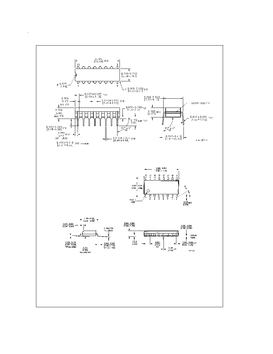
Physical Dimensions
inches (millimeters) unless otherwise noted
Ceramic Dual-In-Line Package (J)
Order Number DS1692J, DS3692J
NS Package Number J16A
Small Outline Package (M)
Order Number DS3692M
NS Package Number M16A
www.national.com
5