
DS36C200
Dual High Speed Bi-Directional Differential Transceiver
General Description
The DS36C200 is a dual transceiver device optimized for
high data rate and low power applications. This device pro-
vides a single chip solution for a dual high speed
bi-directional interface. Also, both control pins may be routed
together for single bit control of datastreams. Both control
pins are adjacent to each other for ease of routing them
together. The DS36C200 is compatible with IEEE 1394
physical layer and may be used as an economical solution
with some considerations. Please reference the application
information on 1394 for more information. The device is in a
14-lead small outline package. The differential driver outputs
provides low EMI with its low output swings typically 210 mV.
The receiver offers
�
100 mV threshold sensitivity, in addition
to common-mode noise protection.
Features
n
Optimized for DSS to DVHS interface link
n
Compatible IEEE 1394 signaling voltage levels
n
Operates above 100 Mbps
n
Bi-directional transceivers
n
14-lead SOIC package
n
Ultra low power dissipation
n
�
100 mV receiver sensitivity
n
Low differential output swing typical 210 mV
n
High impedance during power off
Connection Diagram
01262101
Order Number DS36C200M
See NS Package Number M14A
Note:
*
denotes active LOW pin
Functional Diagram
01262102
May 2001
DS36C200
Dual
High
Speed
Bi-Directional
Differential
T
ransceiver
� 2001 National Semiconductor Corporation
DS012621
www.national.com

Absolute Maximum Ratings
(Note 1)
If Military/Aerospace specified devices are required,
please contact the National Semiconductor Sales Office/
Distributors for availability and specifications.
Supply Voltage (V
CC
)
-0.3V to +6V
Enable Input Voltage
(DE, RE
*
)
-0.3V to (V
CC
+ 0.3V)
Voltage (DI/RO)
-0.3V to +5.9V
Voltage (DO/RI
�
)
-0.3V to +5.9V
Maximum Package Power Dissipation
@
+25�C
M Package
1255 mW
Derate M Package
10.04 mW/�C above +25�C
Storage Temperature Range
-65�C to +150�C
Lead Temperature Range
(Soldering, 4 sec.)
+260�C
ESD Rating (Note 4)
(HBM, 1.5 k
, 100 pF)
3.5 kV
(EIAJ, 0
, 200 pF)
300V
Recommended Operating
Conditions
Min
Typ
Max
Units
Supply Voltage (V
CC
)
+4.5
+5.0
+5.5
V
Receiver Input Voltage
0
2.4
V
Operating Free Air
Temperature (T
A
)
0
25
70
�C
Electrical Characteristics
(Notes 2, 3, 7)
Over supply voltage and operating temperature ranges, unless otherwise specified
Symbol
Parameter
Conditions
Pin
Min
Typ
Max
Units
DIFFERENTIAL DRIVER CHARACTERISTICS (RE
*
= V
CC
)
V
OD
Output Differential Voltage
R
L
= 55
, (
Figure 1)
DO+,
DO-
172
210
285
mV
V
OD
V
OD
Magnitude Change
0
4
35
mV
V
OH
Output High Voltage
1.36
V
V
OL
Output Low Voltage
1.15
V
V
OS
Offset Voltage
1.0
1.25
1.6
V
V
OS
Offset Magnitude Change
0
5
25
mV
I
OZD
TRI-STATE Leakage
V
OUT
= V
CC
or GND
-10
�
1
+10
�A
I
OXD
Power-Off Leakage
V
OUT
= 5.5V or GND, V
CC
= 0V
-10
�
1
+10
�A
I
OSD
Output Short Circuit Current
V
OUT
= 0V
-4
-9
mA
DIFFERENTIAL RECEIVER CHARACTERISTICS (DE = GND)
V
TH
Input Threshold High
V
CM
= 0V to 2.3V
RI+,
RI-
+100
mV
V
TL
Input Threshold Low
-100
mV
I
IN
Input Current
V
IN
= +2.4V or 0V
-10
�
1
+10
�A
V
OH
Output High Voltage
I
OH
= -400 �A
RO
3.8
4.9
V
Inputs Open
3.8
4.9
V
Inputs Terminated, R
t
= 55
3.8
4.9
V
Inputs Shorted, V
ID
= 0V
4.9
V
V
OL
Output Low Voltage
I
OL
= 2.0 mA, V
ID
= -200 mV
0.1
0.4
V
I
OSR
Output Short Circuit Current
V
OUT
= 0V
-15
-60
-100
mA
DEVICE CHARACTERISTICS
V
IH
Input High Voltage
DI,
DE
RE
*
2.0
V
CC
V
V
IL
Input Low Voltage
GND
0.8
V
I
IH
Input High Current
V
IN
= V
CC
or 2.4V
�
1
�
10
�A
I
IL
Input Low Current
V
IN
= GND or 0.4V
�
1
�
10
�A
V
CL
Input Clamp Voltage
I
CL
= -18 mA
-1.5
-0.8
V
I
CCD
Power Supply Current
No Load, DE = RE
*
= V
CC
V
CC
3
7
mA
R
L
= 55
, DE = RE
*
= V
CC
11
17
mA
I
CCR
DE = RE
*
= 0V
6
10
mA
Note 1: "Absolute Maximum Ratings" are those values beyond which the safety of the device cannot be guaranteed. They are not meant to imply that the devices
should be operated at these limits. The table of "Electrical Characteristics" specifies conditions of device operation.
Note 2: Current into device pins is defined as positive. Current out of device pins is defined as negative. All voltages are referenced to ground except V
OD
and V
ID
.
Note 3: All typicals are given for V
CC
= +5.0V and T
A
= +25�C.
Note 4: ESD Rating: HBM (1.5 k
, 100 pF)
3.5 kV
DS36C200
www.national.com
2

Electrical Characteristics
(Notes 2, 3, 7) (Continued)
EIAJ (0
, 200 pF)
300V
Note 5: C
L
includes probe and fixture capacitance.
Note 6: Generator waveform for all tests unless otherwise specified: f = 1 MHz, Z
O
= 50
, t
r
1 ns, t
f
1 ns (0%�100%).
Note 7: The DS36C200 is a current mode device and only function with datasheet specification when a resistive load is applied to the drivers outputs.
Switching Characteristics
Over supply voltage and operating temperature ranges, unless otherwise specified. (Notes 5, 6)
Symbol
Parameter
Conditions
Min
Typ
Max
Units
DIFFERENTIAL DRIVER CHARACTERISTICS
t
PHLD
Differential Propagation Delay High to Low
R
L
= 55
, C
L
= 10 pF
(
Figure 2 and Figure 3)
1.0
2.5
5.5
ns
t
PLHD
Differential Propagation Delay Low to High
1.0
2.6
5.5
ns
t
SKD
Differential Skew |t
PHLD
� t
PLHD
|
0
0.1
2
ns
t
TLH
Transition Time Low to High
0
0.5
2
ns
t
THL
Transition Time High to Low
0
0.5
2
ns
t
PHZ
Disable Time High to Z
R
L
= 55
(
Figure 4 and Figure 5)
0.3
5
20
ns
t
PLZ
Disable Time Low to Z
0.3
5
20
ns
t
PZH
Enable Time Z to High
0.3
10
30
ns
t
PZL
Enable Time Z to Low
0.3
10
30
ns
DIFFERENTIAL RECEIVER CHARACTERISTICS
t
PHLD
Differential Propagation Delay High to Low
C
L
= 10 pF, V
ID
= 200 mV
(
Figure 6 and Figure 7)
1.5
5
9
ns
t
PLHD
Differential Propagation Delay Low to High
1.5
4.6
9
ns
t
SKD
Differential Skew |t
PHLD
� t
PLHD
|
0
0.4
3
ns
t
r
Rise Time
0
1.5
5
ns
t
f
Fall Time
0
1.5
5
ns
t
PHZ
Disable Time High to Z
C
L
= 10 pF
(
Figure 8 and Figure 9)
1
5
20
ns
t
PLZ
Disable Time Low to Z
1
5
20
ns
t
PZH
Enable Time Z to High
0.3
10
30
ns
t
PZL
Enable Time Z to Low
0.3
10
30
ns
Parameter Measurement Information
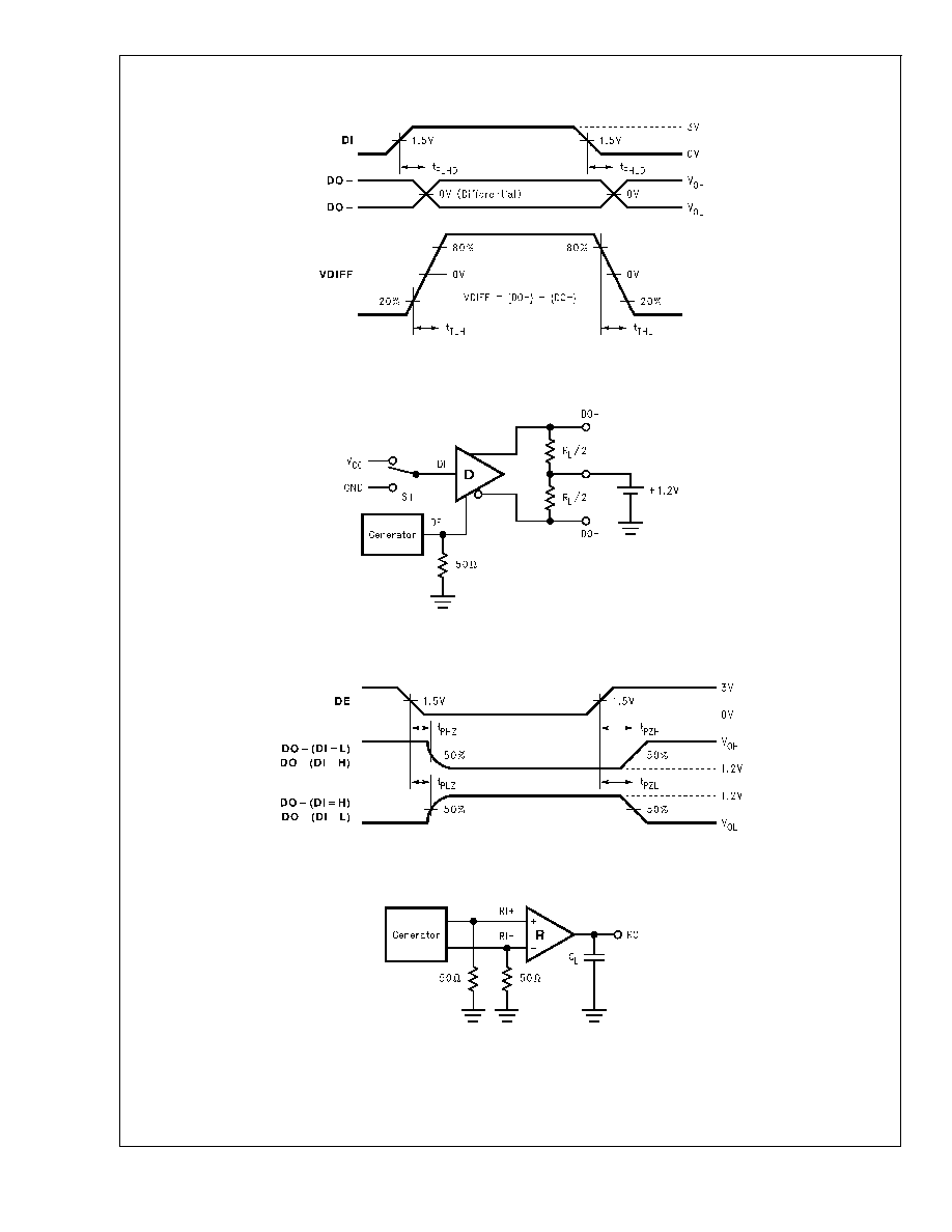
01262103
FIGURE 1. Differential Driver DC Test Circuit
01262104
FIGURE 2. Differential Driver Propagation Delay and Transition Time Test Circuit
DS36C200
www.national.com
3
Parameter Measurement Information
(Continued)
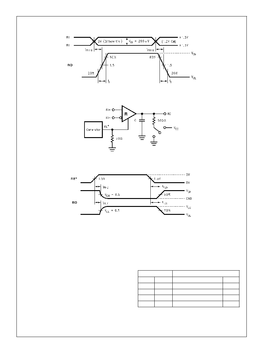
01262105
FIGURE 3. Differential Driver Propagation Delay and Transition Time Waveforms
01262106
FIGURE 4. Driver TRI-STATE Delay Test Circuit
01262107
FIGURE 5. Driver TRI-STATE Delay Waveforms
01262108
FIGURE 6. Receiver Propagation Delay and Transition Time Test Circuit
DS36C200
www.national.com
4
Parameter Measurement Information
(Continued)
Application Information
TRUTH TABLES
The DS36C200 has two enable pins DE and RE
*
, however,
the driver and receiver should never be enabled simulta-
neously. Enabling both could cause multiple channel conten-
tion between the receiver output and the driving logic. It is
recommended to route the enables together on the PC
board. This will allow a single bit [DE/RE
*
] to control the
chip. This DE/RE
*
bit toggles the DS36C200 between Re-
ceive mode and Transmit mode. When the bit is asserted
HIGH the device is in Transmit mode. When the bit is as-
serted LOW the device is in Receive mode. The mode
determines the function of the I/O pins: DI/RO, DO/RI+, and
DO/RI-.Please note that some of the pins have been iden-
tified by its function in the corresponding mode in the three
tables below. For example, in Transmit mode the DO/RI+ pin
is identified as DO+. This was done for clarity in the tables
only and should not be confused with the pin identification
throughout the rest of this document. Also note that a logic
low on the DE/RE
*
bit corresponds to a logic low on both the
DE pin and the RE
*
pin. Similarly, a logic high on the
DE/RE
*
bit corresponds to a logic high on both the DE pin
and the RE
*
pin.
Receive Mode
Input(s)
Input/Output
DE
RE
*
[RI+] - [RI-]
RO
L
L
>
+100 mV
H
L
L
<
-100 mV
L
L
L
100 mV
>
&
>
-100 mV
X
L
H
X
Z
01262109
FIGURE 7. Receiver Propagation Delay and Transition Time Waveforms
01262110
FIGURE 8. Receiver TRI-STATE Delay Test Circuit
01262111
FIGURE 9. Receiver TRI-STATE Delay Waveforms
DS36C200
www.national.com
5