
DS3896/DS3897
BTL Trapezoidal
TM
Transceivers
General Description
These advanced transceivers are specifically designed to
overcome problems associated with driving a densely popu-
lated backplane, and thus provide significant improvement in
both speed and data integrity. Their low output capacitance,
low output signal swing and noise immunity features make
them ideal for driving low impedance buses with minimum
power consumption.
The DS3896 is an octal high speed schottky bus transceiver
with common control signals, whereas the DS3897 is a quad
device with independent driver input and receiver output
pins. The DS3897 has a separate driver disable for each
driver and is, therefore, suitable for arbitration lines. The
separate driver disable pins (En) feature internal pull ups
and may be left open if not required. On the other hand, the
DS3896 provides high package density for data/address
lines.
The open collector drivers generate precise trapezoidal
waveforms, which are relatively independent of capacitive
loading conditions on the outputs. This significantly reduces
noise coupling to adjacent lines. In addition, the receivers
use a low pass filter in conjunction with a high speed com-
parator, to further enhance the noise immunity and provide
equal rejection to both negative and positive going noise
pulses on the bus.
To minimize bus loading, these devices also feature a schot-
tky diode in series with the open collector output that isolates
the driver output capacitance in the disabled state. The out-
put low voltage is typically "1V" and the output high level is
intended to be 2V. This is achieved by terminating the bus
with a pull up resistor to 2V at both ends. The device can
drive an equivalent DC load of 18.5
(or greater) in the
above configuration.
These signalling requirements, including a 1 volt signal
swing, low output capacitance and precise receiver thresh-
olds are referred to as Bus Transceiver Logic (BTL).
Features
n
8 bit DS3896 transceiver provides high package density
n
4 bit DS3897 transceiver provides separate driver input
and receiver output pins
n
BTL compatible
n
Less than 5 pF output capacitance for minimal bus
loading
n
1 Volt bus signal swing reduces power consumption
n
Trapezoidal driver waveforms (t
r
, t
f
6 ns typical)
reduce noise coupling to adjacent lines
n
Temperature insensitive receiver thresholds track the
bus logic high level to maximize noise immunity in both
high and low states
n
Guaranteed A.C. specifications on noise immunity and
propagation delay over the specified temperature and
supply voltage range
n
Open collector driver output allows wire-or connection
n
Advanced low power schottky technology
n
Glitch free power up/down protection on driver and
receiver outputs
n
TTL compatible driver and control inputs and receiver
outputs
Logic Diagrams
Trapezoidal
TM
is a trademark of National Semiconductor Corporation.
DS3896N, M
DS008510-1
DS3897N, M
DS008510-2
Order Numbers DS3896M, DS3896N, DS3897M or DS3897N
See NS Package Number M20B or N20A
January 1996
DS3896/DS3897
BTL
T
rapezoidal
T
ransceivers
� 1999 National Semiconductor Corporation
DS008510
www.national.com

Absolute Maximum Ratings
(Note 1)
If Military/Aerospace specified devices are required,
please contact the National Semiconductor Sales Office/
Distributors for availability and specifications.
Supply Voltage
6V
Control Input Voltage
5.5V
Driver Input and Receiver Output
5.5V
Receiver Input and Driver Output
2.5V
Power Dissipation at 70�C N Package
1480 mW
M Package
TBD mW
Storage Temperature Range
-65�C to +150�C
Lead Temperature (Soldering, 4 sec.)
260�C
Recommended Operating
Conditions
Min
Max
Units
Supply Voltage, V
CC
4.75
5.25
V
Bus Termination Voltage
1.90
2.10
V
Operating Free Air Temperature
0
70
�C
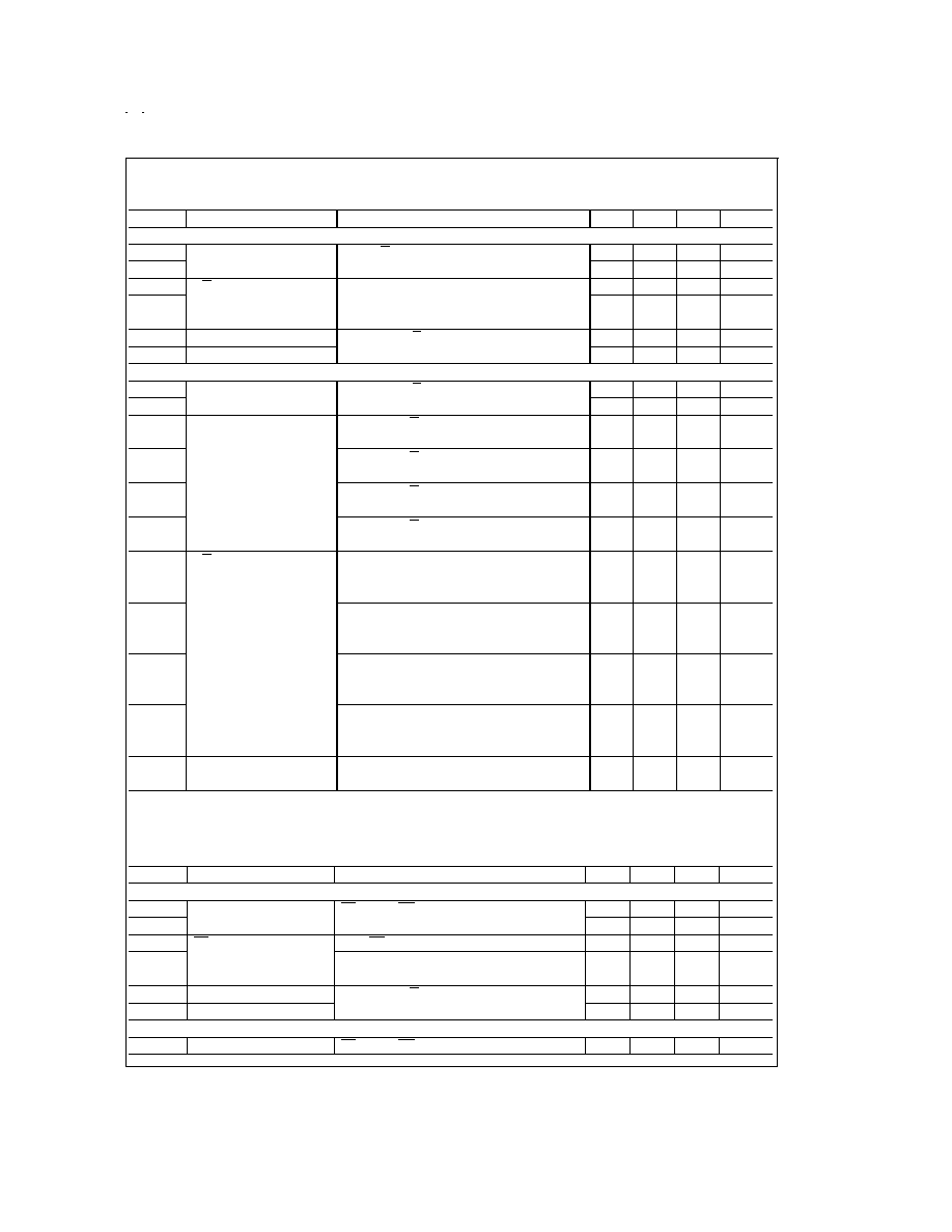
Electrical Characteristics:
(Notes 2, 3)
(0�C
T
A
70�C, 4.75V
V
CC
5.25V unless otherwise specified)
Symbol
Parameter
Conditions
Min
Typ
Max
Units
Driver and Control Inputs: (An, Dn, En, CD, T/R , RE , TE )
V
IH
Logical "1" Input Voltage
2.0
V
V
IL
Logical "0" Input Voltage
0.8
V
I
I
Logical "1" Input Current
An = Dn = En = V
CC
1
mA
I
IH
Logical "1" Input Current
An = Dn = En = 2.4V
40
�A
I
IHC
Logical "1" Input Current
CD = T/R = RE = TE = 2.4V
80
�A
I
IL
Logical "0" Input Current
An = Dn = En = 0.4V
-1
-1.6
mA
I
ILC
Logical "0" Input Current
CD = T/R = RE = TE = 0.4V
-180
-400
�A
V
CL
Input Diode Clamp Voltage
Iclamp = -12 mA
-0.9
-1.5
V
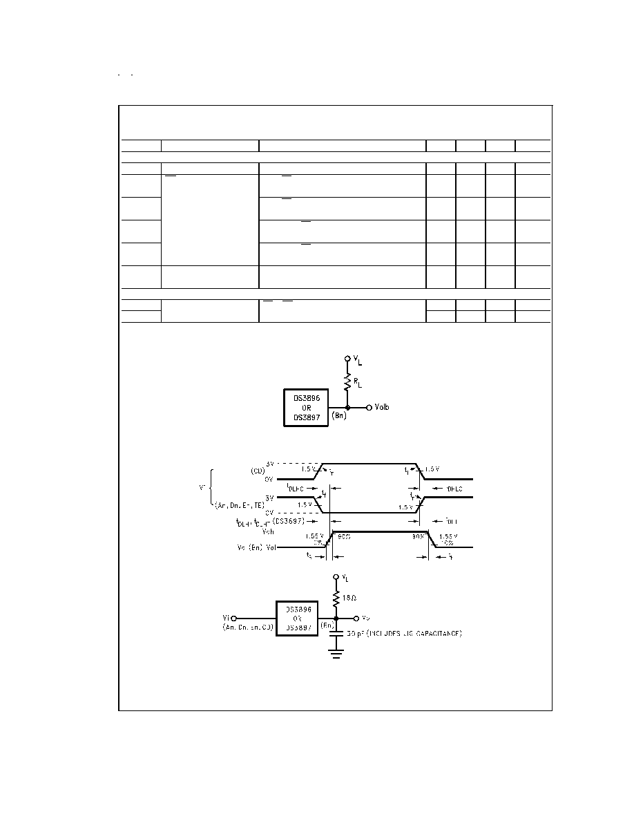
Driver Output/Receiver Input: (Bn)
V
OLB
Low Level Bus Voltage
An = Dn = En = T/R = 2V, VL = 2V
0.75
1.0
1.2
V
RL = 18.5
, CD = TE = 0.8V (
Figure 1)
I
IHB
Maximum Bus Current (Power On)
An = Dn = En = 0.8V, V
CC
= 5.25V
10
100
�A
Bn = 2V
I
ILB
Maximum Bus Current (Power Off)
An = Dn = En = 0.8V, V
CC
= 0V
100
�A
Bn = 2V
V
TH
Receiver Input Threshold
V
CC
= 5V
1.47
1.55
1.62
V
Receiver Output: (An, Rn)
V
OH
Logical "1" Output Voltage
Bn = 1.2V, I
OH
= -400 �A
2.4
3.2
V
CD = T/R = RE = 0.8V
V
OL
Logical "0" Output Voltage
Bn = 2V, I
OL
= 16 mA
0.35
0.5
V
CD = T/R = RE = 0.8V
I
OS
Output Short Circuit Current
Bn = 1.2V
-20
-70
-100
mA
CD = T/R = RE = 0.8V
I
CC
Supply Current (DS3896)
V
CC
= 5.25V
90
135
mA
I
CC
Supply Current (DS3897)
V
CC
= 5.25V
50
80
mA
Note 1: "Absolute maximum ratings" are those beyond which the safety of the device cannot be guaranteed. They are not meant to imply that the device should be
operated at these limits. The table of "Electrical Characteristic" provide conditions for actual device operation.
Note 2: All currents into device pins are positive; all currents out of device pins are negative. All voltages are referenced to device ground unless otherwise specified.
Note 3: All typicals are given for V
CC
= 5V and T
a
= 25�C.
DS3896 Switching Characteristics
(0�C
T
A
70�C, 4.75V
V
CC
5.25V unless otherwise specified)
Symbol
Parameter
Conditions
Min
Typ
Max
Units
Driver:
t
DLH
An to Bn
CD = 0.8V, T/R = 2.0V, VL = 2V
5
9
15
ns
t
DHL
(
Figure 2)
5
9
15
ns
www.national.com
2
DS3896 Switching Characteristics
(Continued)
(0�C
T
A
70�C, 4.75V
V
CC
5.25V unless otherwise specified)
Symbol
Parameter
Conditions
Min
Typ
Max
Units
Driver:
t
DLHC
CD to Bn
An = T/R = 2.0V, VL = 2V
5
10
18
ns
t
DHLC
(
Figure 2)
5
12
20
ns
t
DLHT
T/R to Bn
VCI = An, VC = 5V,
(
Figure 5)
5
15
25
ns
t
DHLT
CD = 0.8V, RC = 390
, CL = 30 pF
5
22
35
ns
RL1 = 18
, RL2 = NC, VL = 2V
t
R
Driver Output Rise Time
CD = 0.8V, T/R = 2V, VL = 2V
3
6
10
ns
t
F
Driver Output Fall Time
(
Figure 2)
3
6
10
ns
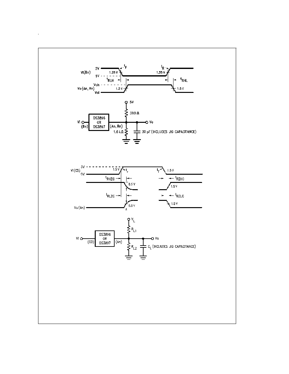
Receiver:
t
RLH
Bn to An
CD = 0.8V, T/R = 0.8V
5
12
18
ns
t
RHL
(
Figure 3)
5
10
18
ns
t
RLZC
CD to An
Bn = 2.0V, T/R = 0.8V, CL = 5 pF
5
10
18
ns
RL1 = 390
, RL2 = NC, VL = 5V
(
Figure 4)
t
RZLC
Bn = 2.0V, T/R = 0.8V, CL = 30 pF
5
8
15
ns
RL1 = 390
, RL2 = 1.6k, VL = 5V
(
Figure 4)
t
RHZC
Bn = 0.8V, T/R = 0.8V, VL = 0V,
2
4
8
ns
RL1 = 390
, RL2 = NC, CL = 5 pF (
Figure 4)
t
RZHC
Bn = 0.8V, T/R = 0.8V, VL = 0V,
3
7
12
ns
RL1 = NC, RL2 = 1.6k, CL = 30 pF
(
Figure 4)
t
RLZT
T/R to An
VCI = Bn, VC = 2V, RC = 18
,
5
10
18
ns
CD = 0.8V, VL = 5V, RL1 = 390
,
RL2 = NC, CL = 5 pF
(
Figure 5)
t
RZLT
VCI = Bn, VC = 2V, RC = 18
,
14
24
40
ns
CD = 0.8V, VL = 5V, RL1 = 390
,
RL2 = 1.6k, CL = 30 pF
(
Figure 5)
t
RHZT
VCI = Bn, VC = 0V, RC = 18
,
2
4
8
ns
CD = 0.8V, VL = 0V, RL1 = 390
,
RL2 = NC, CL = 5 pF
(
Figure 5)
t
RZHT
VCI = Bn, VC = 0V, RC = 18
,
2
8
15
ns
CD = 0.8V, VL = 0V, RL1 = NC
RL2 = 1.6k, CL = 30 pF
(
Figure 5)
t
NR
Receiver Noise
(
Figure 6)
3
6
ns
Rejection Pulse Width
Note: NC means open
DS3897 Switching Characteristics
(0�C
T
A
70�C, 4.75V
V
CC
5.25V unless otherwise specified)
Symbol
Parameter
Conditions
Min
Typ
Max
Units
Driver:
t
DLH
Dn, En to Bn
TE = 0.8V, RE = 2.0V, VL = 2V
5
9
15
ns
t
DHL
(
Figure 2)
5
9
15
ns
t
DLHT
TE to Bn
An = RE = 2.0V, VL = 2V,
(
Figure 2)
5
10
18
ns
t
DHLT
RC = 390
, VCI = An, VC = 5V, CL = 30 pF
5
12
20
ns
RL1 = 18
, RL2 = NC, VL = 2V
(
Figure 5)
t
R
Driver Output Rise Time
CD = 0.8V, T/R = 2V, VL = 2V
3
6
10
ns
tF
Driver Output Fall Time
(
Figure 2)
3
6
10
ns
Receiver:
t
RLH
Bn to Rn
TE = 2.0V, RE = 0.8V
(
Figure 3)
5
10
18
ns
www.national.com
3
DS3897 Switching Characteristics
(Continued)
(0�C
T
A
70�C, 4.75V
V
CC
5.25V unless otherwise specified)
Symbol
Parameter
Conditions
Min
Typ
Max
Units
Receiver:
t
RHL
5
12
18
ns
t
RLZR
RE to Rn
Bn = TE = 2V, VL = 5V, CL = 5 pF
5
10
18
ns
RL1 = 390
, RL2 = NC
(
Figure 4)
t
RZLR
Bn = TE = 2V, VL = 5V, CL = 30 pF
5
8
15
ns
RL1 = 390
, RL2 = 1.6k
(
Figure 4)
t
RHZR
Bn = 0.8V, TE = 2V, VL = 0V,
2
4
8
ns
RL1 = 390
, RL2 = NC, CL = 5 pF
(
Figure 4)
t
RZHR
Bn = 0.8V, TE = 2V, VL = 0V,
3
7
12
ns
RL1 = NC, RL2 = 1.6k, CL = 30 pF
(
Figure 4)
t
NR
Receiver Noise
(
Figure 6)
3
6
ns
Rejection Pulse Width
Driver plus Receiver:
t
DRLH
Dn to Rn
TE = RE = 0.8V
(
Figure 7)
10
20
30
ns
t
DRHL
10
20
30
ns
Note: NC means open
DS008510-3
FIGURE 1. Driver Output Low Voltage Test
DS008510-4
Note: t
r
= t
f
5 ns from 10% to 90%
FIGURE 2. Driver Propagation Delays
www.national.com
4
DS3897 Switching Characteristics
(Continued)
DS008510-5
Note: t
R
= t
F
10 ns from 10% to 90%
FIGURE 3. Receiver Propagation Delays
DS008510-6
Note: t
r
= t
f
5 ns from 10% to 90%
FIGURE 4. Propagation Delay from CD pin to An
www.national.com
5