 | –≠–ª–µ–∫—Ç—Ä–æ–Ω–Ω—ã–π –∫–æ–º–ø–æ–Ω–µ–Ω—Ç: DS38C86A | –°–∫–∞—á–∞—Ç—å:  PDF PDF  ZIP ZIP |

DS38C86A
CMOS BTL 9-Bit Latching Data Transceiver
General Description
The DS38C86A is a 9-bit BTL Latching Data Transceiver de-
signed specifically for proprietary bus interfaces. The device
is implemented in CMOS technology, and delivers all of the
performance of its Bi-CMOS counterparts while consuming
less then half of the power supply current of the DS3886A.
The DS38C86A conforms to the IEEE 11941.1 (Backplane
Transceiver Logic - BTL) Standard.
The DS38C86A incorporates an edge-triggered latch in the
driver path which can be bypassed during fall-through mode
of operation and a transparent latch in the receiver path. The
DS38C86A driver output configuration is an open drain
which allows Wired-OR connection on the bus. A unique de-
sign reduces the bus loading to 3 pF typical. The driver also
has high sink current capability to comply with the bus load-
ing requirements defined within IEEE 11941.1 BTL specifica-
tion.
Backplane Transceiver Logic (BTL) is a signaling standard
that was invented and first introduced by National Semicon-
ductor, then developed by the IEEE to enhance the perfor-
mance of backplane buses. BTL transceivers feature low
output capacitance drivers to minimize bus loading, a 1V
nominal signal swing for reduced power consumption and
receivers with precision thresholds for maximum noise im-
munity. The BTL standard eliminates settling time delays that
severely limit TTL bus performance, and thus provide signifi-
cantly higher bus transfer rates. The backplane bus is in-
tended to be operated with termination resistors (selected to
match the bus impedance) connected to a 2.1V at both ends.
The low voltage is typically 1V.
The DS38C86A provides an alternative to high power Bipo-
lar and BiCMOS devices with the use of CMOS technology.
The CMOS technology enables the DS38C86A to operate at
50% of the I
CC
required by the Bi-CMOS DS3886A. This can
have a major impact on system power consumption. For ex-
ample, if a backplane is 128 bits wide, 16 devices (9 bits
each) required per card. Also assume the backplane is one
rack with 20 slots. Power dissipation savings for this applica-
tion is calculated by the following equation:
P = I
CC
-savings x Power supply voltage x number of devices
P = 32 mA x 5.5V x 320 = 56 Watts
The power dissipation savings may increase even more
when; the system bus is wider than 128 bits, there are mul-
tiple racks in the system, or if the system includes a hot
backup. This may double the power dissipation savings.
Separate ground pins are provided for each BTL output mini-
mize induced ground noise during simultaneous switching.
The unique driver circuitry provides a maximum slew rate of
0.9V/ns which allows controlled rise and fall times to reduce
noise coupling to adjacent lines.
The transceiver's high impedance control and driver inputs
are fully TTL compatible.
The receiver is a high speed comparator that utilizes a Band-
gap reference for precision threshold control allowing maxi-
mum immunity to the BTL 1V signaling level.
Separate QV
CC
and QGND pins are provided to minimize
the effects of high current switching noise. The receiver out-
put is TRI-STATE
Æ
and fully TTL compatible.
The DS38C86A supports live insertion as defined in IEEE
896.2 through the LI (Live Insertion) pin. To implement live
insertion the LI pin should be connected to the live insertion
power connector. If this function is not supported, the LI pin
must be tied to the V
CC
pin. The DS38C86A also provides
glitch free power up/down protection during power sequenc-
ing.
The DS38C86A has two types of power connections in addi-
tion to the LI pin. They are the Logic V
CC
(V
CC
) and the Quiet
V
CC
(QV
CC
). There are two Logic V
CC
pins on the
DS38C86A that provide the supply voltage for the logic and
control circuitry. Multiple connections are provided to reduce
the effects of package inductance and thereby minimize
switching noise. A voltage delta between V
CC
and QV
CC
should never exceed
±
0.5V because of ESD circuitry.
When CD (Chip Disable) is high, An is in high impedance
state and Bn is high. To transmit data (An to Bn), the T/R sig-
nal is high.
When RBYP is high, the positive edge triggered flip-flop is in
the transparent mode. When RBYP is low, the positive edge
of the ACLK signal clocks the data.
In addition, the ESD circuitry between the V
CC
pins and all
other pins except for BTL I/O's and LI pins requires that any
voltage on these pins should not exceed the voltage on V
CC
+0.5V.
There are three different types of ground pins on the
DS38C86A;
the
logic
ground
(GND),
BTL
grounds
(B0GND≠B8GND) and the Bandgap reference ground
(QGND). All of these ground reference pins are isolated
within the chip to minimize the effects of high current switch-
ing transients. For optimum performance the QGND should
be returned to the connector through a quiet channel that
does not carry transient switching current. The GND and
B0GND≠B8GND should be connected to the nearest back-
plane ground pin with the shortest possible path.
Since many different grounding schemes could be imple-
mented and ESD circuitry exists on the DS38C86A, it is im-
portant to note that any voltage between ground pins,
QGND, GND or B0GND≠B8GND should not exceed
±
0.5V
including power up/down sequencing.
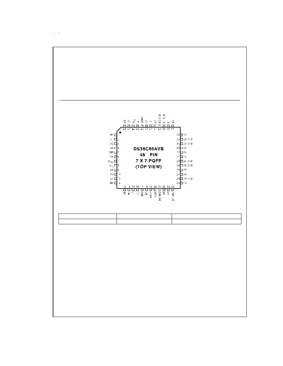
The DS38C86A is offered in a 48-pin 7 x 7 space saving
PQFP package.
TRI-STATE
Æ
is a registered trademark of National Semiconductor Corporation.
July 1998
DS38C86A
CMOS
BTL
9-Bit
Latching
Data
T
ransceiver
© 1999 National Semiconductor Corporation
DS012623
www.national.com
Features
n
>
50% Less I
CC
then Bi-CMOS DS3886A
n
9-Bit inverting BTL latching transceiver
n
Meets IEEE 1194.1 Standard on Backplane Transceiver
Logic (BTL)
n
Very low bus-port capacitance -- 3 pF typical
n
Supports live insertion
n
Glitch free power-up/down protection
n
Fast propagation delays
-- An to Bn (Fall-Thru Mode) 6.0 ns max
-- Bn to An (Bypass Mode) 7.0 ns max
n
1V Signal swings with 80 mA sink capability
n
Open drain bus-port outputs allow Wired-OR connection
n
Controlled rise and fall time to reduce noise coupling to
adjacent lines
n
TTL compatible Driver and Control inputs
n
Built in Bandgap reference with separate QV
CC
and
QGND pins for precise receiver thresholds
n
Individual bus-port ground pins
n
Tight skew --
-- Driver 2.0 ns max
-- Receiver 2.5 ns max
Connection Diagram
Ordering Information
NSID
Package
NS Package Number
DS38C86AVB
PQFP (7x7)
VBH48A
DS012623-3
www.national.com
2
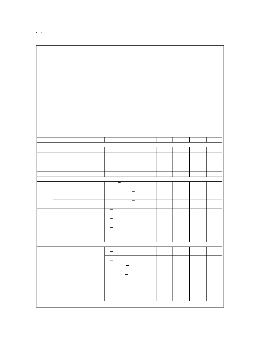
Absolute Maximum Ratings
(Notes 1, 2)
If Military/Aerospace specified devices are required,
please contact the National Semiconductor Sales Office/
Distributors for availability and specifications.
Supply Voltage
(V
CC
, Q
VCC
, LI)
+6.5V
Control Input Voltage
-0.5V to V
CC
+ 0.5V
Driver Input and Receiver
Output (An)
-0.5V to V
CC
+ 0.5V
Receiver Input Current
±
15 mA
Bus Voltage (Bn)
+6.5V
Bus Termination Voltage
+2.4V
ESD Bn Pins (HBM)
2 kV
ESD other Pins (HBM)
(Note 12)
1.5 kV
Power Dissipation at 25∞C
PQFP (7x7) (VF48B)
1.56W
Derate PQFP Package
12.5 mW/∞C
Storage Temperature Range
-65∞C to +150∞C
Lead Temperature
(Soldering, 4 sec.)
260∞C
Recommended Operating
Conditions
Min
Typ
Max
Units
Supply Voltage (V
CC
)
+4.5
+5.0
+5.5
V
Bus Termination Voltage
+2.06
+2.1
+2.14
V
Operating Free Air
Temperature
0
+25
+70
∞C
DC Electrical Characteristics
(Notes 2, 3)
T
A
= 0∞C to +70∞C unless otherwise noted, V
CC
= 5V
±
10%
Symbol
Parameter
Conditions
Min
Typ
Max
Units
DRIVER AND CONTROL INPUTS (CD, T/R, An, ACLK, LE and RBYP)
V
IH
Minimum Input High Voltage
2.0
V
V
IL
Maximum Input Low Voltage
0.8
V
I
IH
Input High Current
V
IN
= V
CC
40
µA
I
IL
Input Low Current
V
IN
= 0V, (except An)
-10
µA
I
IL
Input Low Current
V
IN
= 0V, (An)
-100
µA
V
CL
Input Diode Clamp Voltage
I
CLAMP
= -12 mA
-1.2
V
DRIVER OUTPUT/RECEIVER INPUT (Bn)
V
OLB
Output Low Bus Voltage
(Note 5)
An = T/R = V
CC
, CD = 0V,
I
OL
= 80 mA
0.75
0.9
1.1
V
I
OFF
Output Low Bus Current
An = CD = 0V, T/R = V
CC
,
Bn = 0.75V
-200
µA
Output High Bus Current
An = CD = 0V, T/R = V
CC
,
Bn = 2.1V
300
µA
I
OLBZ
Output Low Bus Current
T/R = CD = V
CC
, Bn = 0.75V
(Chip Disabled)
-100
µA
I
OHBZ
Output High Bus Current
T/R = CD = V
CC
, Bn = 2.1V
(Chip Disabled)
100
µA
V
TH
Receiver Input Threshold
T/R = CD = 0V
1.47
1.55
1.62
V
V
CLP
Positive Clamp Voltage
V
CC
= Max or 0V, I
Bn
= 1 mA
2.4
3.8
4.5
V
V
CLN
Negative Clamp Voltage
I
CLAMP
= -12 mA
-1.2
V
RECEIVER OUTPUT (An)
V
OH
Voltage Output High
Bn = 1.1V, I
OH
= -2 mA,
T/R = CD = 0V
2.5
4.8
V
Bn = 1.1V, I
OH
= -100 µA,
T/R = CD = 0V
4.0
V
V
OL
Voltage Output Low
Bn = 2.1V, T/R = CD = 0V,
I
OL
= 24 mA
0.2
0.5
V
Bn = 2.1V T/R = CD = 0V,
I
OL
= 8 mA
0.1
0.3
V
I
OZ
TRI-STATE Leakage Current
V
IN
= V
CC
, CD = V
CC
,
T/R = 0V, Bn = 0.75V
10
µA
V
IN
= 0.0V, CD = V
CC
,
T/R = 0V, Bn = 0.75V
-10
µA
www.national.com
3
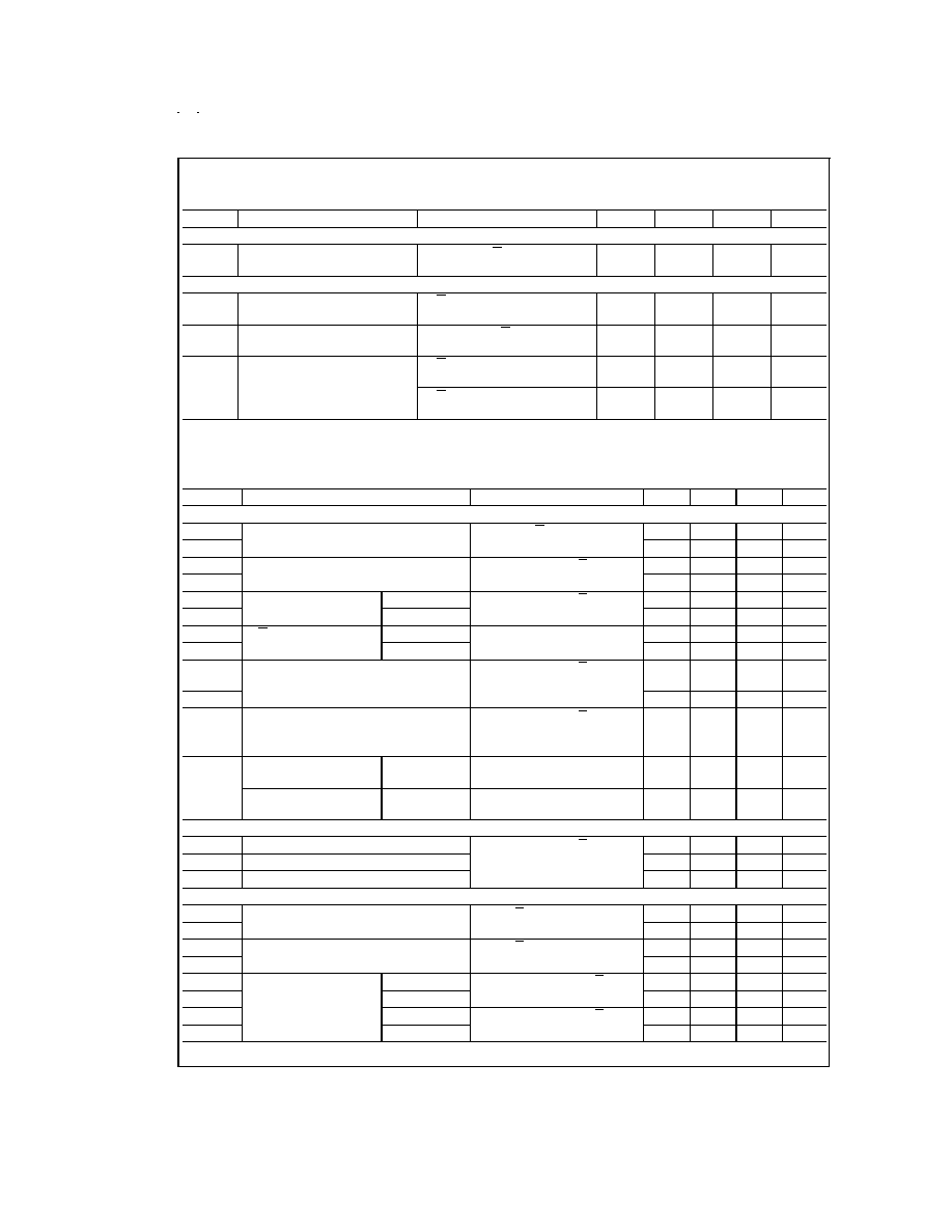
DC Electrical Characteristics
(Notes 2, 3) (Continued)
T
A
= 0∞C to +70∞C unless otherwise noted, V
CC
= 5V
±
10%
Symbol
Parameter
Conditions
Min
Typ
Max
Units
RECEIVER OUTPUT (An)
I
OS
Output Short Circuit Current
Bn = 1.1V, T/R = CD = 0V
(Note 4)
-40
-120
µA
SUPPLY CURRENT
I
CC_DIS
Standby Current (No Load)
T/R = All An = V
CC
, CD = V
CC
,
ACLK = LE = RBYP = V
CC
15
22
mA
I
CCT
Sum of QV
CC
, V
CC
, LI
All Bn = 2.1, T/R = CD = LE =
0.5V, ACLK = RBYP = 3.4
24
31
mA
I
LI
Live Insertion Current
T/R = An = CD = RBYP =
ACLK = 0.0V
1
3
mA
T/R = All An = RBYP = V
CC
,
CD = ACLK = 0V
1
3
mA
AC Electrical Characteristics
(Note 6)
T
A
= 0∞C to +70∞C, V
CC
= 5V
±
10%
DRIVER (REN = 0V for all conditions)
Symbol
Parameter
Conditions
Min
Typ
Max
Units
DRIVER TIMING REQUIREMENTS
t
PHL
An to Bn, Prop Delay
CD = 0V, T/R = RBYP = 3V
2.0
4.3
6.0
ns
t
PLH
Fall-Thru Mode
(
Figures 1, 2)
2.0
3.8
6.0
ns
t
PHL
ACLK to Bn, Prop. Delay
CD = RBYP = 0V, T/R = 3V
2.0
4.5
6.0
ns
t
PLH
Transparent Latch Mode
(
Figures 1, 4)
2.0
4.0
6.0
ns
t
PHL
CD to Bn
Enable Time
CD = RBYP = 0V, T/R = 3V
3
5.3
7.5
ns
t
PLH
Disable Time
(
Figures 1, 3)
2.5
4.3
7.5
ns
t
PHL
T/R to Bn
Enable Time
CD = 0V, RBYP = 3V
9.0
16.0
22.0
ns
t
PLH
Disable Time
(
Figures 10, 11)
2.0
6.6
8.0
ns
t
r
Transition Time-Rise/Fall for Bn
(20% to 80%)
CD = RBYP = 0V, T/R = 3V
0.8
1.4
3.0
ns
t
f
(
Figures 1, 3)(Note 10)
1.0
1.7
3.0
ns
SR
Slew Rate is Calculated from 1.3V to 1.8V
for Bn
CD = RBYP = 0V, T/R = 3V
0.5
0.9
V/ns
(
Figures 1, 2)(Note 10)
t
SKEW
ACLK to Bn, Same
Package
Output to
Output
(Note 7)
0.9
2.5
ns
An to Bn, Same Package
Output to
Output
(Note 7)
0.9
2.0
ns
DRIVER TIMING REQUIREMENTS (
Figure 4)
t
S
An to ACLK (Set-Up Time)
CD = RBYP = 0V, T/R = 3V
3.0
ns
t
H
ACLK to An (Hold Time)
1.0
ns
t
PW
ACLK Pulse Width
3.0
ns
RECEIVER
t
PHL
Bn to An, Prop Delay
CD = T/R = 0V, LE = 3V
3.0
4.8
7.0
ns
t
PLH
Bypass Mode
(
Figures 5, 6)
3.0
5.0
7.0
ns
t
PHL
LE to An, Prop Delay
CD = T/R = 0V
4.0
5.7
7.5
ns
t
PLH
Latch Mode
(
Figures 5, 7)
4.0
5.7
7.5
ns
t
PLZ
CD to An
Disable Time
LE = V
CC
, Bn = 2.1V, T/R = 0V
3.0
6.3
10.0
ns
t
PZL
Enable Time
(
Figures 8, 9)
2.5
3.5
10.0
ns
t
PHZ
Disable Time
LE = V
CC
, Bn = 1.1V, T/R = 0V
4.0
7.3
10.0
ns
t
PZH
Enable Time
(
Figures 8, 9)
3.5
5.5
8.5
ns
www.national.com
4
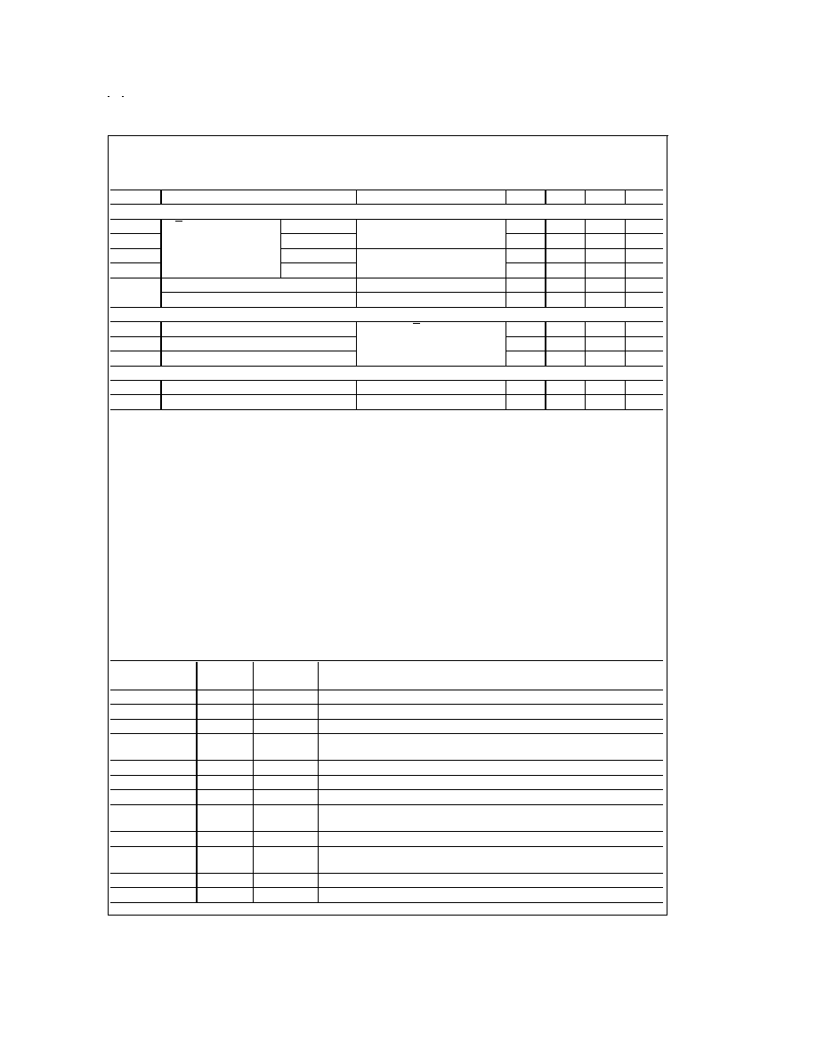
AC Electrical Characteristics
(Note 6) (Continued)
T
A
= 0∞C to +70∞C, V
CC
= 5V
±
10%
DRIVER (REN = 0V for all conditions)
Symbol
Parameter
Conditions
Min
Typ
Max
Units
RECEIVER
t
PLZ
T/R to An
Disable Time
LE = V
CC
, Bn = 2.1V, CD = 0V
3.0
6.0
9.0
ns
t
PZL
Enable Time
(
Figures 10, 11)
3.0
5.0
9.0
ns
t
PHZ
Disable Time
LE = V
CC
, Bn = 1.1 CD = 0V
3.0
7.3
12.0
ns
t
PZH
Enable Time
(
Figures 8, 9)
3.0
5.5
12.0
ns
t
SKEW
LE to An, Same Package
(Note 7)
0.6
2.5
ns
Bn to An, Same Package
(Note 7)
0.7
2.5
ns
RECEIVER TIMING REQUIREMENTS (
Figure 7)
t
S
Bn to LE (Set-Up Time)
CD = 0V, T/R = 0V
3
ns
t
H
LE to Bn (Hold Time)
1
ns
t
PW
LE Pulse Width
5
ns
PARAMETERS NOT TESTED
C
OUTPUT
Capacitance at Bn
(Note 9)
3
pF
t
NR
Noise Rejection
(Note 10)
1
ns
Note 1: "Absolute Maximum Ratings" are these beyond which the safety of the device cannot be guaranteed. They are not meant to imply that the device should
be operated at these limits. The table of "Electrical Characteristics" provides conditions for actual device operation.
Note 2: All input and/or output pins shall not exceed V
CC
+0.5V and shall not exceed the absolute maximum rating at any time, including power-up and power-down.
This prevents the ESD structure from being damaged due to excessive currents flowing from the input and/or output pins to QV
CC
and V
CC
. There is a diode between
each input and/or output to V
CC
which is forward biased when incorrent sequencing is applied. LI and Bn pins do not have power sequencing requirements with re-
spect to V
CC
and QV
CC
. Furthermore, the difference between V
CC
and QV
CC
should never be greater than 0.5V at any time including power-up.
Note 3: All currents into device pins are positive; all currents out of device pins are negative. All voltages are referenced to device ground unless otherwise specified.
All typical values are specified under these conditions: V
CC
= 5V and T
A
= 25∞C, unless otherwise stated.
Note 4: Only one output should be shorted at a time, and duration of the short should not exceed one second.
Note 5: Referenced to appropriate signal ground. Do not exceed maximum power dissipation of package.
Note 6: Input waveforms shall have a rise and fall time of 3 ns.
Note 7: t
SKEW
is the absolute value defined as the difference seen in propagation delay between drivers (receivers) in the same package with identical load con-
ditions.
Note 8: This parameter is tested using TDR techniques described in 1194.0 BTL Backplane Design Guide.
Note 9: This parameter is tested during device characterization. The measurements revealed that the part will reject 1 ns pulse width.
Note 10: Futurebus+ transceivers are required to limit bus signal rise and fall times to no faster then 0.5 V/ns, measured between 1.3V to 1.8V (approximately 20%
to 80% of the nominal voltage swing). The rise and fall times are measured with a transceiver loading equivalent to 12.5
ties to +2.1 V
DC
.
Note 11: Capacitance includes jig and probe capacitance.
Note 12: All pins meet 2 kV typical, one device failure observed between An and QV
CC
in ESD rel sample.
Pin Description
Pin Name
No. of
Pins
Input/Output
Description
A0≠A8
9
I/O
TTL driver input and TRI-STATE receiver output
ACLK
1
I
Clock input for latch mode
B0≠B8
9
I/O
BTL receiver input and driver output
B0 GND≠B8 GND
9
NA
Driver output ground reduces ground bounce due to high current switching of
driver outputs. (Note 11)
CD
1
I
Chip disable
GND
2
NA
Ground reference for switching circuits (Note 11)
LE
1
I
Latch enable
LI
1
NA
Power supply for live insertion. Boards that require live insertion should connect
LI to the live insertion pin on the connector. (Note 12)
NC
9
NA
No connect
QGND
1
NA
Ground reference for receiver input bandgap reference and non-switching
circuits (Note 12)
QV
CC
1
NA
Power supply for bandgap reference and non-switching circuits (Note 12)
RBYP
1
I
Register bypass enable
www.national.com
5