DS42MB200
Dual 4.25 Gb/s 1:2 Mux/Buffer with Input Equalization
and Output Pre-Emphasis
General Description
The DS42MB200 is a dual signal conditioning 2:1 multi-
plexer and 1:2 fan-out buffer designed for use in backplane
redundancy applications. Signal conditioning features in-
clude input equalization and programmable output pre-
emphasis that enable data communication in FR4 back-
planes up to 4 Gb/s. Each input stage has a fixed equalizer
to reduce ISI distortion from board traces. All output drivers
have 4 selectable steps of pre-emphasis to compensate for
transmission losses from long FR4 backplanes and reduce
deterministic jitter. The pre-emphasis levels can be indepen-
dently controlled for the line-side and switch-side drivers.
The internal loopback paths from switch-side input to switch-
side output enable at-speed system testing. All receiver
inputs and driver outputs are internally terminated with 100
differential terminating resistors
Features
n
Dual 2:1 multiplexer and 1:2 buffer
n
1≠ 4.25 Gbps fully differential data paths
n
Fixed input equalization
n
Programmable output pre-emphasis
n
Independent switch and line side pre-emphasis controls
n
Programmable switch-side loopback mode
n
On-chip terminations
n
+3.3V supply
n
Low power, 1W max
n
ESD rating HBM 6 kV
n
Lead-less LLP-48 package (7mmx7mmx0.8mm, 0.5mm
pitch)
n
≠40∞C to +85∞C operating temperature range
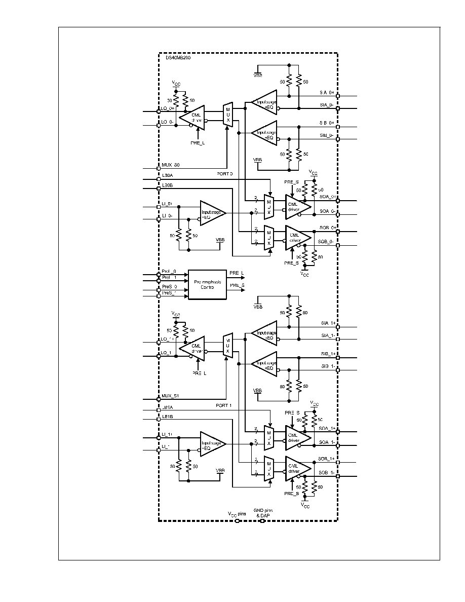
Functional Block Diagram
20178633
July 2006
DS42MB200
Dual
4.25
Gb/s
1:2
Mux/Buffer
with
Input
Equalization
and
Output
Pre-Emphasis
© 2006 National Semiconductor Corporation
DS201786
www.national.com

Pin Descriptions
Pin Name
Pin
Number
I/O
Description
LINE SIDE HIGH SPEED DIFFERENTIAL IO's
LI_0+
LI_0-
6
7
I
Inverting and non-inverting differential inputs of port_0 at the line side. LI_0+ and LI_0-
have an internal 50
connected to an internal reference voltage.
LO_0+
LO_0-
33
34
O
Inverting and non-inverting differential outputs of port_0 at the line side. LO_0+ and LO_0-
have an internal 50
connected to V
CC
.
LI_1+
LI_1-
30
31
I
Inverting and non-inverting differential inputs of port_1 at the line side. LI_1+ and LI_1-
have an internal 50
connected to an internal reference voltage.
LO_1+
LO_1-
9
10
O
Inverting and non-inverting differential outputs of port_1 at the line side. LO_1+ and LO_1-
have an internal 50
connected to V
CC
.
SWITCH SIDE HIGH SPEED DIFFERENTIAL IO's
SOA_0+
SOA_0-
46
45
O
Inverting and non-inverting differential outputs of mux_0 at the switch_A side. SOA_0+ and
SOA_0- have an internal 50
connected to V
CC
.
SOB_0+
SOB_0-
4
3
O
Inverting and non-inverting differential outputs of mux_0 at the switch_B side. SOB_0+ and
SOB_0- have an internal 50
connected to V
CC
.
SIA_0+
SIA_0-
40
39
I
Inverting and non-inverting differential inputs to the mux_0 at the switch_A side. SIA_0+
and SIA_0- have an internal 50
connected to an internal reference voltage.
SIB_0+
SIB_0-
43
42
I
Inverting and non-inverting differential inputs to the mux_0 at the switch_B side. SIB_0+
and SIB_0- have an internal 50
connected to an internal reference voltage.
SOA_1+
SOA_1-
22
21
O
Inverting and non-inverting differential outputs of mux_1 at the switch_A side. SOA_1+ and
SOA_1- have an internal 50
connected to V
CC
.
SOB_1+
SOB_1-
28
27
O
Inverting and non-inverting differential outputs of mux_1 at the switch_B side. SOB_1+ and
SOB_1- have an internal 50
connected to V
CC
.
SIA_1+
SIA_1-
16
15
I
Inverting and non-inverting differential inputs to the mux_1 at the switch_A side. SIA_1+
and SIA_1- have an internal 50
connected to an internal reference voltage.
SIB_1+
SIB_1-
19
18
I
Inverting and non-inverting differential inputs to the mux_1 at the switch_B side. SIB_1+
and SIB_1- have an internal 50
connected to an internal reference voltage.
CONTROL (3.3V LVCMOS)
MUX_S0
37
I
A logic low at MUX_S0 selects mux_0 to switch B. MUX_S0 is internally pulled high.
Default state for mux_0 is switch A.
MUX_S1
13
A logic low at MUX_S1 selects mux_1 to switch B. MUX_S0 is internally pulled high.
Default state for mux_1 is switch A.
PREL_0
PREL_1
12
1
I
PREL_0 and PREL_1 select the output pre-emphasis of the line side drivers (LO_0
±
and
LO_1
±
). PREL_0 and PREL_1 are internally pulled high. See Table 3 for line side
pre-emphasis levels.
PRES_0
PRES_1
36
25
I
PRES_0 and PRES_1 select the output pre-emphasis of the switch side drivers (SOA_0
±
,
SOB_0
±
, SOA_1
±
and SOB_1
±
). PRES_0 and PRES_1 are internally pulled high. See
Table 4 for switch side pre-emphasis levels.
LB0A
47
I
A logic low at LB0A enables the internal loopback path from SIA_0
±
to SOA_0
±
. LB0A is
internally pulled high.
LB0B
48
I
A logic low at LB0B enables the internal loopback path from SIB_0
±
to SOB_0
±
. LB0B is
internally pulled high.
LB1A
23
I
A logic low at LB1A enables the internal loopback path from SIA_1
±
to SOA_1
±
. LB1A is
internally pulled high.
LB1B
24
I
A logic low at LB1B enables the internal loopback path from SIB_1
±
to SOB_1
±
. LB1B is
internally pulled high.
RSV
26
I
Reserve pin to support factory testing. This pin can be left open, or tied to GND, or tied to
GND through an external pull-down resistor.
DS42MB200
www.national.com
4

Pin Descriptions
(Continued)
Pin Name
Pin
Number
I/O
Description
POWER
V
CC
2, 8, 14,
20, 29, 35,
38, 44
P
V
CC
= 3.3V
±
5%.
Each V
CC
pin should be connected to the V
CC
plane through a low inductance path,
typically with a via located as close as possible to the landing pad of the V
CC
pin.
It is recommended to have a 0.01 µF or 0.1 µF, X7R, size-0402 bypass capacitor from
each V
CC
pin to ground plane.
GND
5, 11, 17,
32, 41
P
Ground reference. Each ground pin should be connected to the ground plane through a low
inductance path, typically with a via located as close as possible to the landing pad of the
GND pin.
GND
DAP
P
Die Attach Pad (DAP) is the metal contact at the bottom side, located at the center of the
LLP-48 package. It should be connected to the GND plane with at least 4 via to lower the
ground impedance and improve the thermal performance of the package.
Note: I = Input, O = Output, P = Power
Functional Description
The DS42MB200 is a signal conditioning 2:1 multiplexer and
a 1:2 buffer designed to support port redundancy up to 4.25
Gb/s. Each input stage has a fixed equalizer that provides
equalization to compensate about 5 dB of transmission loss
from a short backplane trace (about 10 inches backplane).
The output driver has pre-emphasis (driver-side equaliza-
tion) to compensate the transmission loss of the backplane
that it is driving. The driver conditions the output signal such
that the lower frequency and higher frequency pulses reach
approximately the same amplitude at the end of the back-
plane, and minimize the deterministic jitter caused by the
amplitude disparity. The DS42MB200 provides 4 steps of
user-selectable pre-emphasis ranging from 0, -3, -6 and ≠9
dB to handle different lengths of backplane. Figure 1 shows
a driver pre-emphasis waveform. The pre-emphasis duration
is 200ps nominal, corresponds to 0.75 bit-width at 4 Gb/s.
The pre-emphasis levels of switch-side and line-side can be
individually programmed.
The high speed inputs are self-biased to about 1.5V and are
designed for AC coupling. The inputs are compatible to most
AC coupling differential signals such as LVDS, LVPECL and
CML.
TABLE 1. LOGIC TABLE FOR MULTIPLEX CONTROLS
MUX_S0
Mux Function
0
MUX_0 select switch_B input, SIB_0
±
.
1 (default)
MUX_0 select switch_A input, SIA_0
±
.
MUX_S1
Mux Function
0
MUX_1 select switch_B input, SIB_1
±
.
1 (default)
MUX_1 select switch_A input, SIA_0
±
.
TABLE 2. LOGIC TABLE FOR LOOPBACK Controls
LB0A
Loopback Function
0
Enable loopback from SIA_0
±
to SOA_0
±
.
1 (default)
Normal mode. Loopback disabled.
LB0B
Loopback Function
0
Enable loopback from SIB_0
±
to SOB_0
±
.
1 (default)
Normal mode. Loopback disabled.
LB1A
Loopback Function
0
Enable loopback from SIA_1
±
to SOA_1
±
.
1 (default)
Normal mode. Loopback disabled.
LB1B
Loopback Function
0
Enable loopback from SIB_1
±
to SOB_1
±
.
1 (default)
Normal mode. Loopback disabled.
DS42MB200
www.national.com
5