
DS75107
Dual Line Receiver
General Description
The product described herein is a TTL compatible dual high
speed circuit intended for sensing in a broad range of system
applications. While the primary usage will be for line receiv-
ers of MOS sensing, the product may effectively be used as
a voltage comparator, level translator, window detector,
transducer preamplifier, and in other sensing applications.
As a digital line receiver the product is applicable with the
SN55109/SN75109 and µA75110/DS75110 companion driv-
ers, or may be used in other balanced or unbalanced
party-line data transmission systems.
Input protection diodes are incorporated in series with the
collectors of the differential input stage. These diodes are
useful in certain applications that have multiple V
CC
+ sup-
plies or V
CC
+ supplies that are turned off.
Features
n
Diode protected input stage for power "OFF" condition
n
17 ns typ high speed
n
TTL compatible
n
±
10 mV or
±
25 mV input sensitivity
n
±
3V input common-mode range
n
High input impedance with normal V
CC
, or V
CC
= 0V
n
Strobes for channel selection
n
Dual circuits
n
Sensitivity gntd. over full common-mode range
n
Logic input clamp diodes -- meets both "A" and "B"
version specifications
n
±
5V standard supply voltages
Connection Diagram
Selection Guide
Temperature
0∞C
T
A
+70∞C
Package
Cavity or Molded Dip
Input Sensitivity
±
25 mV
±
10 mV
Output Logic
TTL Active Pull-Up
DS75107
TTL Open Collector
Dual-In-Line Package
DS009446-1
Top View
Order Number DS75107M, DS75107N
See NS Package Number M14A or N14A
For Complete Military 883 Specifications, see RETS Datasheet.
Order Number DS55107AJ/883
See NS Package Number J14A
May 1999
DS75107
Dual
Line
Receiver
© 1999 National Semiconductor Corporation
DS009446
www.national.com
Absolute Maximum Ratings
(Note 1)
If Military/Aerospace specified devices are required,
please contact the National Semiconductor Sales Office/
Distributors for availability and specifications.
Supply Voltage, V
CC
+
7V
Supply Voltage, V
CC
-
-7V
Differential Input Voltage
±
6V
Common Mode Input Voltage
±
5V
Strobe Input Voltage
5.5V
Storage Temperature Range
-65∞C to +150∞C
Maximum Power Dissipation (Note 1) at 25∞C
Cavity Package
1308 mW
Molded Package
1207 mW
Lead Temperature (Soldering, 4 sec)
260∞C
Note: Derate cavity package 8.7 mW/∞C above 25∞C; derate molded package
9.7 mW/∞C above 25∞C.
Operating Conditions
DS75107
Min
Nom
Max
Supply Voltage V
CC
+
4.75V
5V
5.25V
Supply Voltage V
CC
-
-4.75V
-5V
-5.25V
Operating Temperature Range
0∞C
to
+70∞C
DS75107
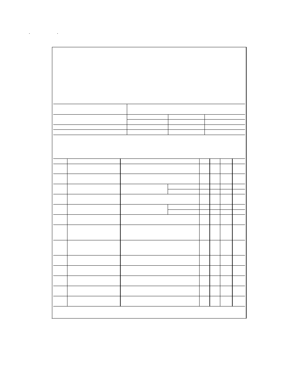
Electrical Characteristics
T
MIN
T
A
T
MAX
(Notes 2, 3)
Symbol
Parameter
Conditions
Min
Typ
Max
Units
I
IH
High Level Input Current
V
CC+
= Max, V
CC-
= Max,
30
75
µA
into A1, B1, A2 or B2
V
ID
= 0.5V, V
IC
= -3V to 3V
I
IL
Low Level Input Current
V
CC+
= Max, V
CC-
= Max,
-10
µA
into A1, B1, A2 or B2
V
ID
= -2V, V
IC
= -3V to 3V
I
IH
High Level Input Current
V
CC+
= Max,
V
IH(S)
= 2.4V
40
µA
into G1 or G2
V
CC-
= Max
V
IH(S)
Max V
CC+
1
mA
I
IL
Low Level Input Current
V
CC+
= Max, V
CC-
= Max,
-1.6
mA
into G1 or G2
V
IL(S)
= 0.4V
I
IH
High Level Input Current into S
V
CC+
= Max,
V
IH(S)
= 2.4V
80
µA
V
CC-
= Max
V
IH(S)
= Max V
CC+
2
mA
I
IL
Low Level Input Current into S
V
CC+
= Max, V
CC-
= Max,
-3.2
mA
V
IL(S)
= 0.4V
V
OH
High Level Output Voltage
V
CC+
= Min, V
CC-
= Min,
I
LOAD
= -400 µA, V
ID
= 25 mV,
2.4
V
V
IC
= -3V to 3V, (Note 3)
V
OL
Low Level Output Voltage
V
CC+
= Min, V
CC-
= Min,
I
SINK
= 16 mA, V
ID
= -25 mV,
0.4
V
V
IC
= -3V to 3V
I
OH
High Level Output Current
V
CC+
= Min, V
CC-
= Min
250
µA
V
OH
= Max V
CC+
I
OS
Short Circuit Output Current
V
CC+
= Max, V
CC-
= Max,
-18
-70
mA
(Notes 3, 5)
I
CCH+
High Logic Level Supply
V
CC+
= Max, V
CC-
= Max,
18
30
mA
Current from V
CC
V
ID
= 25 mV, T
A
= 25∞C
I
CCH-
High Logic Level Supply
V
CC+
= Max, V
CC-
= Max,
-8.4
-15
mA
Current from V
CC
V
ID
= 25 mV, T
A
= 25∞C
V
I
Input Clamp Voltage on G or S
V
CC+
= Min, V
CC-
= Min,
-1
-1.5
V
I
IN
= -12 mA, T
A
= 25∞C
www.national.com
2
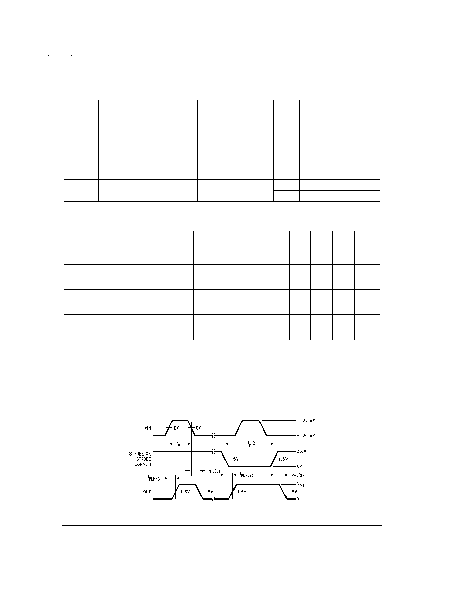
Switching Characteristics
V
CC+
= 5V, V
CC-
= -5V, T
A
= 25∞C
Symbol
Parameter
Conditions
Min
Typ
Max
Units
t
PLH(D)
Propagation Delay Time, Low to
High Level, from Differential Inputs
A and B to Output
R
L
= 390
, C
L
= 50 pF,
(Note 4)
17
25
ns
19
25
ns
t
PHL(D)
Propagation Delay Time, High to
Low Level, from Differential Inputs
A and B to Output
R
L
= 390
, C
L
= 50 pF,
(Note 4)
17
25
ns
19
25
ns
t
PLH(S)
Propagation Delay Time, Low to
High Level, from Strobe Input G or
S to Output
R
L
= 390
, C
L
= 50 pF
10
15
ns
13
20
ns
t
PHL(S)
Propagation Delay Time, High to
Low Level, from Strobe Input G or
S to Output
R
L
= 390
, C
L
= 50 pF
8
15
ns
13
20
ns
Switching Characteristics
V
CC+
= 5V, V
CC-
= -5V, T
A
= 25∞C
Symbol
Parameter
Conditions
Min
Typ
Max
Units
t
PLH(D)
Propagation Delay Time, Low-to-
R
L
= 470
, C
L
= 15 pF, (Note 6)
High Level, from Differential
35
ns
Inputs A and B to Output
t
PHL(D)
Propagation Delay Time, High-to-
R
L
= 470
, C
L
= 15 pF, (Note 6)
Low Level, from Differential
20
ns
Inputs A and B to Output
t
PLH(S)
Propagation Delay Time, Low-to-
R
L
= 470
, C
L
= 15 pF
High Level, from Strobe Input G
17
ns
or S to Output
t
PHL(S)
Propagation Delay Time, High-to-
R
L
= 470
, C
L
= 15 pF
Low Level, from Strobe Input G
17
ns
or S to Output
Note 1: "Absolute Maximum Ratings" are those values beyond which the safety of the device cannot be guaranteed. Except for "Operating Temperature Range" they
are not meant to imply that the devices should be operated at these limits. The table of "Electrical Characteristics" provides conditions for actual device operation.
Note 2: Unless otherwise specified min/max limits apply across the 0∞C to +70∞C range for the DS75107. All typical values are for T
A
= 25∞C and V
CC
= 5V.
Note 3: All currents into device pins shown as positive, out of device pins as negative, all voltages referenced to ground unless otherwise noted. All values shown
as max or min on absolute value basis.
Note 4: Differential input is +100 mV to -100 mV pulse. Delays read from 0 mV on input to 1.5V on output.
Note 5: Only one output at a time should be shorted.
Note 6: Differential input is +10 mV to -30 mV pulse. Delays read from 0 mV on input to 1.5V on output.
Voltage Waveforms
DS009446-12
www.national.com
3
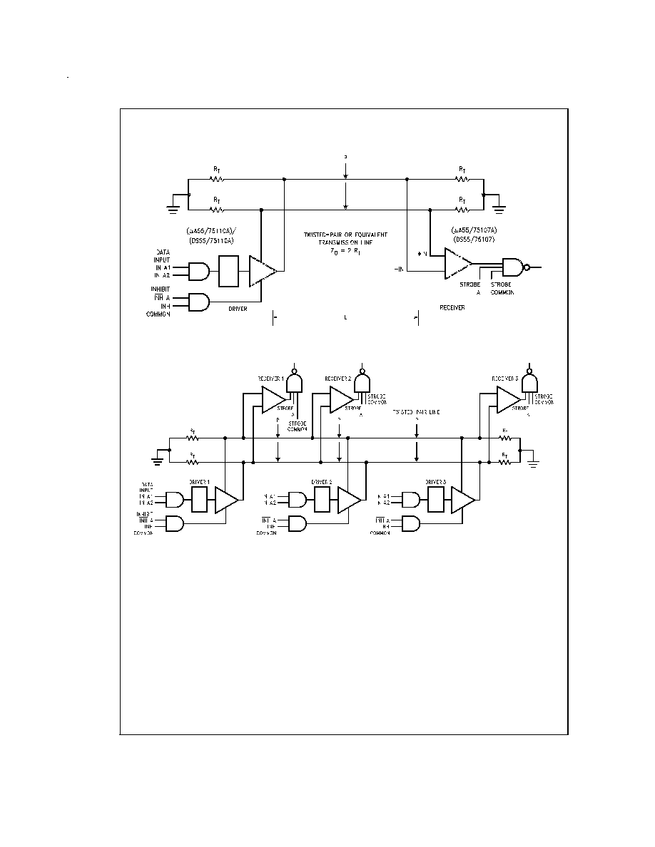
Typical Applications
APPLICATION
The DS75107 dual line circuit is designed specifically for use
in high speed data transmission systems that utilize bal-
anced, terminated transmission lines such as twisted-pair
lines. The system operates in the balanced mode, so that
noise induced on one line is also induced on the other. The
noise appears common mode at the receiver input terminals
where it is rejected. The ground connection between the line
driver and receiver is not part of the signal circuit so that sys-
tem performance is not affected by circulating ground cur-
rents.
The unique driver output circuit allows terminated transmis-
sion lines to be driven at normal line impedances. High
speed system operation is ensured since line reflections are
virtually
eliminated
when
terminated
lines
are
used.
Cross-talk is minimized by low signal amplitudes and low line
impedances.
The typical data delay in a system is approximately (30 +
1.3L) ns, where L is the distance in feet separating the driver
and receiver. This delay includes one gate delay in both the
driver and receiver.
Data is impressed on the balanced-line system by unbalanc-
ing the line voltages with the driver output current. The
driven line is selected by appropriate driver input logic levels.
The voltage difference is approximately:
V
DIFF
1
/
2
I
O(on)
x R
T
:
(1)
High series line resistance will cause degradation of the sig-
nal. The receivers, however, will detect signals as low as
25 mV(or less). For normal line resistances, data may be re-
covered from lines of several thousand feet in length.
Line termination resistors (R
T
) are required only at the ex-
treme ends of the line. For short lines, termination resistors
at the receiver only may prove adequate. The signal ampli-
tude will then be approximately:
V
DIFF
I
O(on)
x R
T
:
(2)
Data-Bus or Party-Line System
DS009446-2
Data-Bus or Party-Line System
DS009446-3
www.national.com
4
Typical Applications
(Continued)
The strobe feature of the receiver and the inhibit feature of
the driver allows the DS75107 dual line circuit to be used in
data-bus or party-line systems. In these applications, several
drivers and receivers may share a common transmission
line. An enabled driver transmits data to all enabled receiv-
ers on the line while other drivers and receivers are disabled.
Data is thus time multiplexed on the transmission line.
DS75107 device specifications allow widely varying thermal
and electrical environments at the various driver and re-
ceiver locations. The data-bus system offers maximum per-
formance at minimum cost.
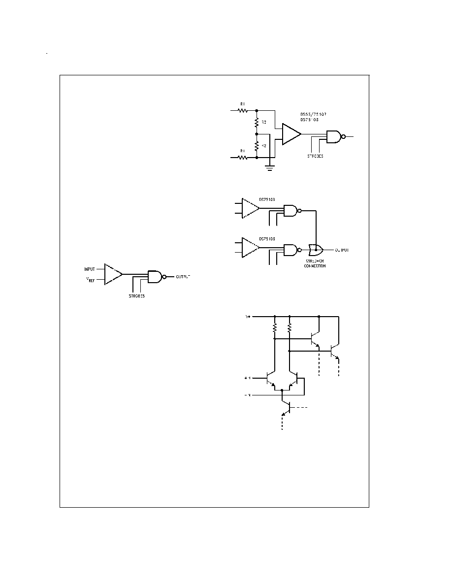
The DS75107 dual line circuits may also be used in unbal-
anced or single line systems. Although these systems do not
offer the same performance as balanced systems for long
lines, they are adequate for very short lines where environ-
ment noise is not severe.
The receiver threshold level is established by applying a DC
reference voltage to one receiver input terminal. The signal
from the transmission line is applied to the remaining input.
The reference voltage should be optimized so that signal
swing is symmetrical about it for maximum noise margin.
The reference voltage should be in the range of -3.0V to
+3.0V. It can be provided by a voltage supply or by a voltage
divider from an available supply voltage.
Precautions in the Use of DS1603, DS3603, DS55107,
DS75107, DS75108 and DS75208 Dual Line Receivers
The following precaution should be observed when using or
testing DS75107 line circuits.
When only one receiver in a package is being used, at least
one of the differential inputs of the unused receiver should
be terminated at some voltage between -3.0V and +3.0V,
preferably at ground. Failure to do so will cause improper op-
eration of the unit being used because of common bias cir-
cuitry for the current sources of the two receivers.
The DS75107 line receiver features a common mode input
voltage range of
±
3.0V. This satisfies the requirements for all
but the noisiest system applications. For these severe noise
environments, the common mode range can be extended by
the use of external input attenuators. Common mode input
voltages can in this way be reduced to
±
3.0V at the receiver
input terminals. Differential data signals will be reduced pro-
portionately. Input sensitivity, input impedance and delay
times will be adversely affected.
Circuit Differences Between "A" and Standard Devices
The difference between the "A" and standard devices is
shown in the following schematics of the input stage.
Unbalanced or Single-Line Systems
DS009446-4
Increasing Common Mode Input
Voltage Range of Receiver
DS009446-5
DS75108 Wired-OR Output Connections
DS009446-6
"A" Devices
DS009446-7
www.national.com
5