 | –≠–ª–µ–∫—Ç—Ä–æ–Ω–Ω—ã–π –∫–æ–º–ø–æ–Ω–µ–Ω—Ç: DS55113 | –°–∫–∞—á–∞—Ç—å:  PDF PDF  ZIP ZIP |

TL F 5785
DS55113DS75113
Dual
TRI-STATE
Differential
Line
Driver
February 1996
DS55113 DS75113 Dual TRI-STATE
Differential Line Driver
General Description
The DS55113 DS75113 dual differential line drivers with
TRI-STATE outputs are designed to provide all the features
of the DS55114 DS75114 line drivers with the added fea-
ture of driver output controls There are individual controls
for each output pair as well as a common control for both
output pairs When an output control is low the associated
output is in a high-impedance state and the output can nei-
ther drive nor load the bus This permits many devices to be
connected together on the same transmission line for party-
line applications
The output stages are similar to TTL totem-pole outputs but
with the sink outputs YS and ZS and the corresponding
active pull-up terminals YP and ZP available on adjacent
package pins
Features
Y
Each circuit offers a choice of open-collector or active
pull-up (totem-pole) outputs
Y
Single 5V supply
Y
Differential line operation
Y
Dual channels
Y
TTL LS compatibility
Y
High-impedance output state for party-line applications
Y
Short-circuit protection
Y
High current outputs
Y
Single-ended or differential AND NAND outputs
Y
Common and individual output controls
Y
Clamp diodes at inputs
Y
Easily adaptable to DS55114 DS75114 applications
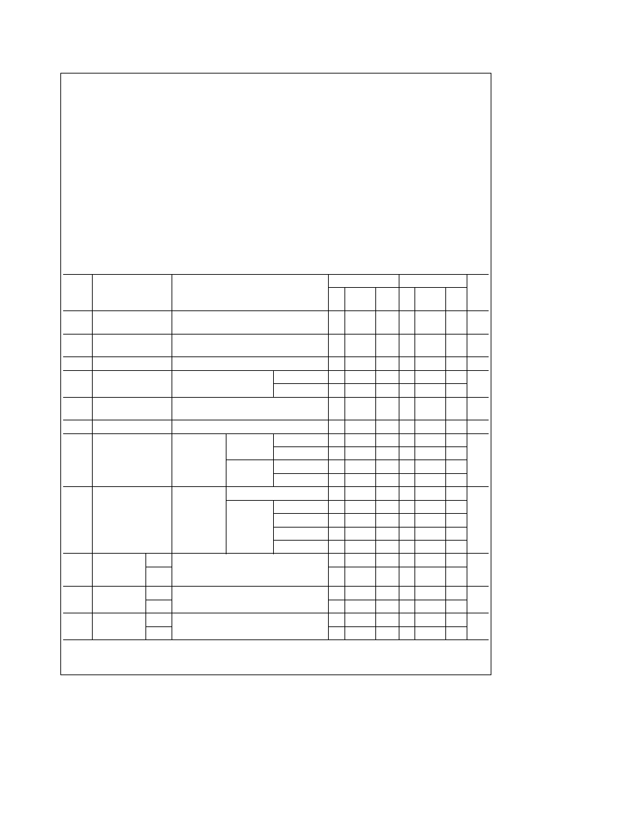
Connection Diagram
Dual-In-Line Package
Positive logic Y
e
AB
Z
e
AB
Output is OFF when
C or CC is low
TL F 5785 ≠ 1
Top View
Order Number DS55113J DS75113M or DS75113N
See NS Package Number J16A M16A or N16A
For Complete Military 883 Specifications see RETS Datasheet
Order Number DS55113J 883
See NS Package Number J16A
Truth Table
Inputs
Outputs
Output Control
Data
AND
NAND
C
CC
A
B
Y
Z
H
e
high level
L
e
low level
L
X
X
X
Z
Z
X
e
irrelevant
Z
e
high impedance (OFF)
X
L
X
X
Z
Z
B input and 4th line of truth
H
H
L
X
L
H
table applicable only to
H
H
X
L
L
H
driver number 1
H
H
H
H
H
L
TRI-STATE
is a registered trademark of National Semiconductor Corp
C1996 National Semiconductor Corporation
RRD-B30M36 Printed in U S A
http
www national com
Absolute Maximum Ratings
(Note 1)
If Military Aerospace specified devices are required
please contact the National Semiconductor Sales
Office Distributors for availability and specifications
Supply Voltage (V
CC
) (Note 1)
7V
Input Voltage
5 5V
OFF-State Voltage Applied to
Open-Collector Outputs
12V
Maximum Power Dissipation at 25 C
Cavity Package
1433 mW
Molded DIP Package
1362 mW
SO Package
1002 mW
Operating Free-Air Temperature Range
DS55113
b
55 C to
a
125 C
DS75113
0 C to
a
70 C
Derate cavity package 9 6 mW C above 25 C derate molded DIP pack-
age 10 9 mW C above 25 C derate SO package 8 01 mW C above 25 C
(Note 2)
Storage Temperature Range
b
65 C to
a
150 C
Lead Temperature (1 16
from case for
60 seconds) J Package
300 C
Lead Temperature (1 16
from case for
4 seconds) N Package
260 C
Operating Conditions
Min
Max
Units
Supply Voltage (V
CC
)
DS55113
4 5
5 5
V
DS75113
4 75
5 25
V
High Level Output Current (I
OH
)
b
40
mA
Low Level Output Current (I
OL
)
40
mA
Operating Free-Air Temperature (T
A
)
DS55113
b
55
125
C
DS75113
0
70
C
Electrical Characteristics
Over recommended operating free-air temperature range (unless otherwise noted)
DS55113
DS75113
Symbol
Parameter
Conditions (Note 3)
Min
Typ
Max Min
Typ
Max
Units
(Note 4)
(Note 4)
V
IH
High Level
2
2
V
Input Voltage
V
IL
Low Level
0 8
0 8
V
Input Voltage
V
IK
Input Clamp Voltage
V
CC
e
Min I
I
e b
12 mA
b
0 9
b
1 5
b
0 9
b
1 5
V
V
OH
High Level
V
CC
e
Min V
IH
e
2V
I
OH
e b
10 mA 2 4
3 4
2 4
3 4
V
Output Voltage
V
IL
e
0 8V
I
OH
e b
40 mA
2
3 0
2
3 0
V
OL
Low Level
V
CC
e
Min V
IH
e
2V V
IL
e
0 8V I
OL
e
40 mA
0 23
0 4
0 23
0 4
V
Output Voltage
V
OK
Output Clamp Voltage
V
CC
e
Max I
O
e b
40 mA
b
1 1
b
1 5
b
1 1
b
1 5
V
I
O(off)
Off-State
V
CC
e
Max
V
OH
e
12V
T
A
e
25 C
1
10
Open-Collector
T
A
e
125 C
200
m
A
Output Current
V
OH
e
5 25V T
A
e
25 C
1
10
T
A
e
70 C
20
I
OZ
Off-State (High-
V
CC
e
Max
T
A
e
25 C V
O
e
0 to V
CC
g
10
g
10
Impedance-State)
Output Controls
T
A
e
Max
V
O
e
0V
b
150
b
20
Output Current
at 0 8V
V
O
e
0 4V
g
80
g
20
m
A
V
O
e
2 4V
g
80
g
20
V
O
e
V
CC
80
20
I
I
Input Current at A B C V
CC
e
Max V
I
e
5 5V
1
1
mA
Maximum Input
CC
2
2
Voltage
I
IH
High Level
A B C V
CC
e
Max V
I
e
2 4V
40
40
m
A
Input Current
CC
80
80
I
IL
Low Level
A B C V
CC
e
Max V
I
e
0 4V
b
1 6
b
1 6
mA
Input Current
CC
b
3 2
b
3 2
http
www national com
2
Electrical Characteristics
Over recommended operating free-air temperature range (unless otherwise noted) (Continued)
DS55113
DS75113
Symbol
Parameter
Conditions (Note 3)
Min
Typ
Max
Min
Typ
Max
Units
(Note 4)
(Note 4)
I
OS
Short-Circuit Output
V
CC
e
Max V
O
e
0V
b
40
b
90
b
120
b
40
b
90
b
120
mA
Current (Note 5)
I
CC
Supply Current
All Inputs at 0V No Load
V
CC
e
Max
47
65
47
65
mA
(Both Drivers)
T
A
e
25 C
V
CC
e
7V
65
85
65
85
Note 1
All voltage values are with respect to network ground terminal
Note 2
For operation above 25 C free-air temperature refer to Dissipation Derating Curves in the Thermal information section
Note 3
All parameters with the exception of OFF-state open-collector output current are measured with the active pull-up connected to the sink output
Note 4
All typical values are at T
A
e
25 C and V
CC
e
5V with the exception of I
CC
at 7V
Note 5
Only one output should be shorted at a time and duration of the short-circuit should not exceed one second
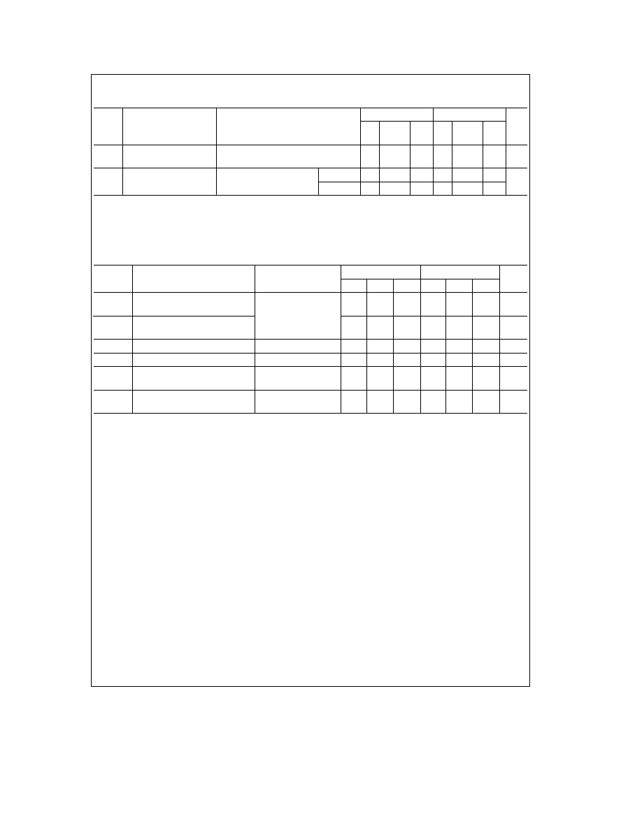
Switching Characteristics
V
CC
e
5V C
L
e
30 pF T
A
e
25 C
Symbol
Parameter
Conditions
DS55113
DS75113
Unit
Min
Typ
Max
Min
Typ
Max
t
PLH
Propagation Delay Time Low-to
(Figure 1)
13
20
13
30
ns
High-Level Output
t
PHL
Propagation Delay Time High-to
12
20
12
30
ns
Low-Level Output
t
PZH
Output Enable Time to High Level
R
L
e
180X
(Figure 2)
7
15
7
20
ns
t
PZL
Output Enable Time to Low Level
R
L
e
250X
(Figure 3)
14
30
14
40
ns
t
PHZ
Output Disable Time from High
R
L
e
180X
(Figure 2)
10
20
10
30
ns
Level
t
PLZ
Output Disable Time from Low
R
L
e
250X
(Figure 3)
17
35
17
35
ns
Level
http
www national com
3

Schematic Diagram
(One side shown only)
These
components
common
to
both
drivers
Resistor
values
shown
are
typical
and
in
X
TLF5785
≠
2
http
www national com
4

AC Test Circuits and Switching Time Waveforms
TL F 5785 ≠ 3
FIGURE 1 t
PLH
and t
PHL
TL F 5785 ≠ 4
FIGURE 2 t
PZH
and t
PHZ
TL F 5785 ≠ 5
FIGURE 3 t
PZL
and t
PLZ
Note 1
The pulse generator has the following characteristics Z
OUT
e
50X PRR
e
500 kHz t
W
e
100 ns
Note 2
C
L
includes probe and jig capacitance
http
www national com
5