 | –≠–ª–µ–∫—Ç—Ä–æ–Ω–Ω—ã–π –∫–æ–º–ø–æ–Ω–µ–Ω—Ç: DS55493 | –°–∫–∞—á–∞—Ç—å:  PDF PDF  ZIP ZIP |
TL F 7561
DS55493DS75493
Quad
LED
Segment
Driver
April 1990
DS55493 DS75493 Quad LED Segment Driver
General Description
The DS55493 DS75493 is a quad LED segment driver It is
designed to interface between MOS IC's and LED's An ex-
ternal resistor is required for each segment to drive the out-
put current which is approximately equal to 0 7V R
L
and is
relatively constant independent of supply variations Blank-
ing can be achieved by taking the chip enable (CE) to a
logical ``1'' level
Features
Y
Low voltage operation
Y
Low input current for MOS compatibility
Y
Low standby power
Y
Display blanking capability
Y
Output current regulation
Y
Quad high gain circuits
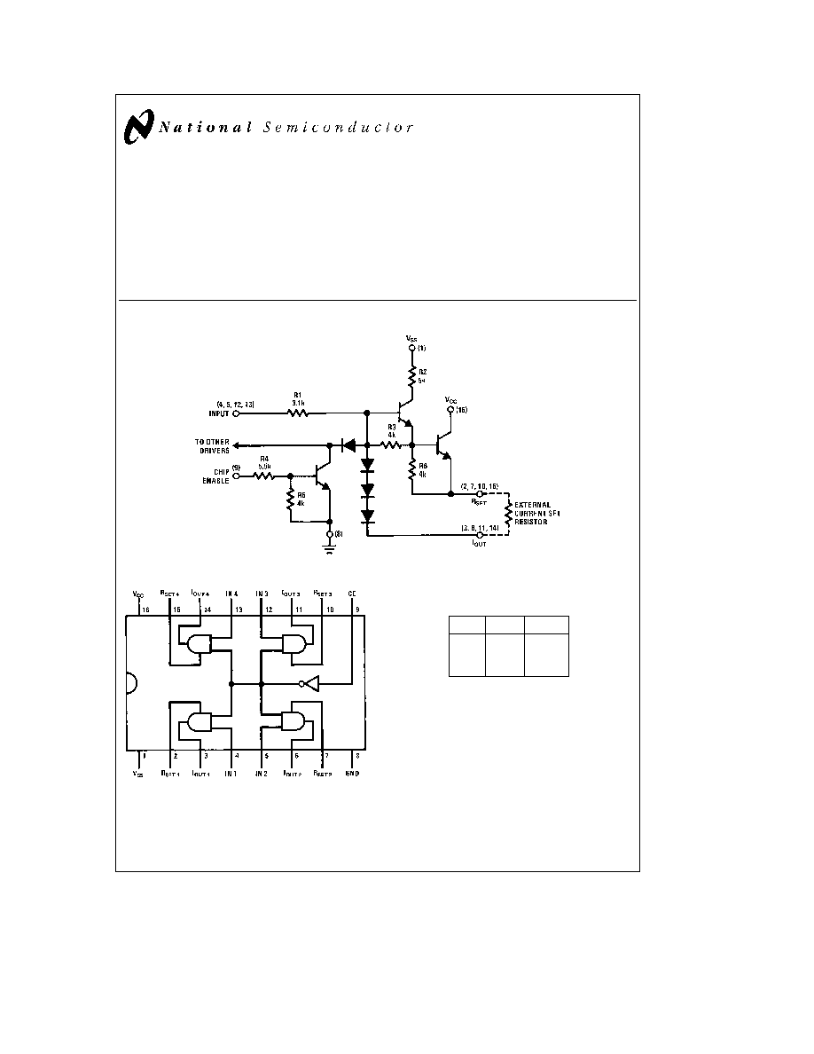
Schematic and Connection Diagrams
TL F 7561 ≠ 1
Dual-In-Line Package
TL F 7561 ≠ 2
Order Number DS55493J DS75493J
or DS75493N
See NS Package Number J16A or N16A
Truth Table
CE
V
IN
I
OUT
0
1
ON
0
0
OFF
1
X
OFF
X
e
Don't care
C1995 National Semiconductor Corporation
RRD-B30M105 Printed in U S A
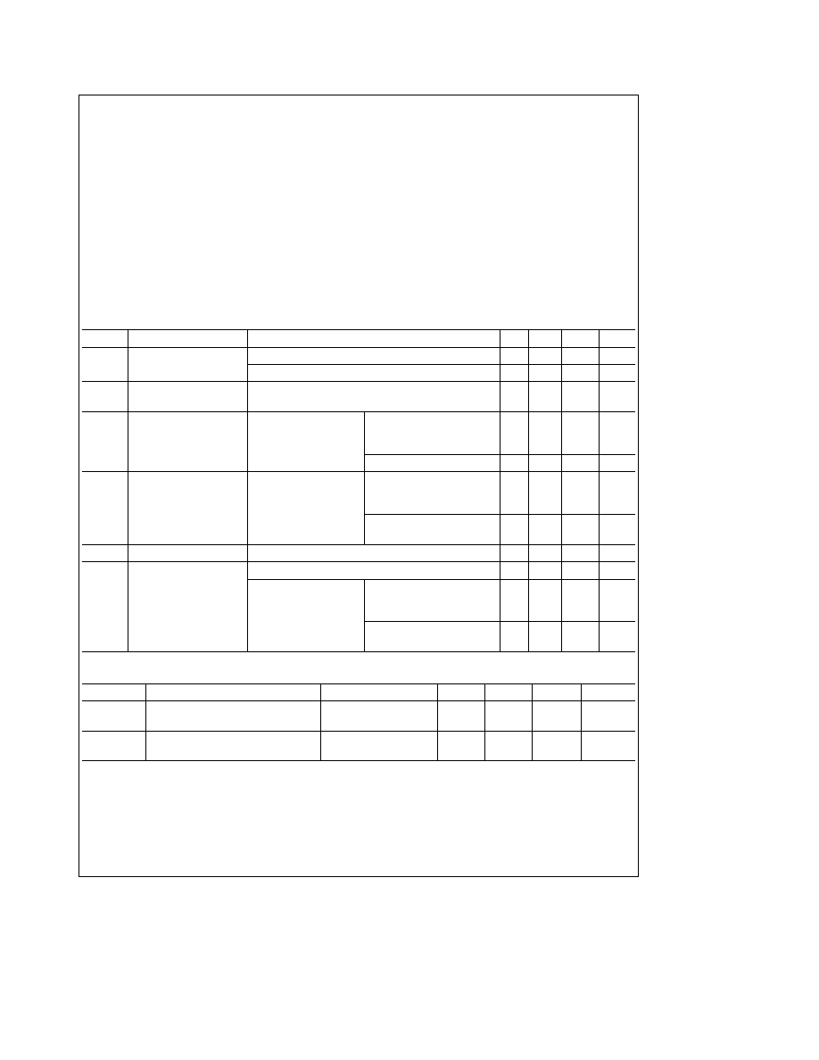
Absolute Maximum Ratings
(Note 1)
If Military Aerospace specified devices are required
please contact the National Semiconductor Sales
Office Distributors for availability and specifications
Supply Voltage
10V
Input Voltage
10V
Output Voltage
V
CC
Storage Temperature Range
b
65 C to
a
150 C
Output Current (I
OUT
)
b
25 mA
Maximum Power Dissipation at 25 C
Cavity Package
1371 mW
Molded Package
1280 mW
Lead Temperature (Soldering 4 seconds)
260 C
Derate cavity package 9 14 mW C above 25 C derate molded package
10 24 mW C above 25 C
Operating Conditions
Min
Max
Units
Supply Voltage
V
CC
3 2
8 8
V
V
SS
6 5
8 8
V
Temperature T
A
DS75493
0
a
70
C
DS55493
b
55
a
125
C
Electrical Characteristics
(V
SS
t
V
CC
) (Notes 2 and 3)
Symbol
Parameter
Conditions
Min
Typ
Max
Units
I
IN
Input Current
V
SS
e
Max V
IN
e
8 8V V
CC
e
Open V
CE
e
0V
3 2
mA
I
OUT
e
R
SET
0V V
CE
e
8 8V
3 6
mA
I
CE
Chip Enable Input Current
V
CC
e
Max V
SS
e
Max V
CE
e
8 8V All Other Pins
2 1
mA
to GND
I
OUT
Output Current
I
OUT
2 15V R
L
e
50X
V
CC
e
Min V
SS
e
6 5V
I
CE
e
80 mA V
IN
e
6 5V
b
8
b
13
mA
Through 1 0 kX
V
CE
e
0V V
IN
e
8 8V
b
16
b
20
mA
I
OL
Output Leakage Current
I
OUT
e
R
SET
0V
V
CC
e
Min V
CE
e
0V
Measure Current to Gnd
V
IN
e
8 8V Through
b
200
m
A
V
SS
e
8 8V
100 kX
V
CE
e
6 5V Though
b
100
m
A
1 0 kX V
IN
e
8 8V
I
CC
Supply Current V
CC
V
CC
e
Max V
SS
e
Max All Other Pins to Gnd
40
m
A
I
SS
Supply Current
V
CC
e
0V All Other Pins to Gnd
40
m
A
V
CC
e
Min V
SS
e
8 8V
I
OUT
2 15V V
CE
e
8 8V
Through 100 kX
0 5
1 5
mA
R
L
e
50X
I
OUT
e
Open R
SET
e
Open
1 4
mA
V
CE
e
0V
Switching Characteristics
T
A
e
25 C nominal power supplies unless otherwise noted
Symbol
Parameter
Conditions
Min
Typ
Max
Units
t
pd(OFF)
Propagation Delay to a Logical ``0''
(See AC Test Circuit
170
300
ns
From Input to Output
t
pd(ON)
Propagation Delay to a Logical ``1''
(See AC Test Circuit)
11
100
ns
From Input to Output
Note 1
``Absolute Maximum Ratings'' are those values beyond which the safety of the device cannot be guaranteed They are not meant to imply that the devices
should be operated at these limits The table of ``Electrical Characteristics'' provides conditions for actual device operation
Note 2
Unless otherwise specified min max limits apply across the 0 C to
a
70 C range for the DS75493 and across the
b
55 C to
a
125 C range for the
DS55493
Note 3
All currents into device pins shown as positive out of device pins as negative all voltages referenced to ground unless otherwise noted All values shown
as max or min on absolute value basis
2
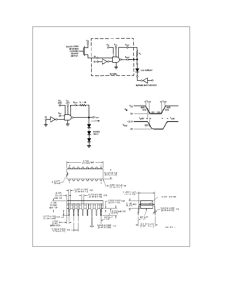
Typical Applications
TL F 7561 ≠ 3
AC Test Circuit
TL F 7561 ≠ 4
Switching Time Waveforms
TL F 7561 ≠ 5
Physical Dimensions
inches (millimeters)
Order Number DS55493J DS75493J
NS Package Number J16A
3

DS55493DS75493
Quad
LED
Segment
Driver
Physical Dimensions
inches (millimeters) (Continued)
Order Number DS75493N
See NS Package Number N16A
LIFE SUPPORT POLICY
NATIONAL'S PRODUCTS ARE NOT AUTHORIZED FOR USE AS CRITICAL COMPONENTS IN LIFE SUPPORT
DEVICES OR SYSTEMS WITHOUT THE EXPRESS WRITTEN APPROVAL OF THE PRESIDENT OF NATIONAL
SEMICONDUCTOR CORPORATION As used herein
1 Life support devices or systems are devices or
2 A critical component is any component of a life
systems which (a) are intended for surgical implant
support device or system whose failure to perform can
into the body or (b) support or sustain life and whose
be reasonably expected to cause the failure of the life
failure to perform when properly used in accordance
support device or system or to affect its safety or
with instructions for use provided in the labeling can
effectiveness
be reasonably expected to result in a significant injury
to the user
National Semiconductor
National Semiconductor
National Semiconductor
National Semiconductor
Corporation
Europe
Hong Kong Ltd
Japan Ltd
1111 West Bardin Road
Fax (a49) 0-180-530 85 86
13th Floor Straight Block
Tel 81-043-299-2309
Arlington TX 76017
Email cnjwge tevm2 nsc com
Ocean Centre 5 Canton Rd
Fax 81-043-299-2408
Tel 1(800) 272-9959
Deutsch Tel (a49) 0-180-530 85 85
Tsimshatsui Kowloon
Fax 1(800) 737-7018
English
Tel (a49) 0-180-532 78 32
Hong Kong
Fran ais Tel (a49) 0-180-532 93 58
Tel (852) 2737-1600
Italiano
Tel (a49) 0-180-534 16 80
Fax (852) 2736-9960
National does not assume any responsibility for use of any circuitry described no circuit patent licenses are implied and National reserves the right at any time without notice to change said circuitry and specifications