 | –≠–ª–µ–∫—Ç—Ä–æ–Ω–Ω—ã–π –∫–æ–º–ø–æ–Ω–µ–Ω—Ç: DS75115 | –°–∫–∞—á–∞—Ç—å:  PDF PDF  ZIP ZIP |
TL F 5787
DS75115DS9615
Dual
Differential
Line
Receiver
January 1996
DS75115 DS9615 Dual Differential Line Receiver
General Description
The DS75115 DS9615 is a dual differential line receiver de-
signed to sense differential signals from data transmission
lines Designed for operation over military and commercial
temperature ranges the DS75115 DS9615 can typically re-
ceive
g
500 mV differential data with
g
15V common-mode
noise Outputs are open-collector and give TTL compatible
signals which are a function of the polarity of the differential
input signal Active output pull-ups are also available offer-
ing the option of an active TTL pull-up through an external
connection
Response time may be controlled with the use of an exter-
nal capacitor Each channel may be independently con-
trolled and optional input termination resistors are also
available
Features
Y
Single 5V supply
Y
High common-mode voltage range
Y
Each channel individually strobed
Y
Independent response time control
Y
Uncommitted collector or active pull-up option
Y
TTL compatible output
Y
Optional 130X termination resistors
Y
Direct replacement for 9615
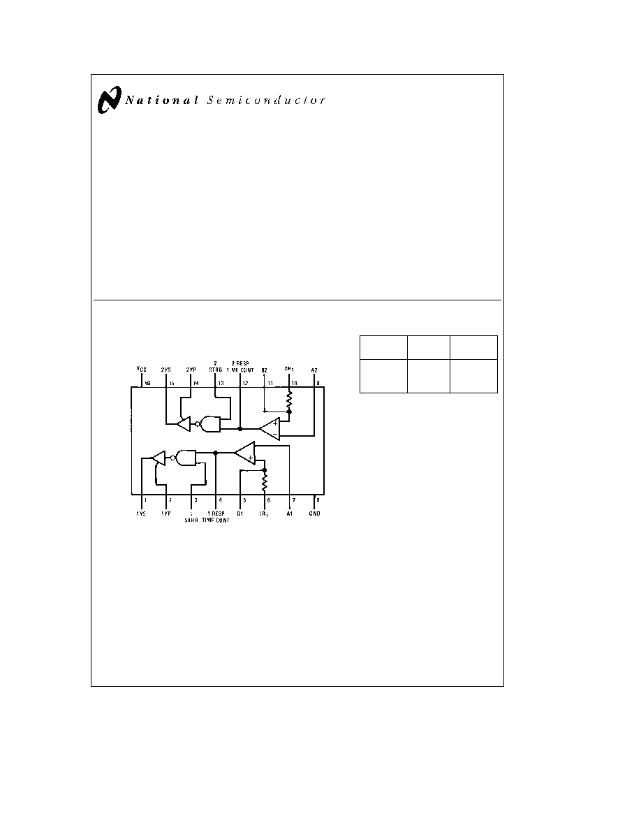
Connection Diagram
Dual-In-Line Package
TL F 5787 ≠ 1
Top View
Order Number DS75115N
See NS Package Number N16A
For Complete Military 883 Specifications See RETS Datasheet
Order Number DS9615MJ 883 DS9615ME 883
Function Table
Strobe
Diff
Output
Input
L
X
H
H
L
H
H
H
L
H
e
V
I
t
V
IH
min or V
ID
more positive than V
TH
max
L
e
V
I
s
V
IL
max or V
ID
more negative than V
TL
max
X
e
irrelevant
C1996 National Semiconductor Corporation
RRD-B30M36 Printed in U S A
http
www national com
Absolute Maximum Ratings
(Note 1)
If Military Aerospace specified devices are required
please contact the National Semiconductor Sales
Office Distributors for availability and specifications
Supply Voltage V
CC
(Note 1)
7V
Input Voltage at A B and R
T
Inputs
g
25V
Input Voltage at Strobe Input
5 5V
Off-State Voltage Applied to Open-Collector Outputs
14V
Maximum Power Dissipation at 25 C
Cavity Package
1433 mW
Molded Package
1362 mW
Operating Free-Air Temperature Range
DS9615M
b
55 C to
a
125 C
DS57115
0 C to
a
70 C
Storage Temperature Range
b
65 C to
a
150 C
Lead Temperature
(
inch from case for 4 seconds)
260 C
Derate cavity package 9 6 mW C above 25 C derate molded package
10 9 mW C above 25 C
Operating Conditions
Min
Max
Units
Supply Voltage (V
CC
)
DS9615M
4 5
5 5
V
DS75115
4 75
5 25
V
High Level Output Current (I
OH
)
b
5
mA
Low Level Output Current (I
OL
)
15
mA
Operating Temperature (T
A
)
DS9615M
b
55
125
C
DS75115
0
70
C
Electrical Characteristics
(Notes 2 3 and 5)
Symbol
Parameter
Conditions
DS75115
Units
Min
Typ
Max
V
TH
Differential Input High-
V
O
e
0 4V I
OL
e
15 mA V
IC
e
0V
200
500
mV
Threshold Voltage
V
TL
Differential Input Low-
V
O
e
2 4V I
OH
e b
5 mA V
IC
e
0V
b
200
b
500
mV
Threshold Voltage
V
ICR
Common-Mode Input
V
ID
e
g
1V
15
24
Voltage Range
to
to
V
b
15
b
19
V
IH(STROBE)
High-Level Strobe
2 4
V
Input Voltage
V
IL(STROBE)
Low-Level Strobe
0 4
V
Input Voltage
V
OH
High Level Output Voltage
V
CC
e
Min V
ID
e b
0 5V
T
A
e
Min
2 4
I
OH
e b
5 mA
T
A
e
25 C
2 4
3 4
V
T
A
e
Max
2 4
V
OL
Low Level Output Voltage
V
CC
e
Min V
ID
e
0 5V I
OL
e
15 mA
0 22
0 45
V
I
IL
Low Level Input Current
V
CC
e
Max V
I
e
0 4V
T
A
e
Min
b
0 9
Other Input at 5 5V
T
A
e
25 C
b
0 5
b
0 7
mA
T
A
e
Max
b
0 7
I
SH
High Level Strobe Current
V
CC
e
Min V
ID
e b
0 5V
T
A
e
25 C
0 5
5
m
A
V
STROBE
e
4 5V
T
A
e
Max
10
I
SL
Low Level Strobe Current
V
CC
e
Max V
ID
e
0 5V
T
A
e
25 C
b
1 15
b
2 4
mA
V
STROBE
e
0 4V
I
4
I
12
Response Time Control
V
CC
e
Max V
ID
e
0 5V
T
A
e
25 C
b
1 2
b
3 4
mA
Current (Pin 4 or Pin 12)
V
RC
e
0V
I
O(OFF)
Off-State Open-Collector
V
CC
e
Min V
OH
e
12V
T
A
e
25 C
Output Current
V
ID
e b
4 5V
T
A
e
Max
m
A
V
CC
e
Min V
OH
e
5 25V
T
A
e
25 C
100
V
ID
e b
4 75V
T
A
e
Max
200
http
www national com
2
Electrical Characteristics
(Notes 2 3 and 5) (Continued)
Symbol
Parameter
Conditions
DS75115
Units
Min
Typ
Max
R
T
Line Terminating
V
CC
e
5V
T
A
e
25 C
74
130
179
X
Resistance
I
OS
Short-Circuit Output
V
CC
e
Max V
O
e
0V
T
A
e
25 C
b
14
b
40
b
100
mA
Current
V
ID
e b
0 5V (Note 4)
I
CC
Supply Current (Both
V
CC
e
Max V
ID
e
0 5V
T
A
e
25 C
32
50
mA
Receivers)
V
IC
e
0V
Note 1
``Absolute Maximum Ratings'' are those values beyond which the safety of the device cannot be guaranteed Except for ``Operating Temperature Range''
they are not meant to imply that the devices should be operated at these limits The table of ``Electrical Characteristics'' provides conditions for the actual device
operation
Note 2
Unless otherwise specified min max limits apply across the
b
55 C to
a
125 C temperature range for the DS9615M and across the 0 C to
a
70 C range for
the DS75115 All typical values are for T
A
e
25 C V
CC
e
5V and V
CM
e
0V
Note 3
All currents into device pins shown as positive out of device pins as negative all voltages referenced to ground unless otherwise noted All values shown
as max or min on absolute value basis
Note 4
Only one output at a time should be shorted
Note 5
Unless otherwise noted V
STROBE
e
2 4V All parameters with the exception of off-state open-collector output current are measured with the active pull-up
connected to the sink output
Switching Characteristics
V
CC
e
5V C
L
e
30 pF T
A
e
25 C
Symbol
Parameter
Conditions
DS75115
Units
Min
Typ
Max
t
PLH
Propagation Delay Time Low-
R
L
e
3 9 kX
(Figure 1)
18
75
ns
to-High Level Output
t
PHL
Propagation Delay Time High-
R
L
e
390X
(Figure 1)
20
75
ns
to-Low Level Output
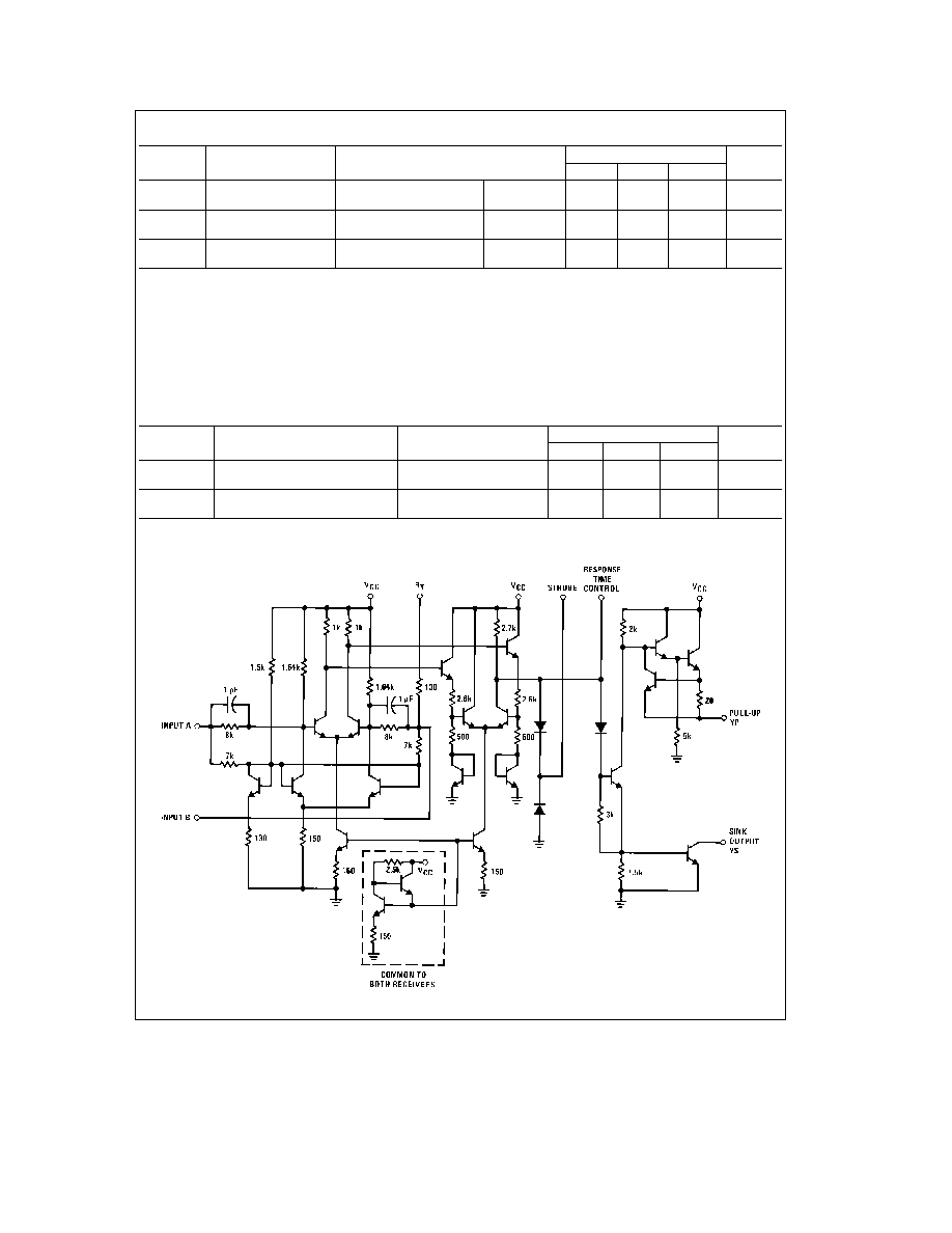
Schematic Diagram
TL F 5787 ≠ 2
http
www national com
3
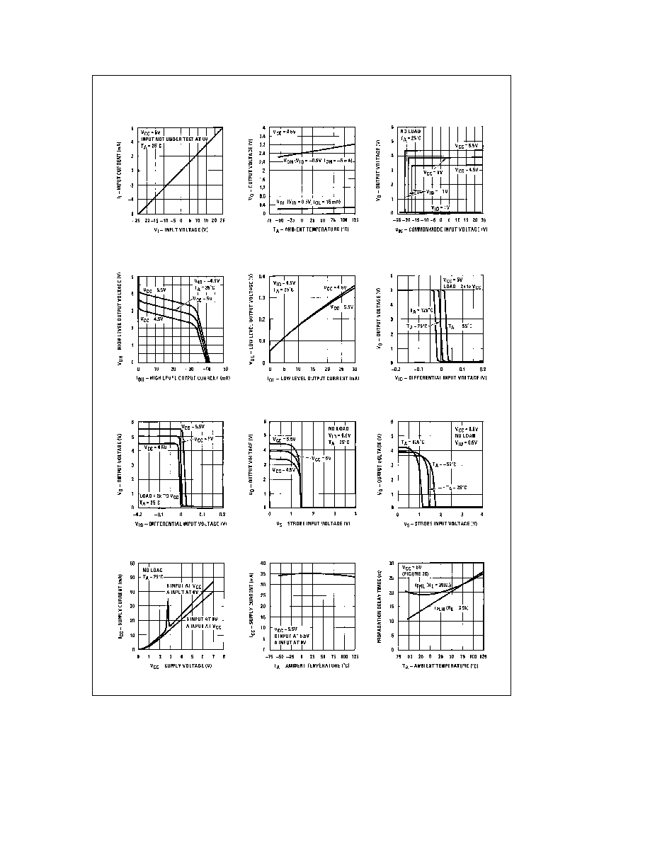
Typical Performance Characteristics
(Note 3)
Voltage
Input Current vs Input
Temperature
Output Voltage vs
Input Voltage
Common-Mode
Output Voltage vs
vs Output Current
High Level Output Voltage
vs Output Current
Low Level Output Voltage
Differential Input Voltage
Output Voltage vs
vs Differential Input Voltage
Output Voltage
Strobe Input Voltage
Output Voltage vs
Strobe Input Voltage
Output Voltage vs
vs Supply Voltage
Supply Current (Both Receivers)
vs Temperature
Supply Current (Both Receivers)
vs Temperature
Propagation Delay Times
TL F 5787 ≠ 4
http
www national com
4
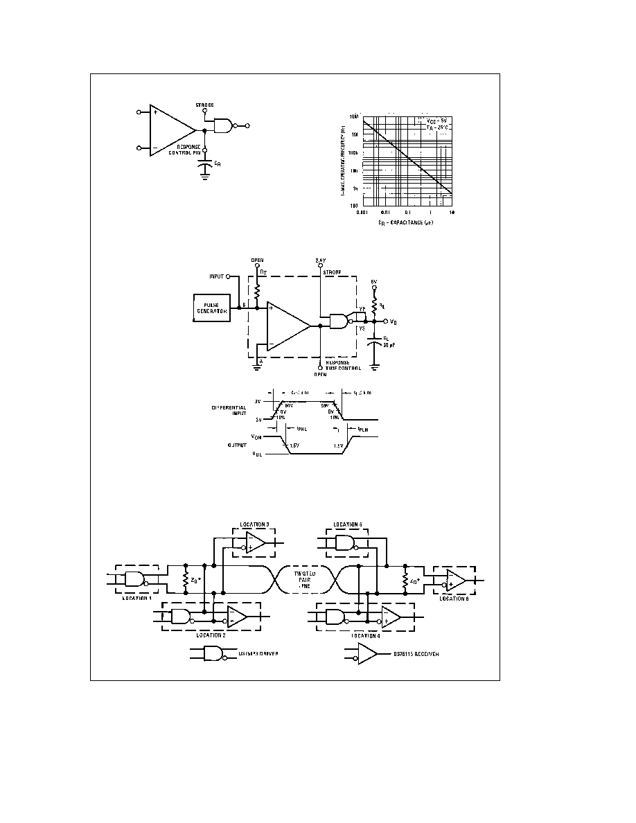
Frequency Response Control
TL F 5787 ≠ 5
Note
C
R
(response control)
l
0 01 mF may cause slowing of rise and fall
times of the output
Frequency Response as a
Function of Capacitance
TL F 5787 ≠ 6
AC Test Circuit and Switching Time Waveforms
TL F 5787 ≠ 7
TL F 5787 ≠ 8
FIGURE 1 Propagation Delay Time (Notes 1 2)
Note 1
The pulse generator has the following characteristics Z
OUT
e
50X PRR
e
500 kHz t
W
e
100 ns
Note 2
C
L
includes probe and test fixture capacitance
Typical Application
Basic Party-Line or Data-Bus Differential Data Transmission
Z
O
is internal to the DS9615 DS75115
TL F 5787 ≠ 3
A capacitor may be connected in series with Z
O
to reduce power dissipation
http
www national com
5