 | –≠–ª–µ–∫—Ç—Ä–æ–Ω–Ω—ã–π –∫–æ–º–ø–æ–Ω–µ–Ω—Ç: DS75124 | –°–∫–∞—á–∞—Ç—å:  PDF PDF  ZIP ZIP |

TL F 5792
DS75124
Triple
Line
Receiver
February 1996
DS75124 Triple Line Receiver
General Description
The DS75124 is designed to meet the input output interface
specifications for IBM System 360 It has built-in hysteresis
on one input on each of the three receivers to provide large
noise margin The other inputs on each receiver are in a
standard TTL configuration The DS75124 is compatible
with standard TTL logic and supply voltage levels
Features
Y
Built-in input threshold hysteresis
Y
High speed
typical propagation delay time 20 ns
Y
Independent channel strobes
Y
Input gating increases application flexibility
Y
Single 5 0V supply operation
Y
Plug-in replacement for the SN75124 and the 8T24
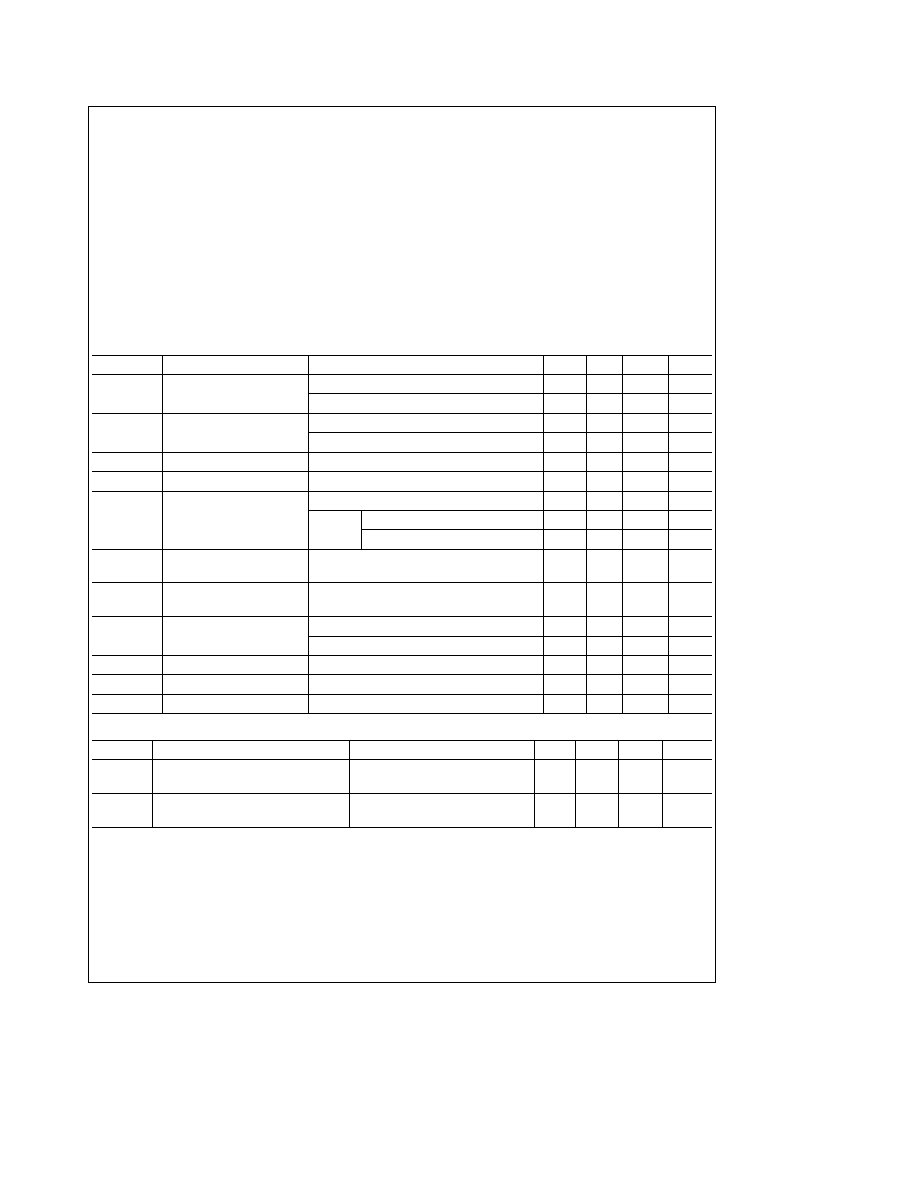
Connection Diagram and Truth Table
Dual-In-Line Package
TL F 5792 ≠ 1
Top View
Order Number DS75124N
See NS Package Number N16A
Inputs
Output
A
B
R
S
Y
H
H
X
X
L
X
X
L
H
L
L
X
H
X
H
L
X
X
L
H
X
L
H
X
H
X
L
X
L
H
H
e
high level L
e
low level X
e
irrelevant
B input and last two lines of the truth table
are applicable to receivers 1 and 2 only
Typical Application
TL F 5792 ≠ 2
C1996 National Semiconductor Corporation
RRD-B30M36 Printed in U S A
http
www national com
Absolute Maximum Ratings
(Note 1)
If Military Aerospace specified devices are required
please contact the National Semiconductor Sales
Office Distributors for availability and specifications
Supply Voltage V
CC
7 0V
Input Voltage
R Input with V
CC
Applied
7 0V
R Input with V
CC
not Applied
6 0V
A B or S Input
5 5V
Output Voltage
7 0V
Output Current
g
100 mA
Maximum Power Dissipation at 25 C
Molded Package
1362 mW
Operating Temperature Range
0 C to
a
75 C
Storage Temperature Range
b
65 C to
a
150 C
Lead Temperature (Soldering 4 seconds)
260 C
Derate molded package 10 9 mW C above 25 C
Operating Conditions
Min
Max
Units
Supply Voltage V
CC
4 75
5 25
V
High Level Output Current
b
800
m
A
I
OH
Low Level Output Current
16
mA
I
OL
Operating Temperature T
A
0
a
75
C
Electrical Characteristics
(Notes 2 and 3)
Symbol
Parameter
Conditions
Min
Typ
Max
Units
V
IH
High Level Input Voltage
A B or S
2 0
V
R
1 7
V
V
IL
Low Level Input Voltage
A B or S
0 8
V
R
0 8
V
V
Ta
b
V
Tb
Hysteresis
V
CC
e
5 0V T
A
e
25 C R (Note 6)
0 2
0 4
V
V
I
Input Clamp Voltage
V
CC
e
5 0V I
I
e b
12 mA A B or S
b
1 5
V
I
I
Input Current at Maximum
V
CC
e
5 25V V
IN
e
5 5V A B or S
1
mA
Input Voltage
R
V
I
e
7 0V
5 0
mA
V
I
e
6 0V V
CC
e
0V
5 0
mA
V
OH
High Level Output Voltage
V
IH
e
V
IHMIN
V
IL
e
V
ILMAX
2 6
V
I
OH
e b
800 mA (Note 4)
V
OL
Low Level Output Voltage
V
IH
e
V
IHMIN
V
IL
e
V
ILMAX
I
OL
e
16 mA
0 4
V
(Note 4)
I
IH
High Level Input Current
V
I
e
4 5V A B or S
40
m
A
V
I
e
3 11V R
170
m
A
I
IL
Low Level Input Current
V
I
e
0 4V A B or S
b
0 1
b
1 6
mA
I
OS
Short Circuit Output Current
V
CC
e
5 0V T
A
e
25 C (Note 5)
b
50
b
100
mA
I
CC
Supply Current
V
CC
e
5 25V
72
mA
Switching Characteristics
T
A
e
25 C nominal power supplies unless otherwise noted
Symbol
Parameter
Conditions
Min
Typ
Max
Units
t
PLH
Propagation Delay Time Low-to-High
(See AC Test Circuit and Switching
20
30
ns
Level Output from R Input
Time Waveforms)
t
PHL
Propagation Delay Time High-to-Low
(See AC Test Circuit and Switching
20
30
ns
Level Output from R Input
Time Waveforms)
Note 1
``Absolute Maximum Ratings'' are those values beyond which the safety of the device cannot be guaranteed Except for ``Operating Temperature Range''
they are not meant to imply that the devices should be operated at these limits The table of ``Electrical Characteristics'' provides conditions for actual device
operation
Note 2
All currents into device pins are shown as positive currents out of device pins shown as negative all voltage values are referenced with respect to network
ground terminal unless otherwise noted All values shown as max or min on absolute value basis
Note 3
Min max limits apply across the guaranteed operating temperature range of 0 C to
a
75 C for DS75124 unless otherwise specified Typicals are for V
CC
e
5 0V T
A
e
25 C Positive current is defined as current into the referenced pin
Note 4
The output voltage and current limits are guaranteed for any appropriate combination of high and low inputs specified by the truth table for the desired
output
Note 5
Not more than one output should be shorted at a time
Note 6
Hysteresis is the difference between the positive going input threshold voltage V
T
a
and the negative going input threshold voltage V
T
b
http
www national com
2
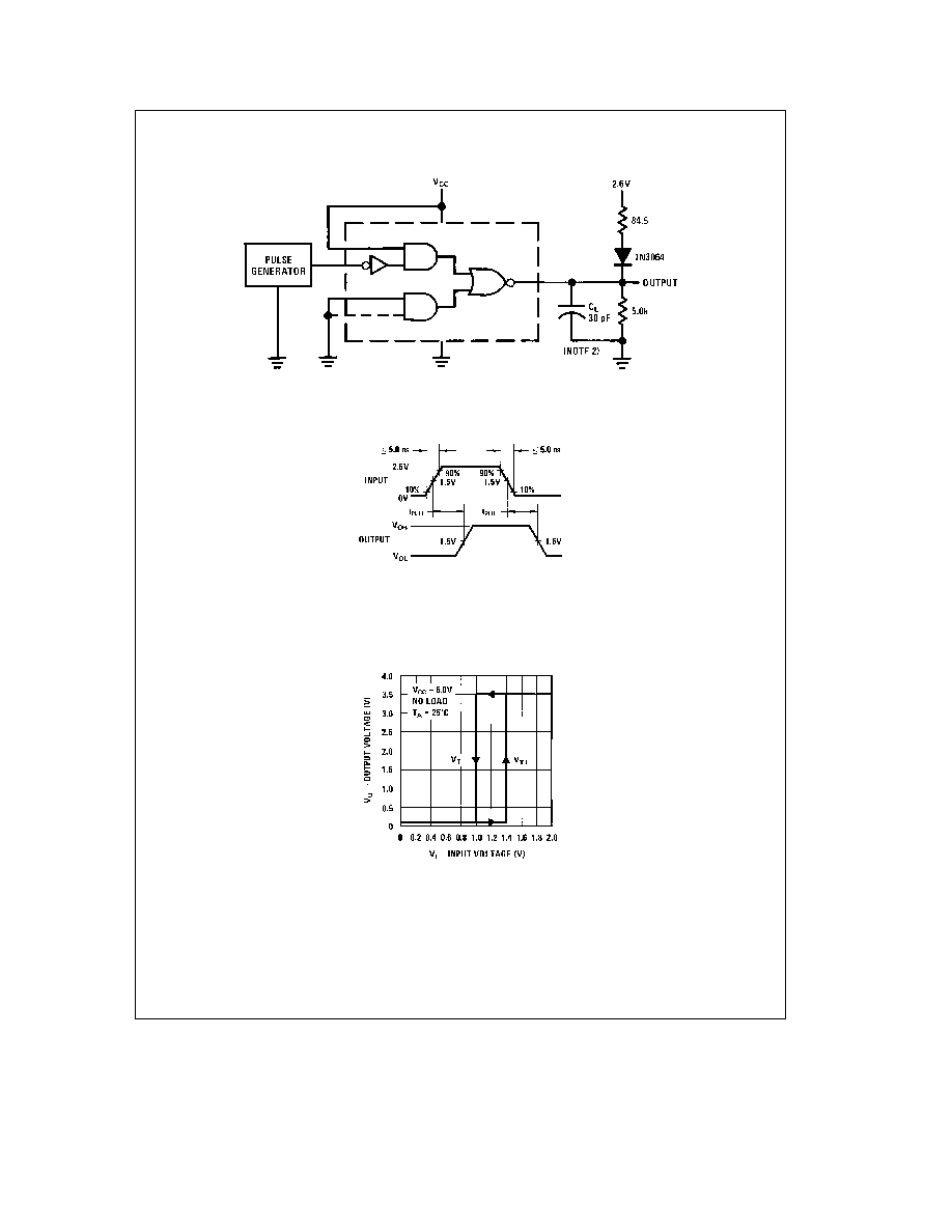
AC Test Circuit and Switching Time Waveforms
TL F 5792 ≠ 3
Note 1
The pulse generator has the following characteristics Z
OUT
50X t
W
e
200 ns duty cycle
e
50%
Note 2
C
L
includes probe and jig capacitance
TL F 5792 ≠ 4
Typical Performance Characteristics
Output Voltage vs
Receiver Input Voltage
TL F 5792 ≠ 5
http
www national com
3

DS75124
Triple
Line
Receiver
Physical Dimensions
inches (millimeters)
Molded Dual-In-Line Package (N)
Order Number DS75124N
NS Package Number N16A
LIFE SUPPORT POLICY
NATIONAL'S PRODUCTS ARE NOT AUTHORIZED FOR USE AS CRITICAL COMPONENTS IN LIFE SUPPORT
DEVICES OR SYSTEMS WITHOUT THE EXPRESS WRITTEN APPROVAL OF THE PRESIDENT OF NATIONAL
SEMICONDUCTOR CORPORATION As used herein
1 Life support devices or systems are devices or
2 A critical component is any component of a life
systems which (a) are intended for surgical implant
support device or system whose failure to perform can
into the body or (b) support or sustain life and whose
be reasonably expected to cause the failure of the life
failure to perform when properly used in accordance
support device or system or to affect its safety or
with instructions for use provided in the labeling can
effectiveness
be reasonably expected to result in a significant injury
to the user
National Semiconductor
National Semiconductor
National Semiconductor
National Semiconductor
Corporation
Europe
Hong Kong Ltd
Japan Ltd
1111 West Bardin Road
Fax a49 (0) 180-530 85 86
13th Floor Straight Block
Tel 81-043-299-2308
Arlington TX 76017
Email europe support nsc com
Ocean Centre 5 Canton Rd
Fax 81-043-299-2408
Tel 1(800) 272-9959
Deutsch Tel a49 (0) 180-530 85 85
Tsimshatsui Kowloon
Fax 1(800) 737-7018
English
Tel a49 (0) 180-532 78 32
Hong Kong
Fran ais Tel a49 (0) 180-532 93 58
Tel (852) 2737-1600
http
www national com
Italiano
Tel a49 (0) 180-534 16 80
Fax (852) 2736-9960
National does not assume any responsibility for use of any circuitry described no circuit patent licenses are implied and National reserves the right at any time without notice to change said circuitry and specifications