 | –≠–ª–µ–∫—Ç—Ä–æ–Ω–Ω—ã–π –∫–æ–º–ø–æ–Ω–µ–Ω—Ç: DS75150 | –°–∫–∞—á–∞—Ç—å:  PDF PDF  ZIP ZIP |
DS75150
Dual Line Driver
General Description
The DS75150 is a dual monolithic line driver designed to sat-
isfy the requirements of the standard interface between data
terminal equipment and data communication equipment as
defined by EIA Standard RS-232-C. A rate of 20,000 bits per
second can be transmitted with a full 2500 pF load. Other ap-
plications are in data-transmission systems using relatively
short single lines, in level translators, and for driving MOS
devices. The logic input is compatible with most TTL and LS
families. Operation is from -12V and +12V power supplies.
Features
n
Withstands sustained output short-circuit to any low
impedance voltage between -25V and +25V
n
2 µs max transition time through the -3V to +3V
transition region under full 2500 pF load
n
Inputs compatible with most TTL and LS families
n
Common strobe input
n
Inverting output
n
Slew rate can be controlled with an external capacitor at
the output
n
Standard supply voltages:
±
12V
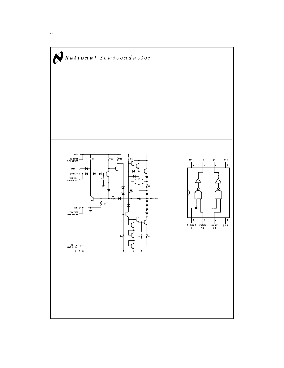
Schematic and Connection Diagrams
DS005794-1
Component values shown are nominal.
1/2 of circuit shown
Dual-In-Line Package
DS005794-2
Positive Logic C = AS
Top View
Order Number DS75150M
See NS Package Number M08A
May 1998
DS75150
Dual
Line
Driver
© 1998 National Semiconductor Corporation
DS005794
www.national.com
Absolute Maximum Ratings
(Note 2)
If Military/Aerospace specified devices are required,
please contact the National Semiconductor Sales Office/
Distributors for availability and specifications.
Supply Voltage +V
CC
15V
Supply Voltage -V
CC
15V
Input Voltage
15V
Applied Output Voltage
+25V
Storage Temperature Range
-65∞C to +150∞C
Maximum Power Dissipation (Note 1) at 25∞C
SO Package
655 mW
Lead Temperature (Soldering, 4
sec.)
260∞C
Operating Conditions
Min
Max
Units
Supply Voltage (+V
CC
)
10.8
13.2
V
Supply Voltage (-V
CC
)
-10.8
-13.2
V
Input Voltage (V
I
)
0
+5.5
V
Output Voltage (V
O
)
±
15
V
Operating Ambient Temperature
Range (T
A
)
0
+70
∞C
Note 1: Derate SO package 8.01 mW/∞C above 25∞C.
DC Electrical Characteristics
(Notes 3, 4, 5, 6)
Symbol
Parameter
Conditions
Min
Typ
Max
Units
V
IH
High-Level Input Voltage
(Figure 1 )
2
V
V
IL
Low-Level Input Voltage
(
Figure 2)
0.8
V
V
OH
High-Level Output Voltage
+V
CC
= 10.8V,-V
CC
= -13.2V, V
IL
= 0.8V,
5
8
V
R
L
= 3 k
to 7 k
(
Figure 2)
V
OL
Low-Level Output Voltage
+V
CC
= 10.8V,-V
CC
= -10.8V, V
IH
= 2V,
-8
-5
V
R
L
= 3 k
to 7 k
(
Figure 1)
I
IH
High-Level Input Current
+V
CC
= 13.2V,-V
CC
= -13.2V,
Data Input
1
10
µA
V
I
= 2.4V, (Figure 3)
+V
CC
= 13.2V, -V
CC
= -13.2V,
Strobe Input
2
20
µA
V
I
= 2.4V, (Figure 3)
I
IL
Low-Level Input Current
+V
CC
= 13.2V,-V
CC
= -13.2V,
Data Input
-1
-1.6
mA
V
I
= 0.4V, (Figure 3)
+V
CC
= 13.2V, -V
CC
= -13.2V,
Strobe Input
-2
-3.2
mA
V
I
= 0.4V, (Figure 3)
I
OS
Short-Circuit Output Current
+V
CC
= 13.2V,-V
CC
= -13.2V,
V
O
= 25V
2
5
mA
(
Figure 4), (Note 5)
V
O
= -25V
-3
-6
mA
V
O
= 0V, V
I
= 3V
15
30
mA
V
O
= 0V, V
I
= 0V
-15
-30
mA
+I
CCH
Supply Current From +V
CC
,
+V
CC
= 13.2V, -V
CC
= -13.2V, V
I
= 0V,
10
22
mA
High-Level Output
R
L
= 3 k
, T
A
= 25∞C, (Figure 5)
-I
CCH
Supply Current From -V
CC
,
+V
CC
= 13.2V, -V
CC
= -13.2V, V
I
= 0V,
-1
-10
mA
High-Level Output
R
L
= 3 k
, T
A
= 25∞C, (Figure 5)
+I
CCL
Supply Current From +V
CC
,
+V
CC
= 13.2V, -V
CC
= -13.2V, V
I
= 3V,
8
17
mA
Low-Level Output
R
L
= 3 k
, T
A
= 25∞C, (Figure 5)
-I
CCL
Supply Current From -V
CC
,
+V
CC
= 13.2V, -V
CC
= -13.2V, V
I
= 3V,
-9
-20
mA
Low-Level Output
R
L
= 3 k
, T
A
= 25∞C, (Figure 5)
Note 2: "Absolute Maximum Ratings" are those values beyond which the safety of the device cannot be guaranteed. Except for "Operating Temperature Range" they
are not meant to imply that the devices should be operated at these limits. The table of "Electrical Characteristics" provides conditions for actual device operation.
Note 3: Unless otherwise specified min/max limits apply across the 0∞C to +70∞C range for the DS75150. All typical values are T
A
= 25∞C and +V
CC
= 12V, -V
CC
= -12V.
Note 4: All current into device pins shown as positive, out of device pins as negative, all voltages referenced to ground unless otherwise noted. All values shown
as max or min on absolute value basis.
Note 5: Only one output at a time should be shorted.
Note 6: The algebraic convention where the most-positive (least-negative) limit is designated as maximum is used in this data sheet for logic levels only, e.g., when
-5V is the maximum, the typical value is more-negative voltage.
www.national.com
2
AC Electrical Characteristics
(+V
CC
= 12V, -V
CC
= -12V, T
A
= 25∞C)
Symbol
Parameter
Conditions
Min
Typ
Max
Units
t
TLH
Transition Time, Low-to-High
C
L
= 2500 pF, R
L
= 3 k
to 7 k
,
0.2
1.4
2
µs
Level Output
(
Figure 6)
t
THL
Transition Time, High-to-Low
C
L
= 2500 pF, R
L
= 3 k
to 7 k
,
0.2
1.5
2
µs
Level Output
(
Figure 6)
t
TLH
Transition Time, Low-to-High
C
L
= 15 pF, R
L
= 7 k
, (
Figure 6)
40
ns
Level Output
t
THL
Transition Time, High-to-Low
C
L
= 15 pF, R
L
= 7 k
, (
Figure 6)
20
ns
Level Output
t
PLH
Propagation Delay Time
C
L
= 15 pF, R
L
= 7 k
, (
Figure 6)
60
ns
Low-to-High Level Output
t
PHL
Propagation Delay Time
C
L
= 15 pF, R
L
= 7 k
, (
Figure 6)
45
ns
High-to-Low Level Output
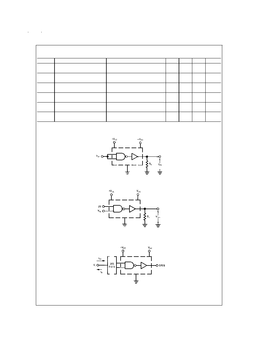
DC Test Circuits
DS005794-3
FIGURE 1. V
IH
, V
OL
DS005794-4
Each input is tested separately.
FIGURE 2. V
IL
, V
OH
DS005794-5
When testing I
IH
, the other input is at 3V; when testing I
IL
, the other input is open.
FIGURE 3. I
IH
, I
IL
www.national.com
3
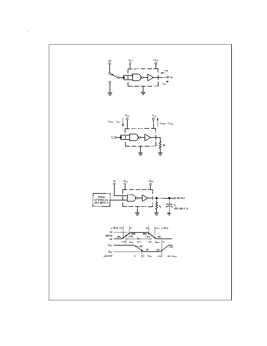
DC Test Circuits
(Continued)
AC Test Circuit and Switching Waveforms
DS005794-6
I
OS
is tested for both input conditions at each of the specified output conditions.
FIGURE 4. I
OS
DS005794-7
FIGURE 5. I
CCH+
, I
CCH-
, I
CCL+
, I
CCL-
DS005794-8
DS005794-9
Note 7: The pulse generator has the following characterstics:
duty cycle
50%, Z
OUT
50
.
Note 8: C
L
includes probe and jig capacitance.
FIGURE 6.
www.national.com
4
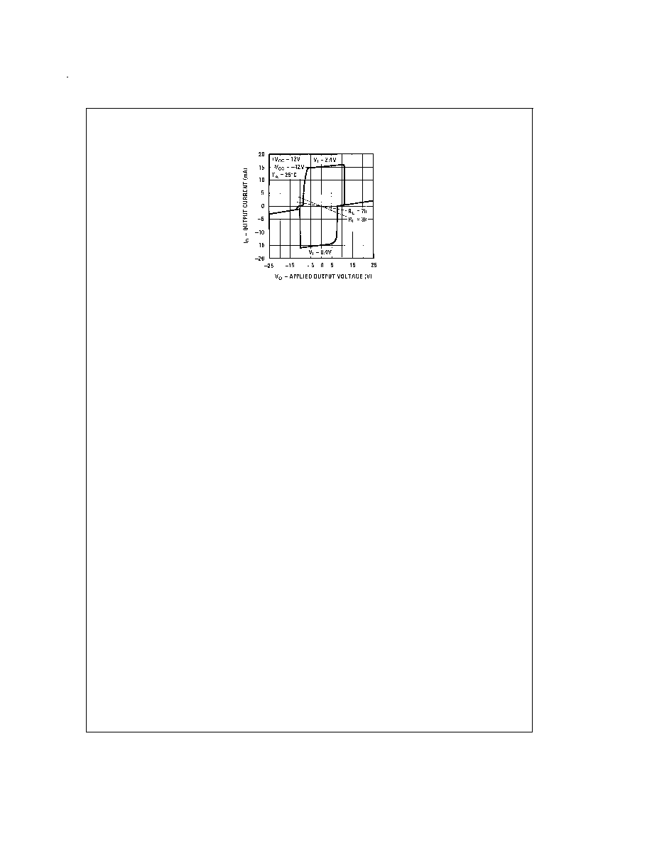
Typical Performance Characteristics
Output Current vs Applied Output Voltage
DS005794-10
FIGURE 7.
www.national.com
5
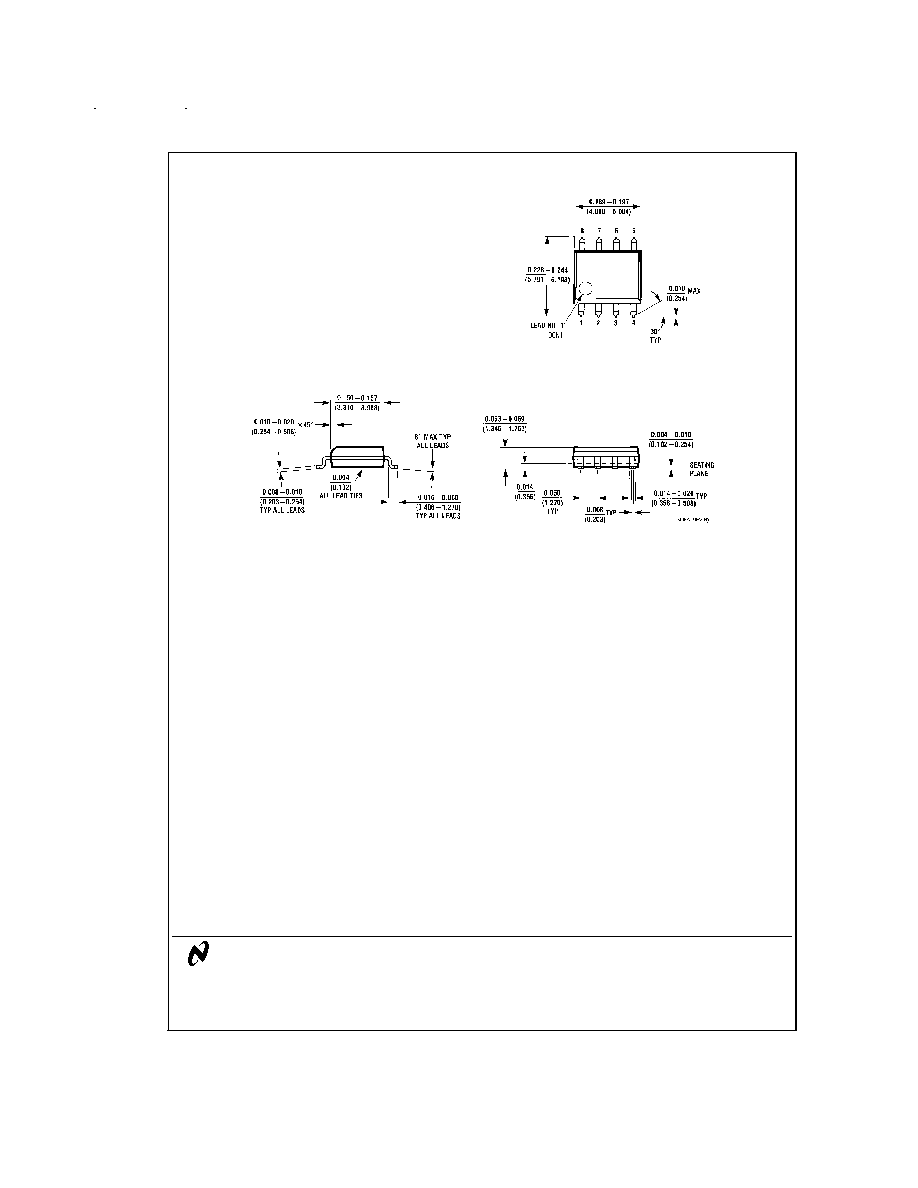
Physical Dimensions
inches (millimeters) unless otherwise noted
LIFE SUPPORT POLICY
NATIONAL'S PRODUCTS ARE NOT AUTHORIZED FOR USE AS CRITICAL COMPONENTS IN LIFE SUPPORT DE-
VICES OR SYSTEMS WITHOUT THE EXPRESS WRITTEN APPROVAL OF THE PRESIDENT OF NATIONAL SEMI-
CONDUCTOR CORPORATION. As used herein:
1. Life support devices or systems are devices or sys-
tems which, (a) are intended for surgical implant into
the body, or (b) support or sustain life, and whose fail-
ure to perform when properly used in accordance
with instructions for use provided in the labeling, can
be reasonably expected to result in a significant injury
to the user.
2. A critical component in any component of a life support
device or system whose failure to perform can be rea-
sonably expected to cause the failure of the life support
device or system, or to affect its safety or effectiveness.
National Semiconductor
Corporation
Americas
Tel: 1-800-272-9959
Fax: 1-800-737-7018
Email: support@nsc.com
www.national.com
National Semiconductor
Europe
Fax: +49 (0) 1 80-530 85 86
Email: europe.support@nsc.com
Deutsch Tel: +49 (0) 1 80-530 85 85
English
Tel: +49 (0) 1 80-532 78 32
FranÁais Tel: +49 (0) 1 80-532 93 58
Italiano
Tel: +49 (0) 1 80-534 16 80
National Semiconductor
Asia Pacific Customer
Response Group
Tel: 65-2544466
Fax: 65-2504466
Email: sea.support@nsc.com
National Semiconductor
Japan Ltd.
Tel: 81-3-5620-6175
Fax: 81-3-5620-6179
SO Package (M)
Order Number DS75150M
NS Package Number M08A
DS75150
Dual
Line
Driver
National does not assume any responsibility for use of any circuitry described, no circuit patent licenses are implied and National reserves the right at any time without notice to change said circuitry and specifications.