TL F 9755
DS75325
Memory
Drivers
June 1992
DS75325
Memory Drivers
General Description
The DS75325 is a monolithic memory driver which features
high current outputs as well as internal decoding of logic
inputs This circuit is designed for use with magnetic memo-
ries
The circuit contains two 600 mA sink-switch pairs and two
600 mA source-switch pairs Inputs A and B determine
source selection while the source strobe (S1) allows the
selected source turn on In the same manner inputs C and
D determine sink selection while the sink strobe (S2) allows
the selected sink turn on
Sink-output collectors feature an internal pull-up resistor in
parallel with a clamping diode connected to V
CC2
This pro-
tects the outputs from voltage surges associated with
switching inductive loads
The source stage features Node R which allows extreme
flexibility in source current selection by controlling the
amount of base drive to each source transistor This method
of setting the base drive brings the power associated with
the resistor outside the package thereby allowing the circuit
to operate at higher source currents for a given junction
temperature If this method of source current setting is not
desired then Nodes R and R
INT
can be shorted externally
activating an internal resistor connected from V
CC2
to Node
R This provides adequate base drive for source currents up
to 375 mA with V
CC2
e
15V or 600 mA with V
CC2
e
24V
Features
Y
600 mA output capability
Y
24V output capability
Y
Dual sink and dual source outputs
Y
Fast switching times
Y
Source base drive externally adjustable
Y
Input clamping diodes
Y
TTL compatible
Connection Diagram
Dual-In-Line Package
TL F 9755 ≠ 2
Top View
Order Number DS75325N
See NS Package Number N14A
Truth Table
Address Inputs
Strobe Inputs
Outputs
Source
Sink
Source
Sink
Source
Sink
A
B
C
D
S1
S2
W
X
Y
Z
L
H
X
X
L
H
ON
OFF OFF OFF
H
L
X
X
L
H
OFF ON
OFF OFF
X
X
L
H
H
L
OFF OFF ON
OFF
X
X
H
L
H
L
OFF OFF OFF ON
X
X
X
X
H
H
OFF OFF OFF OFF
H
H
H
H
X
X
OFF OFF OFF OFF
H
e
High Level L
e
Low Level X
e
Irrelevant
Note
Not more than one output is to be on at any one time
C1995 National Semiconductor Corporation
RRD-B30M115 Printed in U S A

Absolute Maximum Ratings
(Note 1)
If Military Aerospace specified devices are required
please contact the National Semiconductor Sales
Office Distributors for availability and specifications
Supply Voltage V
CC1
(Note 5)
7V
Supply Voltage V
CC2
(Note 5)
25V
Input Voltage (Any Address or Strobe Input)
5 5V
Maximum Power Dissipation at 25 C
Cavity Package
1509 mW
Molded Package
1476 mW
Derate Cavity Package 10 1 mW C above 25 C derate molded package
11 8 mW C above 25 C
Storage Temperature Range
b
65 C to
a
150 C
Lead Temperature
(Soldering 10 seconds)
300 C
Operating Conditions
Min
Max
Units
Temperature (T
A
)
DS75325
0
a
70
C
Electrical Characteristics
(Notes 2 and 3)
Symbol
Parameter
Conditions
Min
Typ
Max
Units
V
IH
High Level Input Voltage
(Figures 1 and 2)
2
V
V
IL
Low Level Input Voltage
(Figures 3 and 4)
0 8
V
V
I
Input Clamp Voltage
V
CC1
e
4 5V V
CC2
e
24V I
IN
e b
12 mA
b
1 3
b
1 7
V
T
A
e
25 C
(Figure 5)
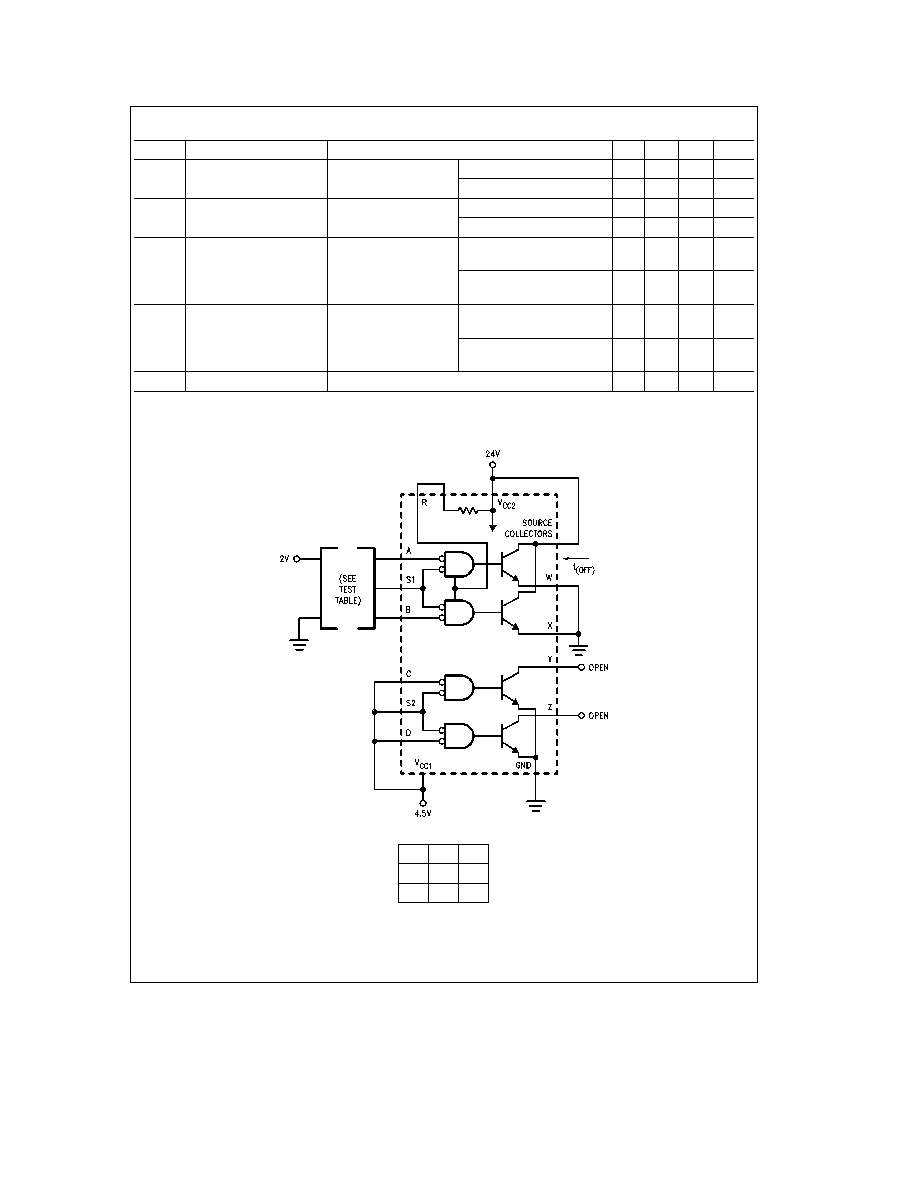
I
OFF
Source Collectors Terminal
V
CC1
e
4 5V V
CC2
e
24V
Full Range
DS55325
500
m
A
``Off'' State Current
(Figure 1)
DS75325
200
m
A
T
A
e
25 C
DS55325
3
150
m
A
DS75325
3
200
m
A
V
OH
High Level Sink Output Voltage
V
CC1
e
4 5V V
CC2
e
24V I
OUT
e
0 mA
(Figure 2)
19
23
V
V
SAT
Saturation Voltage Source
V
CC1
e
4 5V V
CC2
e
15V
Full Range
0 9
V
Outputs
R
L
e
24X
I
SOURCE
b
600 mA
T
A
e
25 C
DS55325
0 43
0 7
V
(Figure 3) (Notes 4 and 6)
DS75325
0 43
0 75
V
V
SAT
Saturation Voltage
V
CC1
e
4 5V V
CC2
e
15V
Full Range
0 9
V
Sink Outputs
R
L
e
24X
I
SINK
600 mA
(Figure 4)
T
A
e
25 C
DS55325
0 43
0 7
V
(Notes 4 and 6)
DS75325
0 43
0 75
V
I
I
Input Current at Maximum
V
CC1
e
5 5V V
CC2
e
24V
Address Inputs
1
mA
Input Voltage
V
I
e
5 5V
(Figure 5)
Strobe Inputs
2
mA
I
IH
High Level Input Current
V
CC1
e
5 5V V
CC2
e
24V
Address Inputs
3
40
m
A
V
I
e
2 4V
(Figure 5)
Strobe Inputs
6
80
m
A
I
IL
Low Level Input Current
V
CC1
e
5 5V V
CC2
e
24V
Address Inputs
b
1
b
1 6
mA
V
I
e
0 4V
(Figure 5)
Strobe Inputs
b
2
b
3 2
mA
I
CC OFF
Supply Current All Sources
V
CC1
e
5 5V V
CC2
e
24V
V
CC1
14
22
mA
and Sinks ``Off''
T
A
e
25 C
(Figure 6)
V
CC2
7 5
20
mA
I
CC1
Supply Current from V
CC1
V
CC1
e
5 5V V
CC2
e
24V I
SINK
e
50 mA
55
70
mA
Either Sink ``On''
T
A
e
25 C
(Figure 7)
I
CC2
Supply Current from V
CC2
V
CC1
e
5 5V V
CC2
e
24V I
SOURCE
e b
50 mA
32
50
mA
Either Source ``On''
T
A
e
25 C
(Figure 8)
Note 1
``Absolute Maximum Ratings'' are those values beyond which the safety of the device cannot be guaranteed Except for ``Operating Temperature Range''
they are not meant to imply that the devices should be operated at these limits The table of ``Electrical Characteristics'' provides conditions for actual device
operation
Note 2
Unless otherwise specified min max limits apply across the
b
55 C to
a
125 C temperature range for the DS55325 and across the 0 C to
a
70 C range for
the DS75325 All typical values are at T
A
e
25 C
Note 3
All currents into device pins shown as positive out of device pins as negative all voltages referenced to ground unless otherwise noted All values shown
as max or min on absolute value basis
Note 4
Only one output at a time should be shorted
Note 5
Voltage values are with respect to network ground terminal
Note 6
These parameters must be measured using pulse techniques t
W
e
200 ms duty cycle
s
2%
2