 | –≠–ª–µ–∫—Ç—Ä–æ–Ω–Ω—ã–π –∫–æ–º–ø–æ–Ω–µ–Ω—Ç: DS75453 | –°–∫–∞—á–∞—Ç—å:  PDF PDF  ZIP ZIP |
DS75451/2/3
Series Dual Peripheral Drivers
General Description
The DS7545X series of dual peripheral drivers is a family of
versatile devices designed for use in systems that use TTL
logic. Typical applications include high speed logic buffers,
power drivers, relay drivers, lamp drivers, MOS drivers, bus
drivers and memory drivers.
The DS75451, DS75452 and DS75453 are dual peripheral
AND, NAND and NOR drivers, respectively, (positive logic)
with the output of the logic gates internally connected to the
bases of the NPN output transistors.
Features
n
300 mA output current capability
n
High voltage outputs
n
No output latch-up at 20V
n
High speed switching
n
Choice of logic function
n
TTL compatible diode-clamped inputs
n
Standard supply voltages
n
Replaces TI "A" and "B" series
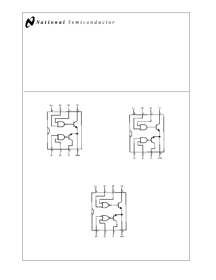
Connection Diagrams
(Dual-In-Line and Metal Can Packages)
DS005824-2
*
See (Note 5) and Appendix E regarding S.O. package power dissipation
constraints.
Top View
Order Number DS75451M or DS75451N
DS005824-3
Top View
Order Number DS75452M or DS75452N
See NS Package Numbers M08A
*
or N08E
DS005824-4
*
See (Note 5) and Appendix E regarding S.O. package power dissipation constraints.
Top View
Order Number DS75453M or DS75453N
See NS Package Numbers M08A
*
or N08E
February 2000
DS75451/2/3
Series
Dual
Peripheral
Drivers
© 2000 National Semiconductor Corporation
DS005824
www.national.com
Absolute Maximum Ratings
(Note 1)
If Military/Aerospace specified devices are required,
please contact the National Semiconductor Sales Office/
Distributors for availability and specifications.
Supply Voltage, (V
CC
) (Note 2)
7.0V
Input Voltage
5.5V
Inter-Emitter Voltage (Note 3)
5.5V
Output Voltage (Note 4)
30V
Output Current (Note 5)
300 mA
Maximum Power (Note 5)
Dissipation
at 25∞C
Molded DIP Package
957 mW
SO Package
632 mW
Storage Temperature Range
-65∞C to +150∞C
Lead Temperature (Soldering, 4 sec.)
260∞C
Operating Conditions
Min
Max
Units
Supply Voltage, (V
CC
)
4.75
5.25
V
Temperature, (T
A
)
0
+70
∞C
Derate molded package 7.7 mW/∞C above 25∞C, derate SO package 7.56
mW/∞C above 25∞C.
Electrical Characteristics
(Notes 6, 7)
Symbol
Parameter
Conditions
Min
Typ Max Units
V
IH
High-Level Input Voltage
(
Figure 7)
2
V
V
IL
Low-Level Input Voltage
0.8
V
V
I
Input Clamp Voltage
V
CC
= Min, I
I
= -12 mA
-1.5
V
V
OL
Low-Level Output Voltage
V
CC
=
Min,
(
Figure 7)
V
IL
= 0.8V
I
OL
= 100 mA
DS75451, DS75453
0.25
0.4
V
I
OL
= 300 mA
DS75451, DS75453
0.5
0.7
V
V
IH
= 2V
I
OL
= 100 mA
DS75452
0.25
0.4
V
I
OL
= 300 mA
DS75452
0.5
0.7
V
I
OH
High-Level Output Current
V
CC
=
Min,
(
Figure 7)
V
OH
= 30V
V
IH
= 2V
DS75451, DS75453
100
µA
V
IL
= 0.8V
DS75452
100
µA
I
I
Input Current at Maximum
Input Voltage
V
CC
= Max, V
I
= 5.5V, (Figure 9)
1
mA
I
IH
High-Level Input Current
V
CC
= Max, V
I
= 2.4V, (Figure 9 )
40
µA
I
IL
Low-Level Input Current
V
CC
= Max, V
I
= 0.4V, (Figure 8)
-1
-1.6
mA
I
CCH
Supply Current, Outputs
High
V
CC
=
Max,
(
Figure
10)
V
I
= 5V
DS75451
7
11
mA
V
I
= 0V
DS75452
11
14
mA
V
I
= 5V
DS75453
8
11
mA
I
CCL
Supply Current, Outputs
Low
V
CC
=
Max,
(
Figure
10)
V
I
= 0V
DS75451
52
65
mA
V
I
= 5V
DS75452
56
71
mA
V
I
= 0V
DS75453
54
68
mA
Switching Characteristics
(V
CC
= 5V, T
A
= 25∞C)
Symbol
Parameter
Conditions
Min
Typ Max
Units
t
PLH
Propagation Delay Time, Low-to-High
Level Output
C
L
= 15 pF, R
L
= 50
,
I
O
200 mA, (
Figure 14)
DS75451
18
25
ns
DS75452
26
35
ns
DS75453
18
25
ns
t
PHL
Propagation Delay Time, High-to-Low
Level Output
C
L
= 15 pF, R
L
= 50
,
I
O
200 mA, (
Figure 14)
DS75451
18
25
ns
DS75452
24
35
ns
DS75453
16
25
ns
t
TLH
Transition Time, Low-to-High Level
Output
C
L
= 15 pF, R
L
= 50
, I
O
200 mA,
(
Figure 14)
5
8
ns
t
THL
Transition Time, High-to-Low Level
Output
C
L
= 15 pF, R
L
= 50
, I
O
200 mA,
(Figure 14 )
7
12
ns
DS75451/2/3
www.national.com
2
Switching Characteristics
(Continued)
Symbol
Parameter
Conditions
Min
Typ Max
Units
V
OH
High-Level Output Voltage after
Switching
V
S
= 20V, I
O
300 mA, (
Figure 15)
V
S
- 6.5
mV
Note 1: "Absolute Maximum Ratings" are those values beyond which the safety of the device cannot be guaranteed. Except for "Operating Temperature Range" they
are not meant to imply that the devices should be operated at these limits. The table of "Electrical Characteristics" provides conditions for actual device operation.
Note 2: Voltage values are with respect to network ground terminal unless otherwise specified.
Note 3: The voltage between two emitters of a multiple-emitter transistor.
Note 4: The maximum voltage which should be applied to any output when it is in the "OFF" state.
Note 5: Both halves of these dual circuits may conduct rated current simultaneously; however, power dissipation averaged over a short time interval must fall within
the continuous dissipation rating.
Note 6: Unless otherwise specified min/max limits apply across 0∞C to +70∞C range. All typicals are given for V
CC
= +5V and T
A
= 25∞C.
Note 7: All currents into device pins shown as positive, out of device pins as negative, all voltages referenced to ground unless otherwise noted. All values shown
as max or min on absolute value basis.
Truth Tables
(H = high level, L = low level)
DS75451
A
B
Y
L
L
L (ON State)
L
H
L (ON State)
H
L
L (ON State)
H
H
H (OFF State)
DS75452
A
B
Y
L
L
H (OFF State)
L
H
H (OFF State)
H
L
H (OFF State)
H
H
L (ON State)
DS75453
A
B
Y
L
L
L (ON State)
L
H
H (OFF State)
H
L
H (OFF State)
H
H
H (OFF State)
DS75451/2/3
www.national.com
3

Schematic Diagrams
DS75451
DS005824-11
Resistor values shown are nominal.
DS75452
DS005824-12
Resistor values shown are nominal.
DS75453
DS005824-13
Resistor values shown are nominal.
DS75451/2/3
www.national.com
4

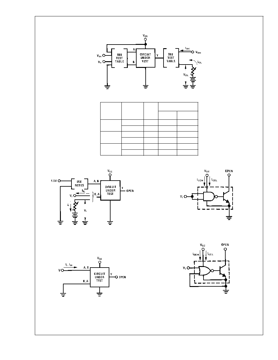
DC Test Circuits
DS005824-15
Both inputs is tested simultaneously.
FIGURE 1. V
IH
, V
OL
DS005824-16
Each input is tested separately.
FIGURE 2. V
IL
, V
OH
DS005824-17
Each input is tested separately.
FIGURE 3. V
I
, I
IL
DS005824-18
Each input is tested separately.
FIGURE 4. I
I
, I
IH
DS005824-19
Each input is tested separately.
FIGURE 5. I
OS
DS005824-20
Both gates are tested simultaneously.
FIGURE 6. I
CCH
, I
CCL
DS75451/2/3
www.national.com
5
DC Test Circuits
(Continued)
DS005824-21
Circuit
Input
Under
Test
Other
Input
Output
Apply
Measure
DS75451
V
IH
V
IH
V
OH
I
OL
V
IL
V
CC
I
OL
V
OL
DS75452
V
IH
V
IH
I
OL
V
OL
V
IL
V
CC
V
OH
I
OH
DS75453
V
IH
Gnd
V
OH
I
OH
V
IL
V
IL
I
OL
V
OH
FIGURE 7. V
IH
, V
IL
, I
OH
, V
OL
DS005824-22
Note A: Each input is tested separately.
Note B: When testing DS75453 input not under test is grounded.
For all other circuits it is at 4.5V.
FIGURE 8. V
I
, V
IL
DS005824-23
Each input is tested separately.
FIGURE 9. I
I
, I
IH
DS005824-24
Both gates are tested simultaneously.
FIGURE 10. I
CCH
, I
CCL
for AND, NAND Circuits
DS005824-25
Both gates are tested simultaneously.
FIGURE 11. I
CCH
, I
CCL
for OR, NOR Circuits
DS75451/2/3
www.national.com
6
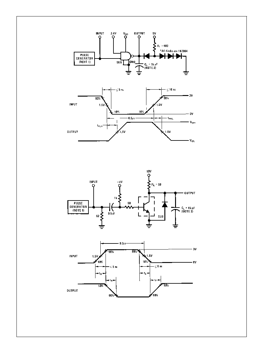
AC Test Circuits and Switching Time Waveforms
DS005824-26
DS005824-27
Note 1: The pulse generator has the following characteristics: PRR = 1 MHz, Z
OUT
50
.
Note 2: C
L
includes probe and jig capacitance.
FIGURE 12. Propagation Delay Times, Each Gate
DS005824-28
DS005824-29
Note 1: The pulse generator has the following characteristics: duty cycle
1%, Z
OUT
50
.
Note 2: C
L
includes probe and jig capacitance.
FIGURE 13. Switching Times, Each Transistor
DS75451/2/3
www.national.com
7
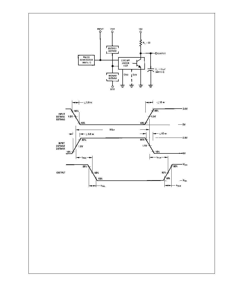
AC Test Circuits and Switching Time Waveforms
(Continued)
DS005824-30
DS005824-31
Note 1: The The pulse generator has the following characteristics: PRR = 1.0 MHz, Z
OUT
50
.
Note 2: C
L
includes probe and jig capacitance.
FIGURE 14. Switching Times of Complete Drivers
DS75451/2/3
www.national.com
8
AC Test Circuits and Switching Time Waveforms
(Continued)
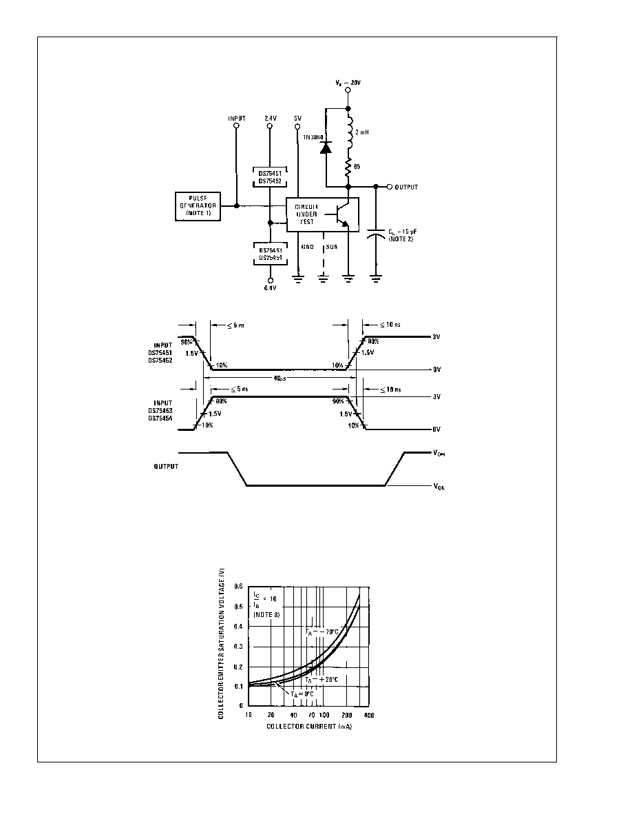
Typical Performance Characteristics
DS005824-32
DS005824-33
Note 1: The pulse generator has the following characteristics: PRR = 12.5 kHz, Z
OUT
50
.
Note 2: C
L
includes probe and jig capacitance.
FIGURE 15. Latch-UP Test of Complete Drivers
DS005824-37
FIGURE 16. Transistor Collector-Emitter Saturation Voltage vs Collector Current
DS75451/2/3
www.national.com
9

Typical Applications
DS005824-46
*
Optional keep-alive resistors maintain off-state lamp current at
10% to reduce surge current.
FIGURE 17. Dual Lamp or Relay Driver
DS005824-47
FIGURE 18. Complementary Driver
DS005824-48
FIGURE 19. TTL or DTL Positive Logic-Level Detector
DS75451/2/3
www.national.com
10

Typical Applications
(Continued)
DS005824-49
*
The two input resistors must be adjusted for the level of MOS input.
FIGURE 20. MOS Negative Logic-Level Detector
DS75451/2/3
www.national.com
11

Typical Applications
(Continued)
DS005824-50
FIGURE 21. Logic Signal Comparator
DS005824-51
*
If inputs are unused, they should be connected to +5V through a 1k resistor.
DS005824-52
Low output occurs only when inputs are low simultaneously.
FIGURE 22. In-Phase Detector
DS75451/2/3
www.national.com
12

Physical Dimensions
inches (millimeters) unless otherwise noted
SO Package (M)
Order Number DS75451M, DS75452M, DS75453M
NS Package Number M08A
Molded Dual-In-Line Package (N)
Order Number DS75451N, DS75452N, DS75453N
NS Package Number N08E
DS75451/2/3
www.national.com
13
Notes
LIFE SUPPORT POLICY
NATIONAL'S PRODUCTS ARE NOT AUTHORIZED FOR USE AS CRITICAL COMPONENTS IN LIFE SUPPORT
DEVICES OR SYSTEMS WITHOUT THE EXPRESS WRITTEN APPROVAL OF THE PRESIDENT AND GENERAL
COUNSEL OF NATIONAL SEMICONDUCTOR CORPORATION. As used herein:
1. Life support devices or systems are devices or
systems which, (a) are intended for surgical implant
into the body, or (b) support or sustain life, and
whose failure to perform when properly used in
accordance with instructions for use provided in the
labeling, can be reasonably expected to result in a
significant injury to the user.
2. A critical component is any component of a life
support device or system whose failure to perform
can be reasonably expected to cause the failure of
the life support device or system, or to affect its
safety or effectiveness.
National Semiconductor
Corporation
Americas
Tel: 1-800-272-9959
Fax: 1-800-737-7018
Email: support@nsc.com
National Semiconductor
Europe
Fax: +49 (0) 180-530 85 86
Email: europe.support@nsc.com
Deutsch Tel: +49 (0) 69 9508 6208
English
Tel: +44 (0) 870 24 0 2171
FranÁais Tel: +33 (0) 1 41 91 8790
National Semiconductor
Asia Pacific Customer
Response Group
Tel: 65-2544466
Fax: 65-2504466
Email: ap.support@nsc.com
National Semiconductor
Japan Ltd.
Tel: 81-3-5639-7560
Fax: 81-3-5639-7507
www.national.com
DS75451/2/3
Series
Dual
Peripheral
Drivers
National does not assume any responsibility for use of any circuitry described, no circuit patent licenses are implied and National reserves the right at any time without notice to change said circuitry and specifications.