TL F 5796
DS7820DS8820
Dual
Line
Receiver
February 1996
DS7820 DS8820 Dual Line Receiver
General Description
The DS7820 specified from
b
55 C to
a
125 C and the
DS8820 specified from 0 C to
a
70 C are digital line re-
ceivers with two completely independent units fabricated on
a single silicon chip Intended for use with digital systems
connected by twisted pair lines they have a differential in-
put designed to reject large common mode signals while
responding to small differential signals The output is direct-
ly compatible with TTL or LS integrated circuits
The response time can be controlled with an external ca-
pacitor to eliminate noise spikes and the output state is
determined for open inputs Termination resistors for the
twisted pair line are also included in the circuit Both the
DS7820 and the DS8820 are specified worst case over
their full operating temperature range for
g
10-percent sup-
ply voltage variations and over the entire input voltage
range
Features
Y
Operation from a single
a
5V logic supply
Y
Input voltage range of
g
15V
Y
Each channel can be strobed independently
Y
High input resistance
Y
Fan out of two with TTL integrated circuits
Y
Strobe low forces output to ``1'' state
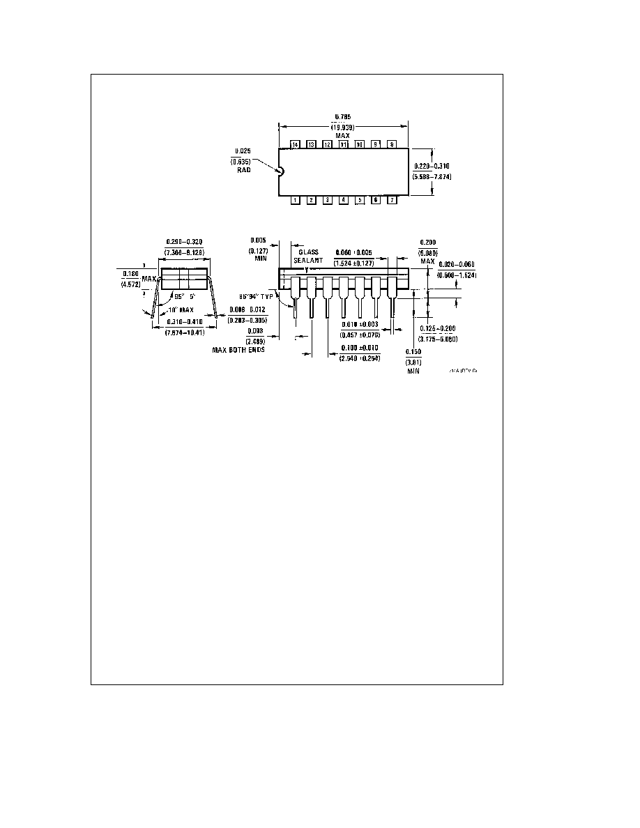
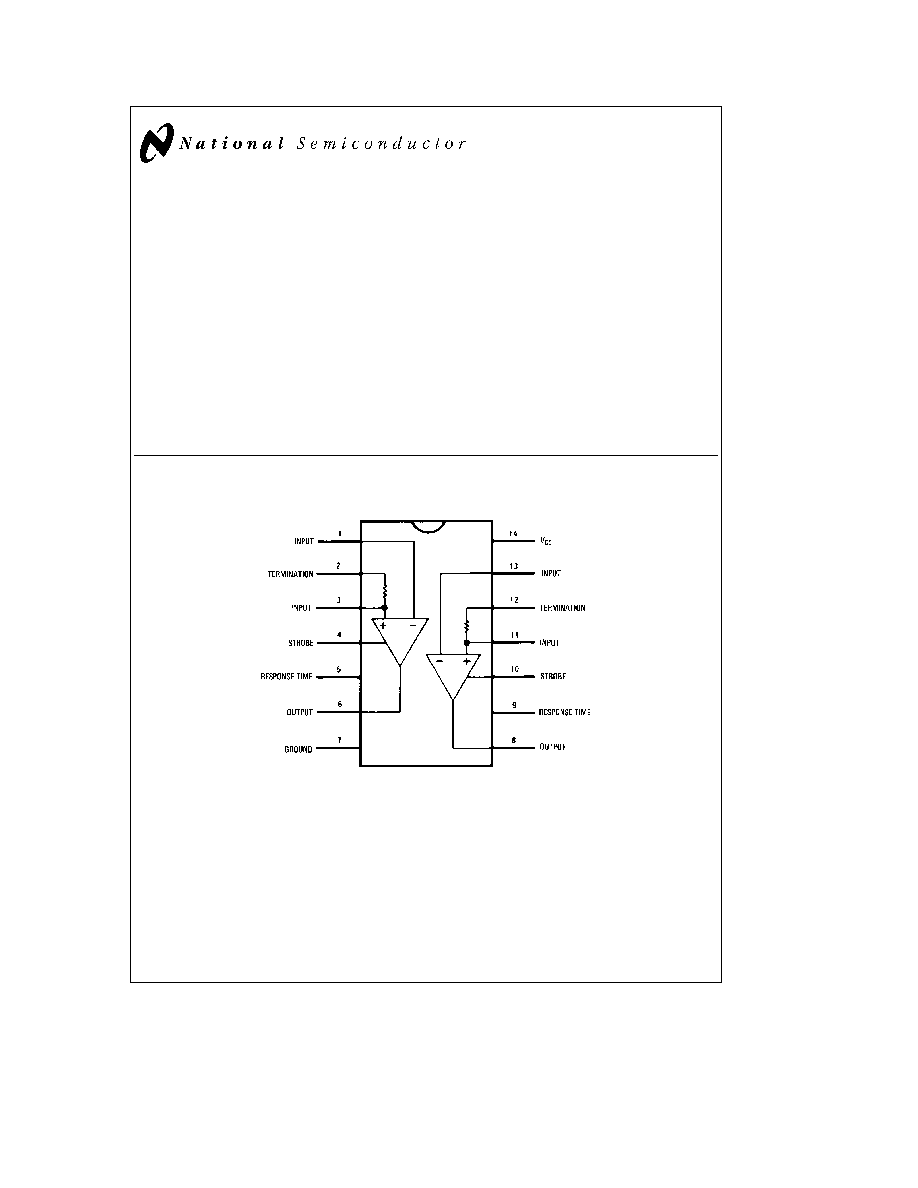
Connection Diagram
Dual-In-Line Package
TL F 5796 ≠ 2
Top View
Order Number DS7820J or DS8820N
See NS Package Number J14A or N14A
For Complete Military 883 Specifications See RETS Data Sheet
Order Number DS7820J 883 or DS7820W 883
See NS Package Number J14A or W14B
C1996 National Semiconductor Corporation
RRD-B30M36 Printed in U S A
http
www national com
Absolute Maximum Ratings
(Note 1)
If Military Aerospace specified devices are required
please contact the National Semiconductor Sales
Office Distributors for availability and specifications
Supply Voltage
8 0V
Input Voltage
g
20V
Differential Input Voltage
g
20V
Strobe Voltage
8 0V
Output Sink Current
25 mA
Storage Temperature Range
b
65 C to
a
150 C
Lead Temperature (Soldering 4 sec )
260 C
Maximum Power Dissipation at 25 C
Cavity Package
1308 mW
Molded Package
1207 mW
Derate cavity package 8 7 mW C above 25 C derate molded package
9 7 mW C above 25 C
Operating Conditions
Min
Max
Units
Supply Voltage (V
CC
)
DS7820
4 5
5 5
V
DS8820
4 75
5 25
V
Temperature (T
A
)
DS7820
b
55
a
125
C
DS8820
0
a
70
C
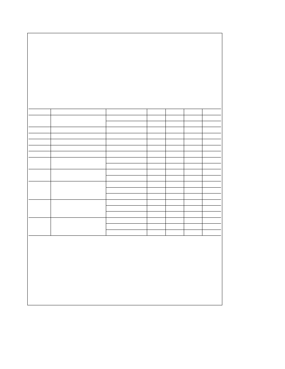
Electrical Characteristics
(Notes 2 and 3)
Symbol
Parameter
Conditions
Min
Typ
Max
Units
V
TH
Input Threshold Voltage
V
CM
e
0V
b
0 5
0
0 5
V
b
15V
s
V
CM
s
15V
b
1 0
0
1 0
V
V
OH
High Output Level
I
OUT
s
0 2 mA
2 5
5 5
V
V
OL
Low Output Level
I
SINK
s
3 5 mA
0
0 4
V
R
I
b
Inverting Input Resistance
3 6
5 0
kX
R
I
a
Non-Inverting Input Resistance
1 8
2 5
kX
R
T
Line Termination Resistance
T
A
e
25 C
120
170
250
X
t
r
Response Time
C
DELAY
e
0 pF
40
ns
C
DELAY
e
100 pF
150
ns
I
ST
Strobe Current
V
STROBE
e
0 4V
b
1 0
b
1 4
mA
V
STROBE
e
5 5V
5 0
m
A
I
CC
Power Supply Current
V
IN
e
15V
3 2
6 0
mA
V
IN
e
0V
5 8
10 2
mA
V
IN
e b
15V
8 3
15 0
mA
I
IN
a
Non-Inverting Input Current
V
IN
e
15V
5 0
7 0
mA
V
IN
e
0V
b
1 6
b
1 0
mA
V
IN
e b
15V
b
9 8
b
7 0
mA
I
IN
b
Inverting Input Current
V
IN
e
15V
3 0
4 2
mA
V
IN
e
0V
0
b
0 5
mA
V
IN
e b
15V
b
4 2
b
3 0
mA
Note 1
``Absolute Maximum Ratings'' are those values beyond which the safety of the device cannot be guaranteed Except for ``Operating Temperature Range''
they are not meant to imply that the devices should be operated at these limits The table of ``Electrical Characteristics'' provides conditions for actual device
operation
Note 2
These specifications apply for 4 5V
s
V
CC
s
5 5V
b
15V
s
V
CM
s
15V and
b
55 C
s
T
A
s
a
125 C for the DS7820 or 0 C
s
T
A
s
a
70 C for the
DS8820 unless otherwise specified typical values given are for V
CC
e
5 0V T
A
e
25 C and V
CM
e
0 unless stated differently
Note 3
All currents into device pins shown as positive out of device pins as negative all voltages referenced to ground unless otherwise noted All values shown
as max or min on absolute value basis
Note 4
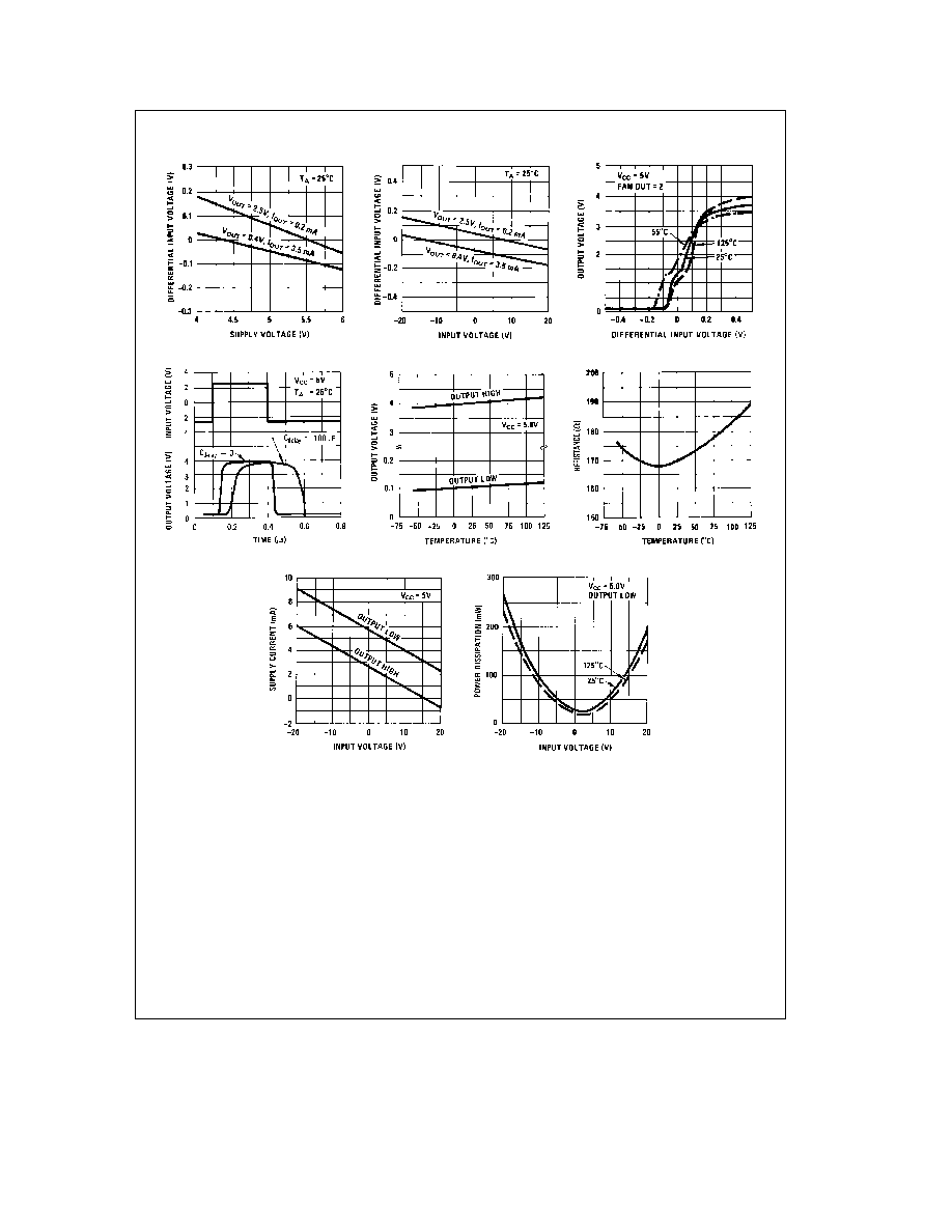
The specifications and curves given are for one side only Therefore the total package dissipation and supply currents will be double the values given when
both receivers are operated under identical conditions
http
www national com
2